Note: Descriptions are shown in the official language in which they were submitted.
CA 0222601~ 1997-12-30
W O 97/0260S PCT/CA35~_~
METHOD OF FABRICATING A FAST PROGRAMMING FLASH E2PROM CELL
F;el~ of ~he Tnvent;on
The present invention relates in general to
Electrically Erasable and Programmable Read-Only Memory
(E2PROM), and more particularly to a method of fabricating
a flash E2PROM with fast programming speed and low
operating voltages.
Rackgrotlnd of the Tnvent;on
Flash memory is a modified form of E2PROM which can
be erased one block at a time and can be programmed one
bit at a time. At the time of filing this application,
flash memory chips are available in densities of up to
32M bits. Large data storage capacity with complete
nonvolatility, results in numerous applications for such
chips, ranging from cellular telephones, solid-state
disks and memory cards. Such applications have
traditionally been the domain of ROM, conventional E2PROM,
battery-backed RAM, static RAM (SRAM) and magnetic
storage.
A flash E2PROM cell resembles an ordinary MOS (Metal-
Oxide-Semiconductor) transistor, except for the addition
of a floating gate, which is buried in the insulator
between the substrate and the conventional control gate.
Charge stored on the floating gate alters the threshold
voltage (Vth) of the device as measured at the control
gate. Since the floating gate and the control gate are
both stacked directly above the transistor channel, very
high densities can be achieved. Even higher densities
can be obtained by self aligning the control and floating
a 35 gates to the source and drain regions.
The cell is programmed and erased by adding
electrons to and removing electrons from the floating
gate, respectively. A cell with a high threshold voltage
CA 022260l~ l997-l2-30
W O 97/0260S PCT/CA~5/~_11C
(Vth) is in its "0" state. After erasure has been
completed, the threshold voltage is reduced resulting in
a "1" state. The con~llctivity of the ~h~nn~l determines
the information stored in the memory cell (i.e. current
flowing through the ch~nn~l is detected by sense-
amplifier circuitry as a "1", while the absence of
current is detected as a "0").
Flash E2PROM technology has received industry-wide
attention recently. Due to its simple single transistor
cell architecture, flash memory may eventually cost less
to make than DRAM (Dynamic Random Access Memory).
The channel hot electron programming method, used in
conventional flash E2PROM cells, requires biasing the
device at high drain voltage (6 to 8V) to generate hot
electrons. This results in additional circuit complexity
and cost (ie. an additional external voltage supply),
which is a particular disadvantage in mobile applications
such as cellular telephones, etc.
Furthermore, the channel hot electron injection
method used for programming conventional flash E2PROM
cells, generates very high lateral source-to-drain
currents (in the range of milliamperes). These high
currents limit the number of cells that can be programmed
at one time.
Existing flash E2PROM cells also suffer from slow
programming speed (~lO~s) which prevents their widespread
application as a replacement for RAMs and electronic hard
disks. If the device gate length is scaled down in order
to reduce the programming time, then punchthrough between
the source and drain is likely to occur. 6
D;scll~s;on of Pr;or ~rt
CA 022260l~ l997-l2-30
W O 97/02605 PCT/CA9~ 11C
A well known early prior art pr~Pc~csor to modern
day flash memory devices is the FAMOS (floating-gate
avalanche-injection MOS) memory. This device is
described in a number of publications, including: Dov
Frohman-Bentchowsky, "A Fully Decoded 2048-Bit
Electrically Programmable FAMOS Read-Only Memory"; IEEE
Journal of Solid State Circuits, Vol. SC-6, No. 5,
October 1971, pp 301-306; Ron D. Katznelson and Dov
Frohman-Bentchowsky, "An Erase Model for FAMOS EPROM
Devices"; IEEE Transactions on Electron Devices, Vol. ED-
27, No. 9, September 1980, pp 1744-1752; and U.S. Patent
No. 4,203,158 (Frohman-Bentchkowsky, et al).
Another prior art flash memory device is described
in Masatada Horiuchi and Hisao Katto,"FCAT-A Low-Voltage
High Speed Alternative n-Channel Nonvolatile Memory
Device"; Transactions on Electron Devices, Vol. ED-26,
No. 6, June 1979, pp. 914-918. The FCAT cell has the p+
regions placed outside the channel area corners adjacent
to the diffused n+ source and/or drain regions. This
method of positioning the p+ regions results in a corner
point injection for the hot electrons which contributes
to acute stress in the tunnel oxide. Also, the FCAT cell
uses hot hole injection into the thin gate oxide for
erasure, which can lead to poor reliability and endurance
characteristics.
U.S. Patent 5,464,785 entitled "Method of M~k;ng A
Flash EPROM Device Having A Drain Edge P+ Implant", (Hong
et al.), describes a flash EPROM structure with a drain
edge p+ implant that utilizes the electric field at the
junction between the drain and implant to enhance the
generation and injection of hot channel electrons during
programming operation. According to Hong et al., the
drain edge p+ implant extends across the entire width of
the EPROM cell, thereby preventing lateral current flow
through the MOS channel between the source and drain.
CA 022260l~ l997-l2-30
W O 97/02605 PCT/CA~6.'~C1~6
Therefore, the data stored in the cell cannot be sensed
readily.
The fabrication steps suggested by Hong et. al. are
impractical since it is very difficult to etch the narrow
vertical trenches (reported typically to be 1000A wide by
5000~ high) used for the drain edge p+ implant. Also, the
fabrication steps imply a dedicated process which is not
CMOS compatible.
No read, write, and erase schemes are described in
the Hong et al. patent, nor is any evidence of
experimental performance indicated.
S~mm~ry of the Tnvention
According to the present invention, a low voltage
flash E2PROM cell is provided which overcomes the above-
identified programming speed limitations of conventional
prior art flash memory cells, and in addition allows the
cell to operate at low voltages.
More particularly, the flash EZPROM cell is
comprised of two sections which are butted together. One
portion (width-wise) is covered by a highly doped p+
pocket implant adjacent to at least one of the n+ source
and drain regions. This portion is referred to as the
program section. The remaining portion (width-wise) is
not covered by the highly doped p+ pocket implant and
resembles a conventional EZPROM cell. This portion is
referred to as the sense section.
The highly doped p+ pocket implant and the n+ drain
and/or source regions create a junction having narrow
depletion width such that when the junction is reverse
biased an electric field is created for generating hot
electrons for storage on the floating gate, thereby
CA 0222601~ 1997-12-30
W O 97/02605 PCT/CAg5~0
programming the flash E2PROM. The programming speed of the
im~o~ed flash E2PROM cell of the present invention is in
general an order of magnitude faster than a conventional
flash E2PROM cell of the same dimension. The doping
5 ço~c~ntration of the p+ pocket implant is chosen such that
the junction will breakdown at low voltages (typically in
the range of 2.5 to 5V), thus enabling the drain and/or
source regions to be driven directly by the logic level
supply voltages. This eliminates the need for large
charge pump circuits with high current capacity as used
in conventional flash E2PROMs. The enhancement of hot
electron generation results in smaller drain and/or
source currents (typically in the range of 50 to 200~A/~m
of cell width) than prior art devices during the
programming operation. Thus, the flash E2PROM cell of the
present invention consumes much less power, and is more
suitable for battery operated portable equipment than
similar prior art devices.
High positive and negative voltages are needed only
to drive the control gate. Consequently, they can be
generated on-chip using simple charge pump circuitry with
small current driving capability. The voltages required
at the source and drain in all modes of operation can be
obtained directly from a low power supply rail.
The flash E2PROM cell of the present invention is
compatible with CMOS and BiCMos processes. More
particularly, according to one aspect of the present
invention, a method of fabricating an E2PROM cell is
provided in which the fabrication steps are modular and
compatible with conventional CMOS and BiCMoS process
flows. Cell fabrication can be integrated into existing
- CMOS and BiCMOS processes with minimal changes. The
resulting flash E2PROM cell is a self aligned structure.
The p+ pocket implant is carried out in the same way as
the n-LDD implant commonly used in modern CMOS and BiCMoS
CA 0222601~ 1997-12-30
W O 97/02605 PCT/CAg'~ C
processes. The generation of hot electrons is dependent
on the doping level of the p+/n+ junction rather than the
size of the channel length. The electric field at this
junction ( ~ 106 V/cm) significantly exceeds the maximum
lateral electric field ( ~ 105 V/cm) available in
conventional flash E2PROM cells with short channel lengths
(0.3 to 0.5~m), thus ensuring very efficient injection of
hot electrons into the floating gate.
Rr;ef Tntro~uction to the Dr~wings
Detailed descriptions of one prior art flash memory
cell and of flash E2PROM cells according to a first
embodiment and a preferred embodiment of the present
invention are provided herein below, with reference to
the following drawings, in which:
Figure 1 is a schematic representation of a prior
art flash E2PROM cell;
Figure 2 is a schematic representation of hot
electron injection programming of the prior art flash
memory cell depicted in Figure 1;
Figure 3 is a schematic representation of erasure of
the prior art flash memory cell depicted in Figure 1
using Fowler-Nordheim tunnelling across the thin gate
oxide;
Figure 4 is a schematic representation of the read
operation of the prior art flash memory cell depicted in
Figure l;
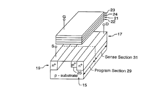
Figure 5 is a three-dimensional schematic
representation of a flash E2PROM cell according to a first
embodiment of the present invention;
CA 0222601~ 1997-12-30
W O 97/02605 PCT/CA~C~ 1S~
Figure 6 is a three-dimensional schematic
representation of Zener and/or avalanche breakdown-based
electron injection programming of the flash E2PROM cell of
Figure 5;
Figure 7 is a three-dimensional schematic
representation of the read operation of the flash E2PROM
cell of Figure 5;
Figure 8 is a three-dimensional schematic
representation of the erasure operation of the flash
E2PROM cell of Figure 5;
Figure 9 is a three~ n~cional schematic
representation of the preferred embodiment of flash E2PROM
cell according to the present invention;
Figure 10 is a plan view of the device shown in
Figure 9;
Figures ll(a) through ll(r) depict the process flow
steps for fabricating the flash E2PROM cell according to
the present invention;
Figures 12A and 12B show a circuit diagram and
cross-sectional diagram, respectively, of the flash E2PROM
cell of the preferred embodiment configured in a cross
point array architecture;
Figure 13 shows a simulation of programming time as
a function of channel length for different p+ doping
~ concentrations for the preferred embodiment of Figure 9;
- Figure 14 shows simulated and measured programming
characteristics for the preferred embodiment of Figure g;
and
CA 0222601~ 1997-12-30
W O 97/0260S PCT/CA951~-~C
Figure 15 shows the experimental effect of the p+/n+
junction on the disturb characteristics of a half-
selected programmed and erased E2PROM cell according to
the preferred embodiment of Figure 9.
Detailed Description of the Prior Art ETOX~ Memory Cell
Turning to Figure 1, a flash E2PROM cell is shown
(ETOX~ cell by Intel Corp.), having a floating gate 1 and
a control gate 3 stacked vertically above the MOFSET
channel 5 in substrate 6 intermediate the source 7 and
drain 9. A tunnel oxide 11 is provided intermediate the
floating gate 1 and channel 5, and an inter-poly oxide 13
is provided intermediate the floating gate 1 and control
gate 3.
In order to program the ETOX~ flash memory cell of
Figure 1, a voltage of +12V is applied to the control
gate 3, the source 7 is grounded, and approximately +6V
is applied between source 7 and drain 9 as shown in
Figure 2. As discussed above, the control gate 3 is
capacitively coupled to the floating gate 1.
The source-drain voltage (+6V) generates hot
electrons that are swept across the channel 5 from source
7 to drain 9. These hot electrons collide with atoms in
the channel 5 thereby creating additional hot electrons.
The high voltage (+12V) on control gate 3 attracts the
hot electrons across the thin tunnel oxide 11 where they
accumulate on the floating gate 1. When enough electrons
have accumulated, the cell switches from its "1" (erased)
state to its "0" (programmed) state.
As the floating gate 1 becomes fully charged, the
current across the oxide 11 reduces almost to zero as a
result of the electric field in the oxide 11 becoming
CA 0222601~ 1997-12-30
W O 97/02605 PCT/CAg6/00446
repulsive to additional electron injection from the high
electric field region at the drain 9. Therefore,
electron injection during programming is a self limiting
process.
s
The voltage applied to the drain 9 does not, in
general, have a significant effect on the programmed
threshold voltage of the EEPROM cell. However, it does
affect the speed of programming of the device.
To erase a flash memory cell, Fowler-Nordheim
tunnelling is used to remove electrons from the floating
gate 1. More particularly, by floating the drain 9,
grounding the control gate 3 and applying +12V to the
source 7, an electric field is generated across the thin
tunnel oxide 11 between the floating gate 1 and the
source 7. This electric field attracts electrons off of
the floating gate 1 toward the source 7, as shown in
Figure 3.
When all of the excess electrons have been removed
from the floating gate 1, the threshold voltage (Vth)
returns to its initial value thereby resetting the cell
to a "l" state.
During reading, the prior art ETOX~ memory cell
operates like an ordinary transistor. When the flash
memory is read, address inputs select specific
transistors within the memory cell array. Supply-voltage
levels are applied to the control gate 3 and drain 9,
while the source 7 is grounded as shown in Figure 4. By
sensing the amount of current that is conducted in the
channel 5 between the source 7 and the drain 9, it is
- possible to determine if the cell has been programmed or
erased, as discussed above.
Det~ Descr;~t;on of ~
CA 0222601~ 1997-12-30
W O 97/02605 PCT/CA~5~'~~2~C
First Embodiment of Flash E2PROM Cell
Turning now to Figure S, a flash E2PROM cell is shown
for achieving simultaneous reduction of programming time
and operating voltages over the prior art cell of Figure
1.
The cell according to the present invention
comprises a substrate 15, drain and source regions 17 and
19, respectively, a floating gate 21 and control gate 23,
in the usual manner. Tunnel and inter-poly dielectric
layers 22 and 24 are also provided in the usual manner.
However, in contrast with the prior art ETOX~ flash
memory cell, additional highly doped regions 25 and 27
lS are provided adjoining the drain and/or source regions 17
and/or 19, respectively. The additional highly doped
regions 25 and 27 (occasionally referred to herein as
pocket implants) extend along a portion of the width of
the cell structure identified as the program section 29,
the remaining sense section 31 being provided for the
read operation of the cell, as discussed in greater
detail below.
In the illustrated embodiment, the substrate is made
of p-type material, the drain and source regions are
fabricated from n+-type material, and the additional
highly doped regions 25 and 27 comprise p+-type regions.
According to the present invention, programming is
accomplished via low voltage Zener and/or avalanche
breakdown at the reverse biased p+/n+ junctions in the
program section 29. High doping concentrations at these
junctions results in a narrow depletion width so that
only a small voltage is required to generate a
sufficiently strong electric field to create hot
electrons for storage on the floating gate 21.
CA 022260l~ l997-l2-30
W O 97/02605 PCT/CA95/~116
11
The breakdown mechAn;sm which dominates and the
applied voltage required for breakdown depend on the
doping of the p+ regions. Computer simulation results
have shown that p+ doping concentrations in the range of
lxl0l8cm~3 to 5xl0l9cm~3 are suitable for the implementation
of this structure.
As indicated above, the cell is programmed and read
from the program and sense sections 29 and 31,
respectively, and erased by Fowler-Nordheim tunnelling of
electrons from the floating gate 21 to the source 19.
With reference to Figure 6, a schematic
representation of the programming mode of operation is
provided. In order to program a logic "0" into the cell,
sufficient electrons must be stored on the floating gate
21 to raise the transistor threshold voltage (Vth) so that
the normal read voltage (e.g. 5 Volts) applied to control
gate 23 is insufficient to turn the transistor on.
Accordingly, low positive voltages (less than SV)
are applied to the drain 17 and source 19 while a high
programming voltage (in the range of 10 to 15 Volts) is
applied to control gate 23. The substrate 15 is
grounded. Low voltage Zener and/or avalanche breakdown
at the reversed biased p+/n+ junctions, results in the
generation of hot electrons which are drawn to the
floating gate 21 as a result of the high voltage applied
to control gate 23.
In contrast with the prior art ETOX~ memory cell,
~ the generation of hot electrons necessary to program the
flash memory cell of the present invention does not
- require a large drain-to-source current flow. This is a
result of the high electric field (e.g. 106V/cm) generated
in the narrow depletion regions 26 associated with the
heavily doped p+/n+ junctions.
CA 022260l~ l997-l2-30
W 0 97/02605 PCT/CA96/00446 12
Figure 7 schematically shows the read mode operation
of the flash memory cell according to the present
invention. In operation, a low read voltage (e.g. +5
Volts) is applied to control gate 23; a voltage lower
than the breakdown voltage of the p+/n+ junction is
applied to the drain 17 (e.g. 13 volts), and the source
19 and substrate 15 are grounded. Operation in the read
mode is essentially the same as discussed above with
respect to the ETOX~ prior art memory cell. In
particular, in an erased cell, the voltage applied to
control gate 23 is sufficient to overcome the transistor
turn-on threshold voltage (Vth), and the drain-to-source
current is detected in the sense section 31 by sense
amplifier circuitry (not shown) and translated into a
logic "1". Conversely, in a programmed cell, the added
electrons stored on the floating gate 21 raise the
transistor turn-on threshold voltage (Vth) so that the
read voltage applied to control gate 23 is insufficient
to turn on the transistor. The absence of current is
detected in the sense section 31 as a logic "0".
Erasure is performed by applying a high negative
voltage (in the range of -12 to -15 Volts) to the control
gate 23, applying a voltage, lower than the breakdown
voltage of the p+/n+ junction (e.g. +3.5 volts), to the
source 17, while grounding the substrate 15 and leaving
the drain in an open circuit condition, as shown in
Figure 8. The voltage difference between the control
gate 23 and the source 19, creates a strong electric
field, across the thin oxide 22 between the floating gate
21 and the source 19, which in turn causes the removal of
electrons from the floating gate 21 by Fowler-Nordheim
tunnelling.
In summary, the flash E2PROM memory cell according to
the present invention, with appropriate p+ dopings and a
short gate length, results in extremely fast programming
CA 0222601~ 1997-12-30
W097/02605 PCT/CA96/0~6
13
of the cell (in the order of nanoseconds) at low supply
voltages, making the cell particularly applicable in the
field of portable electronics.
Description of a Preferred Embodiment of Flash E2PROM Cell
The preferred cell structure according to the
present invention uses a single p+/n+ junction in the
programming section of the drain region of the
transistor, as illustrated in Figures 9 and 10. This
embodiment offers the advantage that the erasing voltage
is not limited by the p+/n+ junction breakdown voltage,
whereby the erasing speed can be improved by applying
higher voltages to the source. The cell is programmed
from the drain side of the program section, erased from
the source side, and read from the sense section of the
cell, according to the principles discussed above in
connection with Figures
5-8.
An improved method of reading the preferred
embodiment of flash E2PROM cell shown in Figures 9 and
10, comprises the steps of grounding the substrate 15 and
drain 17, applying a positive logic level voltage to the
control gate 23, and applying a voltage of no greater
than logic level to the source region 19. The voltage
applied to the control gate 23 allows current to flow
through the channel region in the sense section, from the
source region to the drain region in the event that
little or no charge is stored on the floating gate.
This eliminates possible band to band tunnelling
leakage current at the junction of the p+ pocket implant
- 25 and the n+ drain 17, thus reducing the probability of
sensing error on the stored data. The voltage applied to
the source region 19 can be higher than the breakdown
voltage (typically 3V or less) of the p+ pocket implant/
CA 022260l~ l997-l2-30
W O 97/02605 PCT/CA95i~C~1C
14
n+ drain junction, resulting in a higher current flow
through the ch~nn~l during read operation. This will
allow faster read time and lower sensing error rate.
Process Flow for Fabricating Flash E2PROM
A detailed description of the flash EEPROM cell
fabrication process is given below. All of the steps
described are optimized to achieve the appropriate
specifications for the flash cells according to the
present invention. The wafers used in the fabrication
process are p-type (boron doped) with resistivity of 1-
1.5 Ohm-cm and orientation <100>. The steps are as
follows, with reference to Figures ll(a) through ll(r):
1. Grow field oxide on the silicon wafers, to a
target oxide thickness of ~5000 - 7000A.
2. Define the device active areas using
photolithography (mask #1). The cross-section
after this step is shown in Figure ll(a).
3. Etch the oxide to form the device active area.
4. Remove the photoresist. The cross-section after
this step is shown in Figure ll(b).
5. Grow the tunnelling or gate oxide 22, to a
target oxide thickness of 100A.
6. Implant boron (energy E=30 keV, dose QI=4x10¹²
cm-2) for threshold voltage adjustment. The
cross-section after this step is shown in
Figure ll(c).
7. Deposit amorphous silicon by low pressure
chemical vapor deposition (LPCVD), the target
CA 022260l~ l997-l2-30
W O 97/02605 PCT/CAg5/~
thickness is 3600 A. The reason for using
amorphous silicon is that it results in a
smooth surface which is important for the
interpoly dielectric growth discussed in
greater detail belsw.
8. Oxidize the amorphous silicon layer, to a
target oxide thickness of ~ 200 A . During this
step, the amorphous silicon is converted to
polysilicon. The thin oxide is used as a screen
oxide during the subsequent ion implantation of
phosphorus.
9. Implant phosphorus (energy E=30 keV, dose
QI=8x1015 cm-2). This ion implantation step is
used for setting the doping of the polysilicon.
The cross-section after this step is shown in
Figure ll(d).
10. Perform a rapid thermal anneal to activate the
phosphorus and redistribute in the polysilicon
after ion implantation.
11. Define the first polysilicon layer using
photolithography (mask #2). The cross-section
after this step is shown in Figure ll(e).
12. Etch the thin screen oxide and polysilicon,
remove the photoresist and etch the remaining
areas of thin oxide.
- 13. The oxide-nitride-oxide (ONO) interpoly
dielectric is grown in this step. The target
- equivalent thickness is 200 ~. The cross-
section after this step is shown in Figure
ll(f)
-
CA 0222601~ 1997-12-30
WO 97/02605 PCT/CA96/00446
16
14. Deposit amorphous silicon by LPCVD to form the
control gate 23. The target thickness is 3600
A.
15. Oxidize the deposited amorphous silicon layer,
to a target oxide thickness of -200 ~. During
this step, the amorphous silicon is converted
to polysilicon. The thin oxide is used as a
screen oxide during the subsequent ion
implantation of phosphorus.
16. Implant phosphorus (energy E=30 keV, dose
QI=8x1015 cm-2). This ion implantation step is
used for setting the doping of the polysilicon.
The cross-section after this step is shown in
Figure ll(g).
17. Deposit LPCVD oxide. The target thickness is
~3500 A. This oxide serves as a mask in
Reactive Ion Etching (RIE) of the polysilicon
layers.
18. Perform a rapid thermal anneal step to activate
the phosphorus implanted in the polysilicon and
densify the LPCVD oxide.
19. Define the stacked gate area over LPCVD oxide
using photolithography (mask #3). The cross-
section after this step is shown in Figure
ll(h).
20. Etch the LPCVD oxide using RIE.
21. Remove the photoresist.
22. Perform a RIE of the second polysilicon layer.
The control gate 23 is formed in this step.
CA 022260l~ l997-l2-30
W O 97/02605 PCT/CA~ C1q6
17
23. Perform a RIE of the undesired areas of
interpoly oxide 24 and a RIE of the undesired
areas of the first polysilicon layer. The
floating gate is formed in this step. The
remaining undesired areas of the first
polysilicon are removed from the source and
drain regions. The cross-section after this
step is shown in Figure ll(i).
24. Perform a dry oxidation to ensure that the
floating gate is encapsulated by a high quality
dielectric layer.
25. Deposit thin LPCVD oxide. The target oxide
thickness is ~ 500 A. This oxide is used as a
screen layer during the ion implantation to
form the substrate contacts and the P* region of
the Zener injector.
26. Define the windows for boron implantation using
photolithography (mask #4). This
photolithography process step opens a window
through which the p+ region of the Zener
junction and the substrate contacts are formed.
This step defines the program section of the
cell.
27. Implant boron (energy E=40keV, dose
QI=2xlO15cm-2). This ion implantation step is
used for implanting the p+ regions of the Zener
junction in order to form a junction at the
drain side of the gate and also forms the
- substrate contacts. The cross-section after
this step is shown in Figure ll(j).
28. Remove the photoresist.
CA 022260l~ l997-l2-30
W 097/02605 PCT/CA~5~ 6
18
29. Etch the thin screen oxide. A wet oxide etch is
used in this step.
30. Deposit LPCVD oxide. The target oxide thickne~c
iS - 3500 A. This oxide layer is used for the
formation of the side wall spacers (SWS).
31. Anneal the wafers to densify the LPCVD oxide
and to drive-in boron after the implantation.
The cross-section after this step is shown in
Figure ll(k).
32. Etch the deposited LPCVD oxide layer. The side
wall spacers (SWS) are formed in this step.
Perform a RIE of oxide in the process. The SWS
are very important for the location of the p+/n+
junction underneath the gate oxide 22.
Experiments show that for this particular
stacked gate structure and this range of LPCVD
oxide thickness (~ 3500 A), the SWS width
should be approximately 58% of the LPCVD oxide
layer thickness. The cross-section after this
step is shown in Figure 11(1).
33. Deposit thin LPCVD oxide. The target oxide
thickness is ~ 500 A. This oxide is used as a
screen layer during the subsequent ion
implantation which forms the source and the
drain regions.
34. Define windows for phosphorus implantation
using photolithography (mask #5). This
photolithography process step defines windows
through which n+ source and drain regions are
implanted. In this step the photoresist covers
p+ diffusion regions designed to serve as
CA 0222601~ 1997-12-30
W O 97/02605 PCT/CA9./~J~
19
contacts to the substrate. The windows are open
only over the device active area.
35. Implant phosphorus (energy E=80 keV, dose
QI=8x1015 cm-2). This ion implantation step is
used for implanting the n+ source and drain
regions 19 and 17. The cross-section after this
step is shown in Figure ll(m).
36. Remove the photoresist. and etch the thin
screen oxide.
37. Deposit LPCVD oxide. The target oxide thickness
is ~ 8000 ~. This oxide is used as an isolation
layer between the devices and the metal layer.
38. Perform a thermal drive-in to form the
metallurgical junction of the p+/n~ injector to
be directly underneath the floating gate
electrode (on the drain side).
39. Define the contact windows before aluminum
deposition using photolithography (mask #6).
This photolithography process step defines
metal to diffusion and polysilicon contacts.
40. Etch oxide to define contact windows. The
cross-section after this step is shown in
Figure ll(n).
41. Remove the photoresist.
-
42. Sputter aluminum on the wafers. The cross-
section after this step is shown in Figure
ll(o).
43. Define the aluminum using photolithography
CA 0222601~ 1997-12-30
W O 97/0260S PCT/CA96/00446
(mask #7). The cross-section after this step is
shown in Figure ll(p).
44. Etch the aluminum.
45. Remove the photoresist.
46. Metal sintering is done in forming gas. The
final cross-section of the cell's program
section and sense section are shown in Figures
ll(q) and in Figure ll(r) respectively.
It should be noted that the p+ implant step used to
15 form the injector in the fabrication of this device is
similar to the step used in the implementation of the n-
LDD implant in a standard CMos/BicMos process flow.
Application of the Flash E2PROM of the Present Invention
The flash E2PROM cell of the preferred embodiment can
be configured in a cross point array architecture, as
shown in Figures 12A and 12B. The p+ pocket implant 25
does not necessarily result in a larger cell size since
it can be accommodated within the minimum device width.
However, the cell exhibits a lower read current. The p-
buried layer 15A provides sufficient substrate current
extraction to ~;n;~;ze interference with on-chip logic
circuits.
~perimental and Test Results
The programming time of the flash E2PROM of the
present invention is dependent on the p+ region doping
levels, and has been found by computer simulation to be
at least an order of magnitude less than that of an
CA 0222601~ 1997-12-30
W O 97/02605 PCT/CA96/00446
21
equivalent ~ ion conventional flash E2PROM cell
operating under the same conditions, as shown in Figure
13. The decrease in programming time with decreased
~h~nn~l length is mainly due to the reduction in gate
area since the chAn~el length has no effect on the
generation of hot electrons. A heavily doped p+/n+
junction between the drain 17 and pocket implant 25 is
preferred since breakdown occurs at lower voltages and
higher electric field strength, resulting in faster
programming speeds. With an appropriate p+ doping
concentration of >10l9cm~3 and a short channel length (e.g.
~0.5 ~m), the programming time is on the order of 150 ns
for 3.3V operation.
Successful prototypes of the flash E2PROM memory cell
in accordance with the preferred embodiment have been
fabricated using a conventional CMOS process flow as
discussed in detail above with reference to Figures ll(a)
through ll(r). According to the successful prototypes,
the device gate length was established as 3~m, the tunnel
oxide 22 thickness was 100 Angstroms and the interpoly
oxide 24 was 300 Angstroms. A heavy boron implant was
used to form the p+ region 25 with an effective doping
concentration of approximately 1.8xlO'8cm~3.
The measured and simulated programming times plotted
in Figure 14 are seen to be in good agreement. For a 3~m
ch~nnel length with p+ doping concentration of
1.8xlO13cm~3, the programming time was measured to be 6~s
at a drain bias of 6.5V which is an order of magnitude
smaller than that of an equivalent dimension prior art
conventional flash E2PROM cell operating under the same
conditions. The drain-to-substrate current was limited
to 120 ~A per ~m of channel width, which is comparable to
currents observed in conventional flash E2PROM cells. The
erase time was measured at 100 milliseconds which is
consistent with prior art device characteristics.
_ _
CA 0222601~ 1997-12-30
W 0 97/02605 PCT/CA95.'~
22
Shorter erase times may be obtained by increasing the
coupling ratio between the control and floating gates.
Furthermore, a measured read current of 100 ~A per ~m of
device width was obtained from the memory cell in the
erased state with +3 Volts and +5 Volts applied to the
drain 17 and control gate 23, respectively, which is also
consistent with prior art operating characteristics.
The effect of the p+/n+ junction on the disturbed
characteristics of half-selected cells is illustrated in
Figure 15. The drain disturbance for programmed cells
becomes apparent if the bit-lines are raised high for
more than one second. This represents a significant
safety margin for sequential programming in a large
array. The write/erase endurance characteristics of the
cells were also measured to be larger than 10,000 cycles.
Other embodiments and modifications of the invention
are possible. For example, as a further alternative to
the preferred embodiment of Figure 9, the pocket p+
implant 2 5 may be located adjacent the source region 19,
with minor modifications being necessary to the applied
voltage in various modes of operation. Also, an improved
version of these devices can be fabricated by using a p+
buried layer in the substrate to collect the substrate
current generated during the programming operation. All
such modifications and alternatives are believed to be
within the sphere and scope as defined by the claims
appended hereto.