Note: Descriptions are shown in the official language in which they were submitted.
CA 02226335 1998-O1-06
WO 97/03777 PCT/US96/~6494
r
-1-
CUTTING TOOL
BACKGROUND OF THE INVENTION
The invention pertains to a cutting tool,
that provides for improved chip control, improved
surface finishing properties, and/or improved coating
adhesion. The invention further pertains to a coated
cutting tool with a low cobalt substrate and having a
long tool life.
More specifically with respect to the chip
control properties, the invention pertains to a cutting
tool, and a method of making the same, with a rake face
having microtopographical properties that provide chip
control features without the need for a structural chip
breaker. More specifically, the rake surface of the
cutting tool has an appropriate surface roughness so as
to provide chip control properties.
In regard to the improved surface finishing
properties, the invention concerns a cutting tool, and
a method of making the same, that has the capability to
machine the workpiece so as to present a smooth
machined surface. More particularly, the invention
concerns a cutting tool with a flank face that is
smooth so as to produce a desirably smooth surface
finish on the surface of the workpiece.
In addition, the invention pertains to a
cutting tool, and a method of making the same, having a
coating scheme thereon, such as, for example, a single
layer coating deposited by physical vapor deposition
suesnnrrE s~~r (eu~ 2s)
CA 02226335 1998-O1-06
WO 97/03777 PCT/US96/06494
-2-
(PVD) or a multi-layer coating wherein at least one
layer is deposited by PVD, wherein the coating has ,
improved adhesion.
Certain machining operations such as, for ,
example, threading, grooving or cutoff, have the
tendency to produce long chip strings or 'birds nests".
The production of these long chip strings, as opposed
to shorter C-shaped/figure six-shaped chips or short
coils, are not desirable.
Certain materials are difficult to machine
without creating long chip strings. In other words, due
to the very nature of the material there is the
tendency to produce long chip strings through any
machining operation on these materials. These materials
include titanium alloys, aluminum alloys and low carbon
steels.
Earlier cutting tools provide special chip
breaker structures or geometries on the rake surface of
the cutting tool to break the chips. For example, U.S.
Patent No. 4,710,069 to Loquist illustrates a cutting
tool that provides a structural chip breaker in the
form of a number of depressions that cooperate with the
chip breaking face.
While the structural chip breakers may
perform in a satisfactory fashion, the typical geometry
of cutting tools with structural chip breakers may be
complex. In regard to the manufacture of such cutting
tools, a complex geometry requires rams of a complex
and intricate design. It can be expensive to make rams
that have such a complex and intricate geometry.
The use of cutting tools with structural chip
breakers typically requires there to be an inventory of
a number of different styles of cutting tools, each
with a different structural chip breaker depending upon
the specific application. It can be expensive for the
user to inventory many different styles of cutting
tools. It can be expensive for the manufacturer of the
S!l~S~IIItIE ~i~Et (RULE 26j
CA 02226335 1998-O1-06
WO 97/03777 PCT/US96/06494
-3-
tools to keep an inventory of many different styles of
rams required to make these structural chip breaker
geometries.
Many machining applications require the
surface of the machined workpiece to have a certain
finish or smoothness. To meet this objective, earlier
cutting tools, where necessary, have been ground or
polished to present a relatively smooth surface on both
the rake face and the flank face. While this
arrangement produces a workpiece with a satisfactory
surface finish, there is no effective chip control
unless such a cutting tool includes a structural chip
breaker. The lack of effective chip control in the
typical cutting tool having a smooth rake face and a
smooth flank face can result in the production of the
long chip strings. This is especially true when
machining a workpiece material that typically generates
long chip strings.
In the past, coatings like TiAlN have been
applied to substrates for cutting tools such as, for
example, cemented carbides and cermets, via physical
vapor deposition (PVD) techniques such as, for example,
sputtering, ion plating and cathodic arc. These
substrates have presented a surface that has been
relatively smooth in that it has been in an as-ground
condition, an as-molded condition, or a grit-blasted
condition. Heretofore, the adherence of the PVD coating
decreased as the thickness of the coating increased.
PVD coating thicknesses had to be held below about 6
micrometers to maintain adequate adherence to the
substrate. In the case of the TiAlN PVD coating, the
thickness could not exceed about 5 micrometers and
still maintain adequate adherence to the substrate for
cutting tool applications. Because of the high residual
stresses associated with the application of a PVD-
applied TiC or cubic Boron Nitride coating, such a
coating has not been able to applied at any functional
su~srmrrE s~~~ tRUU~ 2s)
CA 02226335 1998-O1-06
WO 97/03777 PCT/US96/06494
-4-
thickness, i.e., a thickness that is sufficient for the
cutting tool to be commercially practical, with
adequate adhesion strength.
In the past, persons have used multi-layer
coating schemes applied by a combination of chemical
vapor deposition (CVD) and PVD techniques. One such
example of a multi-layer coating scheme comprises a
base layer of TiN applied by CVD, an intermediate layer
of TiCN applied by CVD, and a top layer of TiN applied
by PVD techniques to a substrate that has binder
enrichment in a surface layer. This combination coating
scheme is a subject of U.S. Patent No. 5,250,367 to
Santhanam et al. entitled BINDER ENRICHED CVD AND PVD
COATED CUTTING TOOL, and assigned to the assignee of
the present patent application. In U.S. Patent No.
5,250,367 the substrate has a bulk cobalt content of 3
to 12 weight percent with 5 to 8 weight percent and 5.5
to 7 weight percent as more preferable ranges for the
cobalt content. Specific examples include cobalt
contents of 10.5, 8.5 and 9.5 weight percent cobalt.
U.S Patent No. 5,325,747 to Santhanam et al. for METHOD
OF MACHINING USING COATED CUTTING TOOLS, and assigned
to the assignee of the present patent application,
discloses a cutting tool with a substrate that has one
or more layers applied by CVD and an outer layer of TiN
applied by PVD. In the case where the substrate is a
WC-Co material, the cobalt has a range of 3 to 12
weight percent with more preferable ranges of 5 to 7
weight percent and 5.7 to 6.3 weight percent. The
specific examples show cobalt contents of 6.0, 8.5,
9.75, 10, 10.5 and 11.5 weight percent. U.S. Patent
No. 5,364,209 to Santhanam et al. for CVD AND PVD
COATED CUTTING TOOLS, and assigned to the assignee of
the present patent application, discloses a cutting
tool having a substrate with at least one inner CVD -
applied layer and an outer layer applied by PVD. In the
case where the substrate is WC-Co, the binder (cobalt)
CA 02226335 1998-O1-06
WO 97/03777 PCT/LTS96/06494
-5-
ranges between 5 and 15 weight cobalt with more
preferable ranges being between 7 and 13 weight percent
and 8 and 12 weight percent cobalt. U.S. Patent No.
5,066,553 to Yoshimura entitled SURFACE-COATED TOOL
MEMBER OF TUNGSTEN CARBIDE BASED CEMENTED CARBIDE
mentions the resintering of a substrate to achieve
better adherence for a CVD applied coating.
It becomes apparent that the earlier cutting
tools have drawbacks. These drawbacks pertain to the
chip control properties of the cutting tools, the
surface finishing properties of the cutting tools, and
the adhesion of the coating to the cutting tool
substrate.
It would be desirable to provide an improved
cutting tool, that provides chip control through the
microtopography of the rake face of the cutting tool
either with or without the use of a structural chip
breaker, but preferably without the use of a structural
chip breaker. By providing such a cutting tool, one can
reduce the costs of manufacture by lowering the cost of
manufacturing the rams that form the powder material
into the shape of the cutting tool. Such a cutting tool
can also lower the cost of manufacture by decreasing
the number of rams that the manufacturer must keep in
inventory. Such a cutting tool will also reduce the
costs associated with selling and distributing cutting
tools due to the reduction in the number of cutting
tools that the user must keep in inventory.
It would also be desirable to provide an
improved cutting tool, that provides chip control
through the microtopography of the rake face of the
cutting tool without the use of a structural chip
breaker, as well as provides for a smooth machined
surface on the workpiece. Such a cutting tool would
provide both chip control and result in a smooth
surface finish for the machined workpiece.
SOBSTIIUTE SNEEf (RULE 26)
CA 02226335 2003-07-09
68188-114
-6-
It ~:~~ould be desirable to provide for an improved
cutting tool, that has ~~ PvL) eoaring that exhibits improved
adherence to 'the ,~ubstwa3.o:e, that has thi cker I?VD coatings,
and that permits she u:~e of new adherent PVD-applied
coatings such as, for e=:~><:zmpl.e, 'I'~C, alum:inum oxide, and
cubic boron nitride.
It ~~~oul.~. alsc~a be desirab:l.e to provi.cie for an
improved cutting ,pool, t:hat has a low cobalt substrate with
a coating thereon and ~aYz:i_cl experiEm.ce:~ long too:1 life.
Summary of the Invention
According to t:he present irwertior~, there is
provided a co~_ted cutt:.:i.xl~ tool cornpz°is_rg : a substrate
presenting a ~;urface wluereir~z the surface includes a rake
face and a flank face with the rake: fac:F~ and flank face
intersecting to f~.~rm a c~ztt:ing edge:; azW a PV;~ coating
applied directly on at 7.east a portion c>f the surface of the
substrate, thc: pot_~tion r:~:f= t he subs t:: rate surfa~;e which is
coated has a ~;urface roughness between about 15 microinches
Ra and about ..;Z5 nuicro.i.n;~he;~ R.a, t_hfu PVD coating having an
adherence as measured by the Rockwell A indentation adhesion
load test of ctreater t:aan c:r equal t.o 60 kg.
According tc another aspect of the present
invention, tr.E:re is pr~wided a coated <mat:ting tool
comprising: a substratf~; a PVD :coating directly on at least
a portion of t:he sur.fa.~e of i:he substrat..e, the PVD coating
having a thicl~.ness of .a1_ least 6 micromEVters on a selected
one of the ra~l~Le :face c~rw thc..=. flank face, and t.he~ PVD coating
having an adherence a~: cn~~asured by t:he IZockwel.l. A
indentation adhesion load test i.s greaser than cr equal to
60 kg; and tYie portion of t:Yue subst:rat.~y surface that :is
CA 02226335 2003-07-09
68188-114
_.6a_
coated has a surfa:~ce rc»uc:3hne.ss between. 15 micx:oinches Ra and
125 microinches R;:~.
Accordiang to yYE~t~ another aspect of t:he present.
invention, there is proTw~_ded a coated ct;tting tool
comprising: a substar~t~:i.ally fury dense substrate having a
rake surface and :a flank r>urface wi.tl: a cutting edge at the
intersection c~f the rake surface and the flank surface, the
rake surface of tkne sut:v~~t:r_at~E: having a. :;urfa.ce roughness of
between 15 microinches F;,~ and 125 micro inches Ra; and an
outer coating app:l.ied l:~y prrysica:~ vapor deposition so that
the cutting te~ol presents a coated rake face and a coated
flank face.
Brief-_Dc>scr-iption of.-- the.-Fi~u~-es
The followin<~ :is a brief description of the
figures which. form a pairwt ref this patent. appl ication:
FIG. 1 i.s a ~;a~~:rspE~ct.iv~e view c:af a first specific
embodiment of a coated cutting tool of t:he invention;
FIG. 2 a.s a ~.~ross-sectional Trwew of the cutting
tool of FIG. 7. taken a:Loo:Zg section line 2-2 of F'IG. 1.;
2C FIG, 3 is a t::c:zp ~~~iew of a second specific
embodiment of a coatec.cutting tool of the invention;
FIG.. 4 is a :~:ide view of the c:utti.ng tool of
FIG. 3;
FICr. 5 is a cross-sectional view of the cutting
2~~ tool of FIG. :3 taken a:l.«ng sect:ior. 1_irus >-5 of FIG. 3;
FIC:~. 6 is a perspective v~~ew c~f a third specific
embodiment of: an uncoated citting tool of the invention;
CA 02226335 1998-O1-06
WO 97/03777 PCT/US96/06494
FIG. 7 is a cross-sectional view of the
cutting tool of FIG. 6 taken along section line 7-7 of
FIG. 6;
FIG. 8 is a perspective view of a fourth
specific embodiment of a coated cutting tool of the
invention wherein the flank surface of the substrate
has a rough microtopography and the surface of the
coated flank face has a rough microtopography;
FIG. 9 is a cross-sectional view of the
cutting tool of FIG. 8 taken along section line 9-9 of
FIG. 8;
FIG. 10 is a perspective view of a fifth
specific embodiment of a coated cutting tool of the
invention wherein the flank surface of the substrate
has a rough microtopography and the surface of the
coated flank face has a smooth microtopography, while
the rake face of the substrate and the coated tool have
a rough microtopography;
FIG. 11 is a cross-sectional view of the
cutting tool of FIG. 10 taken along section line 11-11
of FIG. 10;
FIG. 12 is a perspective view of a sixth
specific embodiment of a coated cutting tool of the
invention wherein the rake surface of the substrate has
a rough microtopography, the surface of the coated rake
face has a smooth microtopography and the flank faces
of the substrate and coated tool have a smooth
microtopography;
FIG. 13 is a cross-sectional view of the
cutting tool of FIG. 12 taken along section line 13-13
of FIG. 12;
FIG. 14 is a perspective view of a seventh
specific embodiment of a coated cutting tool of the
invention wherein there is a multi-layer coating on the
substrate;
SUBSiIOf IE SNEET (RULE 26)
CA 02226335 1998-O1-06
WO 97/03777 PCT/LTS96/06494
-g-
FIG. 15 is a cross-sectional view of the
cutting tool of FIG. 14 taken along section line 15-15
of FIG. 14;
FIG. 16 is a perspective view of an eighth
specific embodiment of a coated cutting tool of the
invention wherein the flank and rake faces of the
substrate have a rough microtopography and the coated
flank and rake faces have a smooth microtopography;
FIG. 17 is a cross-sectional view of the
cutting tool of FIG. 16 taken along section line 17-17
of FIG. 16;
FIG. 18 is a schematic top view of the
cutting tool sample CN82 which identifies the four
corners of the cutting tool and the locations where
surface roughness measurements were taken;
FIG. 19 is a photograph of the "birds nest"
type of a chip that was formed from the turning of a
383.2 aluminum alloy workpiece with an uncoated WC-Co
cutting tool (uncoated K11);
FIG. 20A is a photograph of the "birds nest"
type of a chip that was formed from the turning of a
383.2 aluminum alloy workpiece with a WC-Co cutting
tool comprising an as-ground substrate coated with a
single layer of TiAlN;
FIG. 20B is a photograph of the short
desirable type of a chip that was formed from the
turning of a 383.2 aluminum alloy workpiece with a WC-
Co cutting tool comprising a resintered substrate
coated with a single layer of TiAlN;
FIG. 21A is a photograph of the birds nest
type of a chip that was formed from the turning of a
383.2 aluminum alloy workpiece with a WC-Co cutting
tool having an as-ground substrate coated with a multi-
layer coating scheme of TiN/TiCN/TiN; and
FIG. 21B is a photograph of the short
desirable type of a chip that was formed from the
turning of a 383.2 aluminum alloy workpiece with a WC-
su~rrurF sir ~o~ ~s)
CA 02226335 1998-O1-06
WO 97/03777 PCT/US96/06494
_g-
Co cutting tool coated with a multi-layer coating
scheme of TiN/TiCN/TiN wherein the substrate was
resintered prior to the coating process.
Detailed Description of Preferred Specific Embodiments
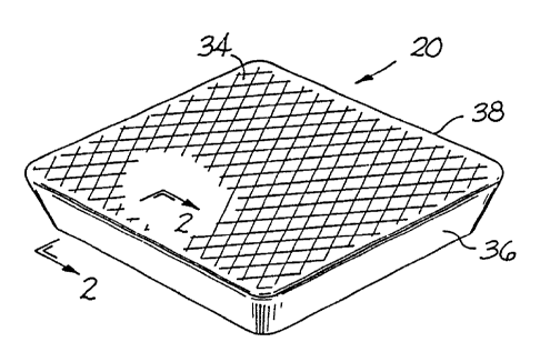
FIGS. 1 and 2 illustrate a first specific
embodiment of the cutting tool of the invention
generally designated as 20. Cutting tool 20 includes a
substrate 22 which has a rake face 24 and a flank face
26. The cutting tool substrate may also be made in any
of the standard shapes and sizes such as those
identified in the American National Standard for
Cutting Tools - Indexable Inserts - Identification
System, ANSI B212.4-1986. Inserts may also have various
chipbreaker structures (not shown) on their rake face
as well to facilitate breakage and removal of chips.
The substrate 22 can be selected from many
possible substrate materials suitable for use as a
cutting tool substrate. Basic material categories
includes tool steels, cemented carbides, cermets,
ceramics, ceramic composites, polycrystalline diamond,
and polycrystalline cubic Boron Nitride as candidates
for a cutting tool substrate.
In the category of cemented carbides, one
substrate is a cobalt cemented tungsten carbide
composition. In these compositions, the cobalt ranges
between about .2 weight percent to about 20 weight
percent with the balance consisting essentially of
tungsten carbide, and optionally, carbides and
carbonitrides with tungsten, titanium, tantalum,
zirconium, hafnium and/or niobium.
In the category of cermets there are titanium
carbonitride-based materials having a cobalt and/or
nickel binder metal. These cermets include the
following grades of cermets sold by Kennametal Inc. of
Latrobe, Pennsylvania (assignee of the present patent
application): KT125, KT150, KT175, and KT195.
CA 02226335 1998-O1-06
WO 97/03777 PCT/US96/06494
-10-
In the category of ceramics there are silicon
nitride-based, or aluminum oxide-based, ceramics with
or without reinforcement additives such as silicon
carbide and titanium carbide in whisker or particulate
form.
In the category of ceramic composites there
are whisker reinforced ceramics. Examples of these
types of composites includes silicon carbide whiskers
and/or titanium carbide whiskers in an alumina matrix.
A coating 28 covers the rake face 24 and the
flank face 26 of the substrate 22. The use of a coating
28 may or may not be necessary depending upon the
specific application and the specific substrate of the
cutting tool. In those cases where coatings are used,
there are many variations for a coating scheme.
A single or multi-layer coating may be
applied by physical vapor deposition techniques. One
such example is a coating of TiAlN or TiN applied by
PVD. One example of a multi-layer coating is a TiN-
TiCN-TiN coating scheme such as that mentioned in U.S.
Patent No. 5,250,367 to Santhanam et al. which
discloses coating schemes that comprise a combination
of CVD and PVD techniques or U.S. Patent 5,075,181 to
Quinto et al. which discloses a multi-layer coating
scheme applied solely by PVD techniques.
Alternatively or in addition to TiAlN,
coating layers may be used for cutting tools include
the carbides, nitrides, carbonitrides and borides of
zirconium, titanium, hafnium and their alloys, alumina,
cubic Boron Nitride, silicon nitride, and a thin film
polycrystalline diamond layer.
Referring back to the substrate 22, the rake
face 24 of the substrate 22 consists of a
microscopically rough surface. The peripheral edge 30
of the substrate 22 is at the joinder of the rake face
24 and the flank face 26. The flank face 26 presents a
relatively smooth surface.
SUBSTITUTE SHEET (RULE 26)
CA 02226335 1998-O1-06
WO 97/03777 PCT/US96/06494
-11-
In regard to the coating 28, coating 28 is
illustrated in the first specific embodiment (FIG. 2)
as a single layer. The coating 28 overlies the
substrate 22 so that the complete coated cutting tool
20 presents an exposed rake face 34 and an exposed
flank face 36. The exposed rake face 34 has a
microscopically rough surface. The exposed flank face
36 presents a relatively smooth surface as compared to
the rake face. The exposed peripheral edge 38 is at the
juncture of the rake face 34 and flank face 36.
The roughness of the rough rake surface 24
for the substrate 22, and for the exposed rake face 34
range between 15 microinches Ra and 125 microinches Ra
as measured on a Sheffield Proficorder Spectre Unit. A
preferable range for this surface roughness is between
microinches Ra and 125 microinches Ra. An even more
preferable range is between 40 microinches Ra and 80
microinches Ra.
Preferably, the roughness of the exposed
20 smooth flank face 36 is less than 25 microinches Ra as
measured on a Sheffield Proficorder Spectre Unit. A
more preferable surface roughness is less than 15
microinches Ra.
The specific embodiment of the cutting tool
25 of FIGS. 1 and 2 presents the advantage of good
adhesion of the coating on the rake face of the
substrate due to the surface roughness of the rake face
of the substrate. This cutting tool has good chip
control due to the surface roughness on the coated rake
face. This specific embodiment also exhibits good
workpiece surface finish characteristics due to the
R
smooth surface of the coated flank face.
Referring to FIGS. 3 through 5, these
drawings illustrate a second specific embodiment of the
cutting tool of the invention generally designated as
42. Cutting tool 42 includes a substrate 44 (see FIG.
5) that presents a rake face 4G and a flank face 48. A
CA 02226335 1998-O1-06
WO 97/03777 PCT/US96/06494
-12-
coating 50 overlies the rake face 46 and the flank face
48. The types of substrates and coatings available for
cutting tool 42 are the same as those available for
cutting tool 20.
The substrate 44 includes a peripheral edge
54 which is at the joinder of the rake face 46 and the
flank face 48. The substrate 44 has a peripheral rough
surface portion 56, i.e., a portion of the surface that
is microscopically rough, which extends inwardly from
the peripheral edge 54 of the substrate 44. A
structural chip breaker 58, which has a microscopically
rough surface, extends inwardly from the inward edge of
the peripheral rough surface portion 56.
The substrate 44 further includes a
microscopically rough central surface portion 60.
Central surface portion 60 is bounded by the structural
chip breaker 58.
The coating 50 (see FIG. 5) overlies the
substrate 44 to form the coated cutting tool 42 that
has an exposed rake face 64 and an exposed flank face
66. The coating 50 has a peripheral edge 70 at the
joinder of the exposed rake face 64 and the exposed
flank face 66 of the coated cutting tool 42.
There is an exposed peripheral
microscopically rough exposed rake face portion 72
that extends inwardly from the peripheral edge 70. An
exposed structural chip breaker 74 then extends
inwardly from the peripheral microscopically rough
exposed rake face portion 72. Structural chip breaker
74 has a microscopically rough surface. The exposed
rake face 64 further includes a central portion 76 that
presents a rough surface. The cutting insert 42
contains a central hole 78.
The roughness of the rake surface portions
(56, 58, 60) of the substrate and of the exposed rake
face portions (72, 74, 76) are the same as described
above for rough rake surface 24. The roughness of the
SUBSTnItIE SHEEC RULE 2R~
CA 02226335 1998-O1-06
WO 97/03777 PCT/US96/06494
-13-
flank 48 surface of the substrate 22 and the exposed
- flank face is the same as described above for the
smooth flank face 36. In another option, the central
. portion 76 of the rake face may have a relatively
smooth surface.
The specific embodiment of FIGS. 3 through 5
presents a cutting tool that has good adhesion of the
coating to the rake face of the substrate because of
the surface roughness of the rake face of the
substrate. This cutting tool has good chip control
properties due to the surface roughness of the coated
rake face of the cutting tool. This cutting tool
presents good workpiece surface finishing properties
due to the smooth surface of the coated flank face.
Referring to FIGS. G and 7, there is
illustrated an uncoated cutting tool generally referred
to as 90. The uncoated cutting tool 90 can be made from
any cutting tool material suitable for use in an
uncoated condition.
The uncoated cutting tool 90 includes a rake
face 92 and a flank face 94. The rake face 92 presents
a microscopically rough surface. The peripheral edge 96
is at the joinder of the rake face 92 and the flank
face 94. The roughness of the rough rake face 92 is the
same as that described above for rough rake surface 24.
The roughness of the flank surface 94 is the same as
that described above for the smooth flank face 36.
The uncoated cutting tool of FIGS. 6 and 7
exhibits good chip control properties due to the rough
surface of the rake face of the cutting tool and
provides smooth workpiece finishes due to the smooth
x
flank surfaces of the cutting tool.
Referring to FIGS. 8 and 9, there is
illustrated another specific embodiment of the cutting
tool of the invention, generally designated as 100.
Cutting tool 100 has a substrate 102 with a rake face
104 and a flank face 106. The rake face 104 is rough,
SUBSIItUIE SHEET (Rlllf 26)
CA 02226335 1998-O1-06
WO 97/03777 PCT/US96/06494
-14-
i.e., has a rough surface microtopography. The flank
face 106 of the substrate also has a rough
microtopography. Cutting tool 100 includes a coating
108 that overlies the surfaces of the substrate 102.
The rake face 110 of the coated cutting tool has a
rough microtopography and the flank face 112 of the
coated cutting tool also has a rough microtopography.
The surface roughness of the coated rake and flank
faces (110, 112) is the same as described above for the
rough rake surface 24.
The specific cutting tool of FIGS. 8 and 9
exhibits good coating adherence to the rake and flank
faces due to the rake and flank faces of the substrate
having a surface roughness. This cutting tool provides
good chip control properties due to the surface
roughness of the coated rake face, but somewhat rougher
workpiece surface finishes due to the surface roughness
of the coated flank faces.
Referring to FIGS. 10 and 11, there is
illustrated another specific embodiment of the cutting
tool of the invention, generally designated as 120.
Cutting tool 120 has a substrate 122 with a rake face
124 and a flank face 126. The rake face 124 is rough,
i.e., has a rough surface microtopography. The flank
face 126 also has a rough microtopography. Cutting tool
100 includes a coating 128 that overlies the surfaces
of the substrate 122. The rake face 130 of the coated
cutting tool has a rough microtopography. The surface
roughness of the rake and flank faces (124, 126) of the
substrate 122 and the coated rake face 130 are the same
as that described above for the rough rake surface 24.
The flank face 132 of the coated cutting tool
has a smooth microtopography. To achieve the smooth
microtopography on the flank face of the coated tool,
the flank face had to be subjected to a polishing or
other treatment to smooth the surface. This is
especially true in light of the fact that the flank
SU~STIiUtE SHEET (RULE 26j
CA 02226335 1998-O1-06
WO 97/03777 PCT/US96/06494
-15-
face of the substrate has a rough microtopography. The
. surface roughness of the coated flank face 132 is the
same as described above for the smooth flank face 36.
The cutting tool of FIGS. 10 and 11 provides
the advantage of good coating adherence to the rake and
flank faces of the substrate due to the surface
roughness of the rake and flank faces of the substrate.
This cutting tool also exhibits good chip control due
to the surface roughness of the coated rake face. The
cutting tool further provides good workpiece surface
finish characteristics due to the smoothness of the
surface of the coated flank face.
Referring to FIGS. 12 and 13, there is
illustrated another specific embodiment of the cutting
tool of the invention, generally designated as 140.
Cutting tool 140 has a substrate 142 with a rake face
144 and a flank face 146. The rake face 144 is rough,
i.e., has a rough surface microtopography. The flank
face 126 has a smooth microtopography. Cutting tool 140
includes a coating 148 that overlies the surfaces of
the substrate 142. The rake face 150 of the coated
cutting tool has a smooth microtopography. The flank
face 152 of the coated cutting tool also has a smooth
microtopography. To achieve the smooth microtopography
on the rake face of the coated tool, the rake face had
to be subjected to a polishing or other treatment to
smooth the surface. This is especially true in light of
the fact that the rake surface of the substrate has a
rough microtopography.
The surface roughness of the rake face 144 of
the substrate is the same as described above for rough
rake surface 24. The surface roughness of the flank
face 146 of the substrate and the coated rake and flank
' faces (150, 152) is the same as described above for the
smooth flank face 36.
The cutting tool of FIGS. 12 and 13 provides
good adherence of the coating to the rake face of the
su~smur~ s~~t (~ut~ 2s~
CA 02226335 1998-O1-06
WO 97/03777 PCT/US96/06494
-16-
substrate due to the surface roughness of the rake face
of the substrate. This cutting tool provides for good
workpiece surface finishing properties due to the
smooth surface of the coated flank face. This cutting
tool also provides for reduced tendency for a built-up
edge on the coated rake face due to the surface
smoothness of the rake face of the coated cutting tool.
Referring to FIGS. 14 and 15, there is
illustrated another specific embodiment of the cutting
tool of the invention, generally designated as 160.
Cutting tool 160 has a substrate 162 with a rake face
164 and a flank face 166. The rake face 164 is rough,
i.e., has a rough surface microtopography. The flank
face 166 has a smooth microtopography. Cutting tool 160
includes a multi-layered coating that overlies the
surfaces of the substrate 162. The coating comprises a
base layer 168, an intermediate layer 170, and a top
layer 172. The rake face 174 of the coated cutting tool
has a rough microtopography. The flank face 172 of the
coated cutting tool has a smooth microtopography.
The surface roughness of the rake face 164 of
the substrate and the coated rake face 174 is the same
as described above for rough rake surface 24. The
surface roughness of the rake face 166 of the substrate
and the coated flank face 176 is the same as described
above for the smooth flank face 36.
The cutting tool of FIGS. 14 and 15 exhibits
good coating adherence to the rake surface of the
substrate due to the surface roughness of the rake face
of the substrate, as well as the surface roughness of
the overlying coating layers. This cutting tool
exhibits good chip control properties due to the
surface roughness of the exposed coated rake face. The
cutting tool has good workpiece surface finishing
properties due to the surface smoothness of the coated
flank face.
SUBSII~ttE SbEEi' (RULE 26)
CA 02226335 1998-O1-06
WO 97/03777 PCT/IJS96/06494
-17-
Referring to FIGS. 16 and 17, there is
illustrated another specific embodiment of the cutting
tool of the invention, generally designated as 180,.
Cutting tool 180 has a substrate 182 with a rake face
184 and a flank face 186. The rake face 184 is rough,
i.e., has a rough surface microtopography. The flank
face 186 also has a rough microtopography. The surface
roughness of the rake and flank faces (184, 186) of the
substrate 182 is the same as that described above for
the rough rake surface 24.
Cutting tool 180 includes a coating 188 that
overlies the surfaces of the substrate 182. The rake
face 190 of the coated cutting tool has a smooth
microtopography. The flank face 192 of the coated
cutting tool also has a smooth microtopography. To
achieve the smooth microtopography on the rake and
flank faces of the coated tool, these faces had to be
subjected to a polishing or other treatment to smooth
the surface thereof. This is especially true in light
of the fact that the rake surface and flank surface of
the substrate has a rough microtopography. The surface
roughness of the coated rake and flank faces (190, 192)
is the same as described for the smooth flank face 36.
The cutting tool of FIGS. 16 and 17 has good
coating adhesion to the rake and flank surfaces of the
substrate due to the rough rake and flank surfaces of
the substrate. This cutting tool has a reduced tendency
for a built-up edge on the coated rake face due to the
surface smoothness of the coated rake face. This
cutting tool provides a good workpiece surface finish
due to the surface smoothness of the coated flank face
of the cutting tool.
In regard to the manufacture of the cutting
tools, the basic substrate is preferably made by
conventional powder metallurgical techniques. More
specifically, the powder components of the substrate
are blended and pressed into a green compact. The green
suesrnurE su~r (RUB 2sj
CA 02226335 1998-O1-06
WO 97/03777 PCT/LTS96/06494
-18-
compact is then subsequently heat treated, such as by
sintering, so as to form a substantially fully dense
substrate (in the case of a coated cutting tool) or the
uncoated cutting tool. In the alternative, a powder
blend can be formed into a substantially fully dense
body by the simultaneous application of heat and
pressure such as, for example, by hot pressing. There
are, however, several variations on the densification
process necessary to form a substrate with the
selective rough surfaces.
One variation of the sintering process of
making the substantially fully dense substrate is to
use a ram that forms the powder into the green compact
which will form the necessary surface roughness in the
green compact. By providing a surface roughness in the
green compact of an appropriate degree and dimension,
there is provided an as-sintered substrate with the
appropriate surface roughness at selected positions on
the surface of the substrate. The use of a ram with the
necessary surface roughness is also available for the
hot pressing process.
If the surface roughness of the as-sintered
(or substantially fully dense) tool is excessive, only
the undesirably rough locations of the tool may be
ground, polished, laser glazed, or otherwise finished
to produce the necessary level of smoothness. This
necessary level of smoothness may, in the case of the
flank face, be sufficient to generate a smooth
workpiece finish in cutting, yet still leave the rough
rake surface of the tool intact to produce the desired
chip-flow control. In the case of the rake face, the
level of smoothness may be sufficient to reduce the
tendency for a built-up edge on the rake face. The
flank surface of the substrate may be in a rough
condition so as to improve the coating adhesion on the
flank surface of the substrate.
SU8~tt1lJTE SS~EEET (RULE 26)
CA 02226335 1998-O1-06
WO 97/03777 PCT/CTS96/06494
-19-
Depending on the tool material and cutting
application, the tool may be used as-is in the above
described condition. In other words, the tool may be
used in an uncoated condition. More commonly, however,
this tool will serve as a substrate for a protective
wear-resistant coating applied by CVD or PVD methods
and then used in the cutting application.
The coating process parameters as known to
those skilled in the art are such that the roughness
characteristic of the rake and flank surfaces of the
tool may be unchanged from that of the substrate prior
to the coating operation. In general, however, for the
typical CVD and PVD coating processes, the surface
roughness of the coated tool is a function of the
roughness of the underlying substrate surface and the
thickness of the deposited coating. Generally speaking,
as the coating thickness increases, the surface
roughness of the coating also tends to increase
regardless of the underlying surface roughness of the
substrate. This could result in the exposed coated
surfaces somewhat rougher than the surfaces of the
substrate, however, such an increase in surface
roughness of the rake surface of the substrate is not
deleterious to the desirable chip control properties.
The increase in surface roughness of the substrate does
not negatively impact on the adhesion of the coating to
the substrate, but will typically improve the adhesion.
An increase in surface roughness of the
coated flank surface of the tool, however, could
adversely affect the workpiece surface finish generated
by the tool. For this reason, a post coating operation
such as polishing, buffing, or laser glazing all of
some of the flank surfaces of the tool may be required
to smooth the surface of the coating to an acceptable
surface smoothness, thus, providing acceptably smooth
workpiece finishes in the cutting operation.
SUBSIiTUTE SHEET tRULE 26~
CA 02226335 2003-04-28
68188-114
-20-
An increase in the surface roughness of the coated
rake surface may generate a problem of a built up edge,
i.e., material from the chip is welded to the rake surface
of the cutting tool. To reduce the potential for a problem
of a built up edge, a post coating operation such as
polishing, buffing, or laser glazing all or some of the rake
surfaces of the tool may be required to smooth the surface
of the coating to an acceptable surface smoothness, thus,
reducing the potential for the occurrence of a built up
edge. The built-up edge is a problem that is workpiece
material dependent. While smoothing the rake surface
reduces chip control properties, it still leaves the coating
with good adhesion due to the surface roughness of the rake
face of the substrate.
Still another variation on the basic process uses
an additional resintering step after the initial processing
of the substrate. The purpose of the resintering is to
enlarge the grains of the substrate, e.g., tungsten carbide,
at the surface so as to form a rough irregular surface. The
irregular surface presents a surface with the necessary
roughness. This process is a subject of a United States
patent/5,585,176 issued Dec. 17, 1996 and entitled DIAMOND
COATED TOOLS AND PROCESS FOR MAKING.
In this variation that uses resintering in
conjunction with the cemented tungsten carbide substrate,
the surface of an as-sintered tungsten carbide based
cemented carbide substrate is composed of tungsten carbide
hard grains bound together by cobalt or a cobalt alloy. The
cobalt is not only between the tungsten carbide grains, but
also covers some of the
CA 02226335 1998-O1-06
WO 97/03777 PCT/US96/06494
-21-
tungsten carbide grains at the substrate surface due to
the wetting properties of Co and tungsten carbide under
vacuum sintering conditions.
Now in accordance with the present invention,
the as-sintered and ground substrate described above is
now resintered under time, temperature and atmospheric
conditions, to cause grain growth and binder depletion
from its surfaces. The time and temperature are
selected such~that sufficient grain growth occurs on
the surface of the resintered substrate to produce a
surface roughness, Ra, in the ranges set out above for
the rough rake surface 24.
The resintering times required to achieve the
required surface roughness will depend on the starting
material and the sintering conditions. As temperature
increases, resintering times should decrease. For some
cemented tungsten carbide compositions, resintering
times of 2 to 3 hours at 1510°C (2750°F) have been
found to be sufficient to provide the needed surface
roughness. If the desired surface roughness is not
produced after the first resintering treatment, the
substrate may be resintered again until the desired
surface roughness is produced.
It is believed that the atmosphere during the
resintering treatment may also be important to
obtaining good coating adhesion to the substrate. It
is believed that if a nitrogen atmosphere is utilized
during this treatment, the amount of cobalt on the
resulting rough surface will be minimized. The
nitrogen partial pressure should be controlled to allow
cobalt evaporation from the surface. During the
resintering one should minimize re-wetting of the
surface by additional cobalt from the bulk of the
substrate.
The most beneficial nitrogen partial pressure
may, therefore, be a function of the substrate
composition. Nitrogen partial pressure may also be
CA 02226335 1998-O1-06
WO 97/03777 PCT/LTS96/06494
-22-
controlled or varied during the resintering cycles) to
control the amount and rate of cobalt evaporation from
the bulk of the substrate. It is believed that a 0.3 to
50 torr, preferably, 0.3 to 5, and more preferably, 0.3
to 2 torr nitrogen atmosphere should be utilized. It
is theorized that the nitrogen atmosphere may allow
cobalt on the exterior surfaces of the grains on the
substrate surface to evaporate, while sufficient cobalt
remains between the surface tungsten carbide grains to
keep them well bonded to the remainder of the
substrate. Cobalt surface evaporation is accompanied
by tungsten carbide grain growth at the surface,
resulting in surface roughening.
After the completion of the resintering
process, the substrate may then be coated by physical
vapor deposition techniques, chemical vapor deposition
techniques, or a combination of techniques that
includes physical vapor deposition techniques. The tool
in this condition may be CVD or PVD coated prior to
use. If the as-resintered tool is coated directly, the
outermost surface of the coating on flank surfaces will
preferably be smoothed by polishing, buffing, laser
glazing, or the like in the zone that comes in contact
with the workpiece in order that the tool generates the
smoothest workpiece surface finish in the cutting
operation.
In regard to the surface roughness of the
coated cutting tool, the roughness of the rake surface
has the same ranges as set out above for the rough rake
surface 24. As described above, peripheral grinding,
polishing, buffing, or laser glazing the flank surface
of the tool will smooth the flank surface while leaving
the rough rake surface intact. Typically, the flank
face is subjected to buffing so that the roughness of
the flank surface is in the same ranges set out above
for the smooth flank face 36.
su~rtnrrF s~~r ~ua~ zs~
CA 02226335 1998-O1-06
WO 97/03777 PC'T/US96/06494
-23-
Still another variation on the process of
making the basic substrate is to grind, EDM (electric
discharge machine), or laser etch a surface roughness
into the as-sintered substrate at selected positions on
the surface of the rake face. For all of the variations
set forth above, if the surface of the flank face of
the as-sintered substrate is sufficiently smooth then
no further processing is necessary. Typically, if the
cutting tool is coated, it is the coating on the flank
1o surface that will be polished, buffed, or laser glazed
to achieve the necessary smoothness.
While cutting tools, especially those made
from cemented tungsten carbide, are typically
fabricated by cold pressing and vacuum (i.e., at a
pressure of about 10-2 to 10-3 torr) sintering
techniques, it should be understood that any of
conventional techniques may be used to obtain the basic
as-sintered substrate for the present invention.
Examples
In order to demonstrate the advantages and
benefits provided by the present invention, a number of
examples, and the results of testing of such examples,
are set forth hereinafter.
For all of the examples which are set forth
below, unless designated otherwise, the starting
substrate was a cobalt cemented tungsten carbide of the
following composition and properties: 2.3 to 2.9 weight
percent Co: up to 0.4 weight percent Ta; up to 0.1
weight percent Ti; up to 0.1 weight percent Nb and
other impurities; and the balance being WC. Other
properties of the as-sintered substrate were a Rockwell
A hardness between 92.8 and 93.6, a coercive force, Hc,
between 290 and 440 oersteds, a magnetic saturation
sufficient to avoid the formation of eta phase, the
average WC grain size was between 1-6 micrometers, the
porosity rating was A08, BOO, Coo or better, and the
density was between 15.10 to 15.50 grams/cc.
suBSnru~ s~~ ~u~ Zs~
CA 02226335 1998-O1-06
WO 97/03777 PCT/US96/06494
-24-
For all of the examples, the cutting tool
that was used was a SPG-422 (.0005 inch radius hone)
style of tool, which did not have a structural chip
breaker.
For those examples that were subjected to
resintering, the resintering was performed at 2750°F
for three hours in about 0.5 torr nitrogen atmosphere
to produce a surface roughness of above 45 microinches
Ra. Resintering of the as-sintered and ground substrate
typically results in the reduction of the cobalt
content in the resintered substrate due to cobalt
evaporation at the surface during the resintering
process.
For those examples that were subjected to
buffing, the buffing was performed for two minutes per
edge using a nylon brush whose bristles were
impregnating with 120 mesh diamond grit rotating at a
speed of 1000 rpm. The brush is available from Jason,
Inc. of Cleveland, Ohio.
To evaluate the adherence of various coatings
to the substrate of the cutting tool, the following
examples; namely, Examples EB46, CN88, CN89, EB56,
C007, C008, EB66, CQ87, and C988~ were tested for
coating adherence using an indentation adhesion load
test. In this regard, adhesion between the coating and
the substrate was determined by an indentation adhesion
test using a Rockwell hardness tester with a Rockwell A
scale Brale cone shaped diamond indenter at a selected
load range of l5kg, 30kg, 45kg, 60kg and 100kg. The
adhesive strength was defined as the minimum load at
which the coating debonded and/or flaked. Measurements
were performed at two sites on the inserts. The
measurements of "100 +" indicate that the coating did
not debond or flake at the load of 100kg, which was the
maximum load used in these tests.
A description of these examples is set forth
below.
suesnrurE sbE~r (RUtF 2s)
CA 02226335 1998-O1-06
WO 97/03777 PCT/US96/06494
-25-
Example EB46 comprised the basic as-sintered
cemented tungsten carbide substrate with a TiAlN
coating applied via PVD for 4 hours in a CC800 reactor
from CemeCon GmbH of Aachen, Germany. This reactor used
a magnetron sputtering process to apply the TiAlN. The
TiAlN coating had a thickness of about 3.5 micrometers.
This example presented one embodiment of the invention
wherein a thin single layer coating was applied via PVD
to the as-ground substrate.
Example CN88 comprised the basic as-sintered
and ground substrate that was subjected to a
resintering as described above prior to the application
of the TiAlN coating to a thickness of about 3.5
micrometers in the same coating run as for Example
EB46. Example CN88 was an embodiment of the invention
wherein the substrate was subjected to resintering
prior to the application of the thinner TiAlN coating.
Example CN89 was the same as Example CN88.
Example EB56 comprised the basic as-sintered
and ground cemented tungsten carbide substrate with a
TiAlN coating applied via PVD for 10 hours in the CC800
reactor from CemeCon GmbH of Aachen, Germany. The TiAlN
coating had a thickness of about 10.5 micrometers. This
example was an embodiment of the invention wherein a
thicker single layer coating was applied via PVD to an
as-ground substrate.
Example C007 comprised the basic substrate
that was subjected to a resintering (as described
above) prior to the application of the TiAlN coating to
a thickness of about 10.5 micrometers in the same
coating run as for Example EBSG. Example C007 was an
embodiment of the invention wherein the substrate was
subjected to resintering prior to the application of
the thicker TiAlN coating.
Example C008 was the same as Example C007.
Example EB6G comprised the basic as-sintered
and ground cemented tungsten carbide substrate with a
Sl~~!~ S~~ET ~UL~ 26~
CA 02226335 1998-O1-06
WO 97/03777 PCT/US96/06494
-26-
multi-layer coating applied via a combination of CVD
and PVD. The coating scheme comprised: the application
by CVD of a base layer of TiN that was about 1.0
micrometers thick; the application by CVD of an
intermediate layer of TiCN that was about 4.0
micrometers thick, and the application by PVD of a top
layer of TiN that was about 4.0 micrometers thick. This
example presented one embodiment of the invention
wherein a multi-layer coating was applied via CVD and
PVD to an as-ground substrate.
Example CQ87 comprised the basic substrate
that was subjected to a resintering (as described
above) prior to the application of the multi-layer
coating in the same coating run as for Example EB66.
Example CQ87 was an embodiment of the invention wherein
the substrate was subjected to resintering prior to the
application of the multi-layer coating.
Example CQ88 was the same as Example CQ87.
The results of the indentation load testing
in kilograms is set forth below in Tables I through
III. Two measurements were taken for each cutting tool.
A higher indentation load test result equates to better
coating adherence.
Table I
Indentation Load Test Results for
Substrate with a 3.5 ~,m TiAlN PVD Coating
Example Condition of the Indentation Load
Substrate (kg) at Failure
EB46 as-ground 45, 60
CN88 resintered 100+, 100+
CN89 resintered 100+, 100+
SUBS1IIU~E SHEET (RULE 26)
CA 02226335 1998-O1-06
WO 97/03777 PCT/US96/06494
-27-
Table II
Indentation Load Test Results for
Substrate with a 10.5 /Cm TiAlN PVD Coating
Example Condition of the Indentation Load
Substrate (kg) at Failure
EB56 as-ground 30, 30
C007 resintered 60, 60
C008 resintered 100+, 100+
Table III
Indentation Load Test Results for
Substrate with a CVD-PVD Coating
Example Condition of the Indentation Load
Substrate (kg) at Failure
EB66 as-ground 60, 60
CQ87 resintered 45, 60
CQ88 resintered 45, 45
Three samples of a conventional prior art
cutting tool (KC730) coated with TiN to a thickness of
about 3.5 micrometers by ion plating on a cemented
carbide substrate containing about 6 weight percent
cobalt were tested for the indentation adhesion load,
and the results of two measurements per cutting tool
were 30kg, 45kg for each one of the three cutting
tools.
Referring to Table I, the indentation load
results show that for cutting tools having a thinner
(about 3.5 micrometer) PVD coating of TiAlN, the
adherence of the coating showed significant improvement
for those cutting tools having substrates that were
resintered after initial sintering and prior to
coating. In this regard, Sample Nos. CN88 and CN89
each showed indentation load results of 100+Kg as
compared to sample EB46 which had indentation adhesion
load measurements of 45kg and 60kg. A comparison of the
SUBSTIO1IE SHEET' (RULE 26)
CA 02226335 1998-O1-06
WO 97/03777 PCT/LTS96/06494
-28-
results of Table I against those for the KC730 cutting
tool show that the adhesion of the thinner TiAlN
coating (samples CN88 and CN89) improves more than two
to three times over that of a comparable conventional
cutting tool (KC730) when the substantially fully dense
substrate is resintered prior to coating.
Referring to Table II, the indentation load
results show that the adherence of a thicker (about
10.5 micrometers) coating of TiAlN applied via PVD
techniques to an as-ground tool is about the same as
that of a conventional cutting tool (KC730) as measured
in accordance with the indentation load test. The
adherence, of the thicker PVD coating is significantly
improved over that of the conventional KC730 cutting
tool when the substantially fully dense substrate has
been resintered before coating.
Referring to Table III, the indentation load
results show that for the multi-layer coating [CVD-
TiN/CVD-TiCN/PVD-TiN] there is no significant
difference in the indentation adherence load test
results between the cutting tools with an as-ground
substrate and the cutting tools with a resintered
substrate.
Overall, it is apparent that for the cutting
tools having the single layer of TiAlN, whether it is
about 3.5 micrometers thick or about 10.5 micrometers
thick, the resintering of the as-ground substrate
significantly improves the coating adhesion strength.
The resintering of the as-ground substrate for cutting
tools with a CVD-PVD coating does not appear to
significantly improve the adherence of the coating to
the substrate.
Samples of certain ones of the above cutting
tools, as well as two conventional cutting tools, were
used to turn 383.2 aluminum (11 weight percent silicon)
alloy under the following conditions: speed of 2500
sfm, feed of .005 inches per revolution, depth of cut
SUBS~'ttUTE SHEET ~RUtE 26~
CA 02226335 1998-O1-06
WO 97/03777 PC'aYUS96/06494
-29-
of .025 inches, and flood coolant. The results of the
these turning test are set forth below in Table IV.
Table IV
Chip Formation Test Results
Example Condition of the Chip Character
Substrate (FIG. that shows
the chips)
Uncoated as-ground, no long continuous
Substrate coating stringers, "birds
t'
KC730 Cutting as-ground long
continuous
Tool stringers, "birds
nest"
cutting Tool like as-ground long continuous
EB46 ( 3.5 ~m stringers, "birds
TiAlN coating) nest" (FIG. 20A)
Cutting Tool like resintered short coils
CN88 ( 3.5 ~m
(FIG.20B)
TiAlN coating)
Cutting Tool like as-ground long continuous
EB66 (CVD-PVD stringers, "birds
coating scheme) nest" (FIG. 21A)
Cutting Tool like resintered short coils
CQ87 (CVD-PVD (FIG.21B)
coating scheme)
Referring to Table IV, the test results for
turning 383.2 aluminum alloy reveal that the use of the
substrate that had been resintered provides for much
improved chip formation properties. The cutting tools
that used resintered substrates, whether in conjunction
with a single thin layer (about 3.5 micrometers) of
TiAlN or in conjunction with a multi-layer coating
scheme, formed chips in the form of short coils. The
short coil style of chip is a desirable chip style.
This is shown in a dramatic fashion for the
single thin layer of TiAlN by a comparison of FIG. 20A
with FIG. 20B. FIG.. 20A is a photograph that shows the
undesirable long continuous stringer type of chips.
This is in significant contrast to FIG. 20B which shows
the tight, short coil type of chip.
CA 02226335 1998-O1-06
WO 97/03777 PCT/US96/06494
-30-
A comparison of FIG. 21A and 21B also shows
the significant difference in chip formation between
the CVD-PVD coated cutting tools having the as-ground
substrate or the resintered substrate. FIG. 21A is a
photograph that shows long stringers generated with
turning using the coated cutting tool with the as-
ground substrate. FIG 21B is a photograph that shows
the tight, short coil style chips generated while
turning using the coated cutting tool having the
resintered substrate.
The formation of short coils for those
cutting tools having a resintered substrate was also in
contrast to the chip formation of the conventional
uncoated K11 substrate cutting tool and the
conventional coated KC730 cutting tool. FIG. 19 is a
photograph that shows the long continuous stringer
chips formed when turning using an uncoated K11
substrate cutting tool. It is very apparent that a
cutting tool with a resintered substrate, wherein the
rake face has the requisite surface roughness, provides
for much improved chip formation properties over a
cutting tool with an as-ground substrate in the turning
of 383.2 aluminum alloy.
Applicant believes that a cutting tool with
the requisite rake surface roughness has particularly
good application for chip control when used to machine
so-called "gummy" workpiece materials. These workpiece
materials include aluminum-based alloys, magnesium-
based alloys, copper-based alloys, brass alloys, and
mild steel alloys such as, for example, AISI 1008 and
AISI 1045 steels.
Turning tests on 383.2 aluminum alloy under
the conditions set forth above was also performed using
Examples EB46 and CN82. The results of these tests are
set forth in Table V below. FIG. 18 shows a view of the
cutting tool A-CN82 (resintered with 3.5 ~,m TiAlN) so
as to illustrate the four corners of the cutting tool
~usbE~r (RU~zs)
CA 02226335 1998-O1-06
WO 97/03777 PC:T/LTS96/06494
-31-
including corners 2 and 4. The flank face of the
cutting tool was buffed at corner 4 after coating. The
remainder of the cutting tool was not buffed.
' Table V
Surface Roughness Characteristics of
Cutting Tools and the Workpiece Surface Finish
Tool Surface Tool Surface Buffed After
Material Condition Coating
Prior to
Coating
A-EB46 As-ground Rake No
Flank No
A-CN82 Resintered Rake No
(Corner 2) Flank
No
A-CN82 Resintered Rake No
(Corner 4) Flank Yes
Tool Coating Coating Workpiece Chip
Material Surface Surface Surface Character
Roughness Roughness Finish
(/.cinches (/cinches (,inches
Ra) Rtm) Ra)
A-EB46 9 (r) 142 (r) 427 Long
11 (f) 165 (f) continuous
stringers
A-CN82 55 (r) 354 (r) 484 Short
(Corner 80 (f) 387 (f) Coils
2)
A-CN82 54 (r) 348 (r) 312 Short
(Corner 8 (f) 55 (f) Coils
4)
In the coating surface roughnesses reported
in Table V above, the use of the "(r)" means the
roughness on the rake face of the cutting tool, and the
"(f)" means the roughness on the flank face of the
cutting tool.
Referring to Table V, the cutting tool that
had the resintered substrate with the thin PVD TiAlN
coating (CN82) formed short coil style chips in
StIBSif IUIE SHEEP (RULE 26)
CA 02226335 1998-O1-06
WO 97/03777 PCT/US96/06494
-32-
contrast to a cutting tool with an as-ground substrate
and the thin PVD TiAlN coating. The roughness of the
coating surface is greatest for those surfaces of the
resintered substrate wherein the coating was not
buffed. For example, the rake and flank surfaces of the
as-ground coated cutting tool had surface roughnesses
of 9 and 11 microinches Ra, (142 and 165 Microinches
Rtm) respectively. This is in comparison to the surface
roughness of the coating of a resintered substrate not
subjected to buffing which were between 54 and 60
microinches Ra (348 and 387 microinches Rtm).
Buffing the flank face of the cutting tool
with the resintered substrate did much to smooth the
surface and therefore decrease the surface roughness. A
comparison between opposite corners of sample CN82
shows that buffing decreased the surface roughness of
the coating from 60 to 8 microinches Ra (387 to 55
microinches Rtm)
Buffing the flank face also resulted in a
smoother workpiece surface finish. In this regard, the
workpiece surface finish from the as-ground cutting
tool was 42~7 microinches Ra and the workpiece surface
finish from the resintered cutting tool was 48~4
microinches Ra. These surfaces finishes are in contrast
to 31~2 microinches Ra for the cutting tool
(CN82/Corner 4) having the buffed flank surface.
The examples described below; namely,
Examples EB46-AL, CN89-RL, CN89-RLB, EB56-AH, C008-RH,
C008-RHB, EB66-A, CQ87-R and CQ87-RB, were used to turn
304 stainless steel under the following conditions:
speed of 800 sfm, feed of .008 inches per revolution,
depth of cut of .060 inches, flood coolant, and a 15°
lead angle.
Example EB46-AL comprised the basic as-
sintered cemented tungsten carbide substrate with a
TiAlN coating applied via PVD for 4 hours to a
thickness of about 3.5 micrometers. This example
suesmurE s~~r ~u~ zs~
CA 02226335 1998-O1-06
WO 97/03777 PCT/~JS96/06494
-33-
presented one embodiment of the invention wherein the
thinner single layer coating was applied via PVD to the
as-ground substrate.
Example CN89-RL comprised the basic substrate
f
that was subjected to a resintering prior to the
application of the TiAlN coating to a thickness of
about 3.5 micrometers in the same coating run as for
Example EB46. Example CN89-RL is an embodiment of the
invention wherein the substrate is resintered prior to
the application by PVD of the thinner single layer
coating.
Example CN89-RLB comprised the basic
substrate that was subjected to resintering prior to
the application of the TiAlN coating to a thickness of
about 3.5 micrometers in the same coating run as for
Example EB46. Example CN89-RLB was then subjected to
buffing of the flank face. Example CN89-RLB was an
embodiment of the invention wherein the substrate was
resintered, coated with a single PVD layer, and the
flank face of the coated cutting tool buffed.
Example EB56-AH comprised the basic as-
sintered cemented tungsten carbide substrate with a
TiAlN coating applied via PVD for 10 hours to a
thickness of about 10.5 micrometers. This example
presented one embodiment of the invention wherein a
thicker single layer coating was applied via PVD.
Example C008-RH comprised the basic substrate
that was subjected to a resintering prior to the
application of the TiAlN coating to a thickness of
about 10.5 micrometers in the same coating run as for
Example EB56-AH. Example C008-RH was an embodiment of
the invention wherein the substrate is subjected to
resintering prior to the PVD application of the thicker
TiAlN coating.
Example C008-RHB comprised the basic
substrate that was subjected to a resintering prior to
the application of the TiAlN coating to a thickness of
su~s~rourE sir ~u~ zs~
CA 02226335 1998-O1-06
WO 97/03777 PCT/US96/06494
-34-
about 10.5 micrometers in the same coating run as for
Example EB56-AH. The flank face of the coated tool was
then subjected to buffing. Example C008-RHB was an
embodiment of the invention wherein the substrate was
subjected to resintering prior to the application of
the TiAlN coating, and then the flank face of the
coated tool was buffed.
Example EB66-A comprised the basic as-
sintered cemented tungsten carbide substrate with a
multi-layer coating applied via a combination of CVD
and PVD. The coating scheme comprised: the application
by CVD of a base layer of TiN that was about 1.0
micrometers thick; the application by CVD of an
intermediate layer of TiCN that was about 4.0
micrometers thick, and the application by PVD of a top
layer of TiN that was about 4.0 micrometers thick. This
example presents one embodiment of the invention
wherein a multi-layer coating is applied via CVD and
PVD to an as-ground substrate.
Example CQ87-R comprised the basic substrate
that was subjected to a resintering prior to the
application of the multi-layer coating by CVD and PVD
in the same coating run as for Example EB66-A. Example
CQ87-R is an embodiment of the invention wherein the
substrate is subjected to resintering prior to the
application of the multi-layer coating.
Example CQ87-RB comprised the basic substrate
that was subjected to a resintering prior to the
application of the multi-layer coating by CVD and PVD
in the same coating run as for Example EB66-A. The
flank face of the coated tool was then subjected to
buffing. Example CQ87-RB was an embodiment of the
invention wherein the substrate was subjected to
resintering prior to the application of the multi-layer
coating, and then the flank face of the coated tool was
buffed.
CA 02226335 1998-O1-06
WO 97/03777 PCT/US96/06494
-35-
The results of the turning tests for the 304
stainless steel are set forth below in Tables VI
through VIII.
Referring to the left-hand column of the
tables, the designations for the "Condition°' of the
tool have the following meanings. The designation "A"
means that the cutting tool had an as-ground substrate
prior to the coating process. The designation '°R" means
that the cutting tool had an as-ground substrate that
was resintered prior to the coating process. The
designation "R & B" means that the cutting tool had an
as-ground substrate that was resintered prior to the
coating process and the coated flank face of the
cutting tool was buffed.
Referring to the row identified as °'Tool Life
& Failure Mode", the tool life is measured in minutes.
If the cutting tool remained useful, i.e., did not
satisfy a pre-selected failure criterion, after 40
minutes of turning, the test was stopped and the tool
life recorded as 40.0+ minutes with no failure
occurring. If the cutting tool satisfied one of the
pre-selected failure modes, then the tool life at the
time of failure was recorded in minutes along with the
particular mode of failure. The failure modes are
described below.
The uniform flank wear ("fw") failure mode
occurred when the uniform flank wear reached .015
inches. The maximum localized flank wear ("mw") failure
mode occurred when the maximum localized flank wear
reached .030 inches. The maximum crater depth ("cr")
failure mode occurred when the maximum crater depth as
measured from the surface of the rake face reached .004
inches. The maximum depth-of-cut notch ("dn") failure
mode occurred when the depth-of-cut notch reached .030
inches. The maximum chipping ("ch") failure mode
occurred when the size of the chip reached .030 inches.
The designation "bk" means that the cutting tool broke.
SUBSItIItIE SHEET (RULE 26)
CA 02226335 1998-O1-06
WO 97/03777 PCT/US96/06494
-36-
Referring to the row designated as "Condition
at 40 minutes", this row reflects the condition of the
cutting tool at the end of 40 minutes of turning
assuming that the cutting tool was turning at the 40
minute point in the test. This row indicates the
condition and the extent of wear for that condition in
one-thousandths of an inch.
The corner flaking rating is a numerical
rating that rates the extent of corner flaking of the
coating. The flank flaking rating is a numerical rating
that rates the extent of flank flaking of the coating.
For both of these ratings, the rating of "5" means that
there was no flaking of the coating. The rating of "3"
means that there was noticeable flaking. The rating "1"
means that there was severe flaking of the coating. The
rating "4" is between ratings "5" and "3", and the
rating "2" is between ratings "3" and "1".
The chip flow rating is a numerical rating
that rates the extent of chip flo~-r damage to the
coating. The rating "5" means that there was no damage
due to chip flow. The rating "3" means that there was
noticeable damage due to chip floso. The rating "1"
means that there was severe chip flow damage. The
rating "4" is between ratings "5" and "3". The rating
"2" is between ratings "3" and "1".
SUBSTI~U1E SHEEI (RULE 26)
CA 02226335 1998-O1-06
WO 97/03777 PCT/US96/06494
-37-
Table VI
Test results for the Turning of 304
Stainless Steel for Cutting Tools of the
Substrate with 3.5 /.t,m TiAlN PVD Coating
Example EB46-AL CN89-RL CN89-RLB
Condition A R R & B
Tool Life & 40.0+ 10.0 fw 2.0 ch
Failure Mode
Condition at 1.8 (fw) - -
40 minutes
4.1 (mw)
Corner 3 5 5
Flaking
Rating
Flank 4 5 5
Flaking
Rating
Chip Flow 5 5 4
Rating
Average 114 124 100
Surface
Finish
(/.cinches
Ra)
High Surface 133 124 108
Finish
(,inches Ra)
Low Surface 102 124 g7
Finish
(/Cinches Ra)
CA 02226335 1998-O1-06
WO 97/03777 PCT/US96/06494
-38-
Table VII
Test results for the Turning of 304
Stainless Steel for Cutting Tools of the
Substrate with 10.5 ~Cm TiAlN PVD Coating
Example EB56-AH C008-RH CO08-RHB
Condition A R R & B
Tool Life & 40.0+ 14.0 (mw) 20.0 bk
Failure Mode
Condition at 11.2 (fw) - -
40 minutes
15.4 (mw)
Corner 1 5 5
Flaking
Rating
Flank Flaking 2 5 5
Rating
Chip Flow 5 3 3
Rating
Average 89 148 108
Surface
Finish
(inches Ra)
High Surface 113 191 114
Finish
(,inches Ra)
Low Surface 76 85 100
Finish
(,inches Ra)
~!lBSiIII~IE SNEE1' (RULE 26)
CA 02226335 1998-O1-06
WO 97/03777 PCT/US96/06494
-39-
Table VIII
Test results for the Turning of 304
Stainless Steel for Cutting Tools of the
Substrate with CVD-PVD Coating
Example EB66-A CQ87-R CQ87-RB
Condition A R R & B
Tool Life 40.0+ 40.0 ch 40.0+
&
Failure Mode
Condition 1.7 (fw) 2.6 (fw) 4.8 (fw)
at
40 minutes
3.2 (mw) 5.2 (mw) 11 (mw)
Corner 4 5 5
Flaking
Rating
Flank 5 5 5
30 Flaking
Rating
Chip Flow 4 1 2
Rating
Average 85 123 46
Surface
Finish
(inches Ra)
High Surface 94 137 53
Finish
(inches Ra)
Low Surface 82 88 35
Finish
(inches Ra)
The conventional KC730 cutting tool had a
tool life of 2.0 minutes and the failure mode was
chipping. The corner flaking rating was 2, the flank
flaking rating was 5, and the chip flow damage rating
was 4. The conventional uncoated K11 cutting tool had a
SUBSTttt~TESHEE~ (RULE26)
CA 02226335 1998-O1-06
WO 97/03777 PCT/US96/06494
-40-
tool life of 0.4 minutes and the failure mode was
breakage. The chip flow damage rating was 4.
Referring to Table VI, the cutting tools
having the as-ground substrate with a single thin (3.5
micrometers) PVD layer of TiAlN experienced much
greater tool life in the turning of 304 stainless steel
than the conventional cutting tool and the cutting
tools having the resintered substrate. The as-ground
cutting tool (EB46-AL) had a tool life of 40+ minutes
as compared to 10 minutes and 2 minutes. The cutting
tools that had the resintered substrate had the best
ratings for corner flaking, flank flaking, and chip
flow damage as compared to the cutting tools with the
as-ground substrate. The average workpiece surface
finish was higher, i.e., rougher, for the cutting tool
with a resintered substrate. Buffing the flank of the
cutting tool with the resintered substrate helped
reduce the roughness of the workpiece surface finish.
Referring to Table VII, the cutting tools
having the as-ground substrate with the single thick
(10.5 micrometer) PVD layer of TiAlN experienced much
greater tool life in the turning of 304 stainless steel
than the conventional cutting tool. The cutting tools
with the resintered substrate and the single thick PVD
layer of TiAlN experienced greater tool life than the
conventional cutting tool, but less tool life than the
as-ground cutting tools. The resintered cutting tools
had a better corner flaking rating and flank flaking
rating than the as-ground cutting tools. The as-ground
cutting tools had the best chip flow damage rating. The
as-ground cutting tool resulted in workpiece surface
finishes that were the smoothest. The resintered
cutting tools had the roughest workpiece surface
finishes. Buffing reduced the workpiece surface
roughness (C008-RHB).
Referring to Table VIII, the cutting tools
with the multi-layer coating experienced improved tool
SUB~'(fUTE SBEET (RULE 26)
CA 02226335 1998-O1-06
WO 97/03777 PCT/US96/06494
-41-
life over that of the conventional cutting tool. The
resintered cutting tools had excellent corner flaking
and flank flaking ratings. The as-ground cutting tool
had the best chip flow damage rating while the other
cutting tools had lower ratings. The resintered cutting
tools subjected to buffing produced workpieces with the
smoothest surface finishes. The resintered cutting
tools produced workpieces with the roughest surface
finishes.
Referring again to Table VI through VIII,
these cutting tools having a low cobalt ( 2.9 weight
percent) substrate experienced outstanding tool life in
the turning of 304 stainless steel. More specifically
Example EB46-AL (as-ground low cobalt substrate/ 3.5~Cm
TiAlN PVD coating) had a tool life of 40.0+ minutes
with no failure. Example EB56-AH (as-ground low cobalt
substrate/ 10.5 ~,m TiAlN PVD coating) had a tool life
of 40.0+ minutes with no tool failure. Example EB66-A
(as-ground low cobalt substrate/CVD-PVD coating) had a
tool life of 40.0+ minutes with no failure. Example
CQ87-R (resintered low cobalt substrate/CVD-PVD
coating) had a tool life of 40.0 minutes with failure
by chipping. Example CQ87-RB (resintered and buffed low
cobalt substrate/ CVD-PVD coating) had a tool life of
40.0+ minutes with no failure. Very clearly, the use of
a low cobalt-WC substrate with any one of the coating
schemes results in a tool life that surpasses the
comparable conventional cutting tools (KC730 and
uncoated K11).
The coating schemes as set forth in the
specification herein have application for use with
substrates that present a binder-enriched peripheral
layer. When used with the binder-enriched substrates,
these coating schemes should have the same advantages
and beneficial results that exist with respect to the
low cobalt substrates as set forth in this
specification.
CA 02226335 1998-O1-06
WO 97/03777 PCT/US96/06494
-42-
Other specific embodiments of the invention
will be apparent to those skilled in the art from a
consideration of this specification or practice of the
invention disclosed herein. It is intended that the
specification and specific embodiments be considered as
exemplary only, with the true scope and spirit of the
invention being indicated by the following claims.
SUBSTttUU~'E S~E~" ~RUt~ 2G~