Note: Descriptions are shown in the official language in which they were submitted.
CA 02226617 1998-01-12
W O 97/04424 PCT/GB96/00804
- 1 -
Coin V~lic1~tQr
Field of the Invention
The present invention relates to a coin validator.
Background to the Invention
US-A-4 474 281 t~icçloses a coin validation apparatus wherein a pair of optical
beams are directed across the coin path of a validator, sllhst~nti~lly in the
plane of a coin under test. The optical beams are spaced along the direction
10 of travel of a coin in the coin path. The ~ mt ter of a coin is determin~-(l by
timing the periods during which each of the optical beams is interrupted by a
passing coin, determining a value for the speed of the coin as it crosses the
bearns, deriving two ~ mPter values from the timed periods and the speed
values, and avcld~;hlg the resl.h~nt values. The average produced is
~5 proportional to the rii~m~ter of the coin interrupting the beams.
If the apparatus of US-A-4 474 281 is to function correctly, a coin to be testedmust be in free fall before it encounters the first optical beam. A problem
arises from this in that it is ~liffic~lt to produce a compact validator with a
20 s.lffi~ient run-in for a coin to be in free fall, before it ill~CllUp~ the first
optical beam. The problem is particularly acute in the case of validators for
the large tokens used in some casinos.
DE-A-2 724 868 discloses an apparatus in which the rli~mlot~or of a coin is
25 rherk~l on the basis of the time between the leading edge of the coin
re~hing a lower reference and the trailing edge of the coin leaving an upper
reference position. However, this apparatus suffers from two disadvantages.
. Firstly, a counter is started when the coin reaches the upper reference
position. Consequently, the upper reference position must be located at least
30 the ~ mt ter of the largest acceptable coin from the coin insertion slot.
Secondly, the example, in which the ~i~mt~ter of a coin is ~h~kP.l on the basis
of the time between the leading edge of the coin re~rhing a lower reference
CA 02226617 1998-01-12
W O 97/04424 PCT/GB96~
and the trailing edge of the coin leaving an upper reference position, cannot
be used with coins whose ~ mf~t.ors are not greater than the separation of the
reference positions.
5 GB-A-l 405 936 discloses a coin validation apparatus comprising means
d~fining first and second reference positions spaced along a coin path, sensor
means for ~etecting a trailing point on a coin passing the first reference
position and a leading point on the coin re~rhing the second reference, and
procescing means for determining the velocity of a coin under test on the basis
10 of the output of the sensor means. However, the (~iam~t~or of the coin is
~herk~c~ using additional sensors.
In the following the term "coin" means coin, token and any similar objects
repr~crr~ting value.
S~.. ~. y of the Invention
It is an aim of the present invention to overcome the afore-mentioned
disadvantages of the prior art.
20 According to a first aspect of the present invention, there is provided a coin
validation apparatus comprising means ~l.ofining first and second reference
positions spaced along a coin path, sensor means for ~etecting a trailing point
on a coin passing the first reference position and a leading point on the coin
rParhing the second reference position, and processing means for rherking the
25 rli~m~ter of a coin under test on the basis of said trailing point passing the
first reference position and said leading point r~aching the second reference
position, characterized in that the processing means checks the ~i~m~t~r of the
coin under test without reference to said leading point re~rhing the first
reference position. Preferably, the processing means checks the ~i~mPter of
30 the coin under test on the basis of the time difference between said trailingpoint passing the first reference position and said leading point re~rhing the
second reference position.
CA 02226617 1998-01-12
W O 97/04424 PCT/GB96i'~
-3 -
In some embo~lim~nts of the present i~iventiz~n, the ~ m.oter checked is the
physical r~i~m~ter of a coin under test. However, in other embo~limPnts the
m~ter is ~h.q~k~l on the basis of characterising signal rep.c~e~ ;vt of a
property related to rli~m~ter but dependent also on additional factors such a
5 the material from which a coin under test is made. The reference positions
will, in practice, generally have a non-infinitecim~l ~im~ncion in the directionof coin travel.
Thus, as the rli~m~otPr-related characteristic determination is based on the time
10 of a coin leaving the first reference position, there is no need for the run-in
required by the prior art. Indeed, the first reference position can be located
such that a coin e~en~C across it even before a coin is fully in the validator.
As a result of friction between a coin under test and the walls of the15 passagc:way and other factors, the speed of a coin passing through the optical
beams is indeterminate and some correction for this is normally required.
However, if the gap between the reference positions is the same as the
~i~mf-tf-r of a coin of interest, no correction is required. This is because, for a
valid coin, the trailing point leaves the upstream reference position at the
20 same time as the leading point enters the downstream reference position,
regardless of the speed of the coin. Therefore, in one preferred embo~im~nt,
the reference positions are separated by the ~ mPter of a coin type to be
accepted by the validator. Additional reference positions could be added, each
spaced from the first by the r3i~m~tPr of a coin type to be accepted. However,
25 if more than a few denominations of coin are to be accepted, the complexity
of this arrangement becomes undesirable.
In order to avoid this undesirable complexity, another preferred embodiment
includes means to determine a velocity dependent value for a coin passing the
30 reference positions, wherein the processing means is further responsive to the
velocity dependent value for a coin under test to produce the characterising
slgnal.
CA 02226617 1998-01-12
WO 97/04424 PCT/GB96/00804
-4 --
The means to determine a velocity dependent value may comprise means to
determine the time el~pcing between the trailing point passing the first
reference position and the trailing point passing the second reference position.
However, the use of the first and second reference positions for velocity
determination is not ideal if the coin accept gate is only a short ~lict~nre
below the second reference position. In such a case there may be insl~firi~nt
time to process coin characterising signals before a decision must be made
whether to open the accept gate. In order to ~v~r~o~l~e this situation, the
o means to determine a velocity dependent value may ~o~ ;se a third reference
position downstream of the first reference position and further sensor means
for deterting said leading point re~hing the third reference position, wherein
the processing means is responsive to the sensor means to derive said velocity
dependent value on the basis of the time d;rrelellce between said leading point
15 re~rhing the second reference position and said leading point r~hing the
third reference position. Thus, all the coin characterising data is obtained
before the coin has passed fully through the last reference position.
Preferably, the processing means produces the characterising signal on the
20 basis of the result of:
(t~ - t2)
(t3 - t2)
where:
tl is the time of trailing point passing the upper first reference position,
and
t2 and t3 are the times of the leading point re~hing the second and
third reference positions.
The trailing and leading points on a coin under test will be sllbst~nti~lly on
the circumference of the coin with some types of sensor. However, the
operation of other sensors means the leading and trailing points will be
CA 02226617 1998-01-12
W O 97/04424 PCT/GB96/C ~f
located radially inward of the coins circumference with one on either side of a
rli~mt~ter of the coin, which runs perp-on~ r to the coin's direction of
travel.
5 Preferably, the sensor means comprises a beam of optical radiation crossing
the coin path and a detector therefor for each said reference position. More
preferably, the coin path has a breadth to accommodate the thi~kn~cs of a
coin under test, a width to accommodate the coin's ~i~m~ter, and a length
along which coins under test can pass edgewise, wherein the sensor means
10 includes emitter means on one side of the paisag~w~y for directing said beamsof optical radiation across the width of the passageway and detectors opposite
respective emitter means. If the beams are closely spaced, it is advantageous
that ~Ij~ont beams shine in opposite directions across the coin passageway.
This avoids one beam being c~etecte~l by the photosensor of another beam.
IS
However, other forms of sensor may be used. For inct~nce, the sensor means
may comprise inductive sensors. In a preferred embodiment using inductive
sensors, the coin path has a breadth to accommodate the thirkn~ss of a coin
under test, a width to accommodate the coin's ~i~m~ter~ and a length along
20 which coins under test can pass edgewise, wherein the sensor means inrlll~es
an elongate in~llctor arranged sllhstlnti~lly parallel to the width direction ofthe path and having its winding axis sllhst~nti~lly parallel to the direction oftravel of coins along the path.
25 In a further embo~imPnt the sensor means comprises a piezo-electric lolem~nt
associated with each reference position, the piezo-electric Plem~nts being
arranged to be stressed by the passage of a coin to produce electric signals.
Preferably, at least one of the piezo-electric ~l~nn~ntc comprises a flap,
arranged to stress a piezo-electric film as a passing coin displaces it.
According to the first aspect of the present invention, there is further
provided a method of v~ ting a coin comprising the steps of:
CA 02226617 1998-01-12
W O 97/04424 PCT/G~96i
(a) moving a coin edgewise past first and second reference positions, the
reference positions being fixed relative to each other; and
(b) determining the time d;rrele..ce between a trailing point on the coin
passing the first reference position and a leading point on the coin re~hing
5 the second reference;
characterized by
(c) rhe~king the ~i~m~t~r of the coin on the basis of said time d;rre~ ce
without reference to said leading point re~hing the first reference position.
o Preferably, a method according to the present invention in~ l.os the step of
producing a coin velocity dependent value, wherein said velocity dependent
value is used to derive the value characteristic of the coin. More preferably,
such a method comprises the steps of:
(d) moving a coin edgewise past a third reference position;
15 (e) determining the time difference between said leading point re~hing the
second reference position and said leading point re~hing the fourth reference;
(f) deriving a value repres~ 1 ;v~ of the coin's velocity on the basis of
said time d;rr~.~.lce.
20 Preferably, optical sensing means is used to detect a trailing point on the
coin's circumference passing the first reference position and a leading point onthe coin's circumference rel~hing the second reference. However, inductive
sensing means or piezo-electric sensing means could be used for determining
said time d;rre~ence or differences.
In many situations, merely measuring the (~i~m~t~r of a disc will not be
s~ nt to determine whether it is a valid member of a predetermined set of
coin types. Typically, additional information will be derived using inductive
sensors. In one type of inductive sensor, a coil is arranged beside the coin
30 passageway, with its axis perp~nclic~ r to the plane of a coin travelling along
the passageway. These inductive sensors are undesirable for compact coin
validators if they are wound in the form of a circle or square because this
CA 02226617 1998-01-12
WO 97/04424 PCT/GB9616
-7-
increases the length required for the pa~sag~way. However, recillring the
~im~ncjons of the coil in the direction of travel of coins to be tested, produces
an nn~ceptable degradation of performance.
,~
5 A solution to this problem is the use of so called "wrap around" coils. Wrap
around coils are arranged so that a coin to be tested passes along the axis of
the coil. However, these coils cannot be opened for m~int.on nce or rejection
of j~mm~ coins. This often nt~cess;l~lPc a wider than desired gap through
which coins under test pass, re~ ring sensitivity.
It is also an aim of the present invention to ovc:l~ollle the afore-mentioned
disadvantages of prior art validator coil alldllg~ ntc.
According to a second aspect of the present invention, there is provided a
15 coin validation il~pdldLUS comprising means ~efining a passdgcwdy for coins
under test, the passag~wdy having a breadth to accommodate the thickn~sc of
a coin under test, a width to accommodate the coin's .3i~mPttor~ and a length
along which coins under test can pass edgewise, and an inductive coin sensing
station including a coil assembly beside the passa~wdy and arranged to
20 inductively couple with a major face of a coin therein, characterized in thatthe coil assembly is arranged such that the m~gnetic field produced thereby is
5nhst~nti~11y constant across the width of the passageway.
Preferably, the inductive coin sensing station comprises first and second coils
25 opposite each other across the breadth of the passagcw~y and having their axes
snhst~nti~lly parallel to the direction of travel of a coin in the passageway past
the sensing station. With such an arrangement, the coils can be switched
between in-phase and anti-phase modes of operation. This cannot, of course,
be achieved using a wrap-around coil.
Preferably, the or each coil is wound in the form of an elongate oval or
rectangle on a former of m~gnPtic material which is, at least, subst~nti~lly as
CA 02226617 1998-01-12
W O 97/04424 PCT/GB96/00804
-8-
long as the passagt wdy is wide. Advantageously, the or each coil inrhl~les an
elongate I-section former. However, an E- or C-section former may be used.
If the former is E-sectioned, the coil may be wound around the top, bottom
or middle arms. If the former is C-sectioned, the coil may be wound around
5 any part.
Preferably, a validator includes chi~ ing means to m~gnt tic llly shield portions
of the or each coil not imm~orii~t~ly ~ r~nt the pass-dg~:w~y.
10 The slim shape of the coils employed in a validator according to this second
aspect enables a more compact validator to be constructed. Alternatively, the
space saved can be used for additional sensors of the same or different types.
Since the windings of these coils inrlu~e portions lying parallel to the coin
passageway across its entire width, the m~gn~tic field produced in the
15 passag~wdy is sllbst~nti~lly constant across the width of the pacsdgt:wdy.
Consequently, the response to the passage of a coin, obtained from these coils,
is independent of the position of a coin across the width of the passagc:wdy.
This is particularly advantageous in the case of validators where coins are in
free fall past the inductive sensor station because the path followed by a coin
zo cannot be rigidly controlled.
Another advantage of the shape of these coils is that they are easier to screen
than the coils used in prior art validators.
25 It has been found that coils of this type are more linear in their response to
passing coins than prior art ~lecignc.
According to a third aspect of the present invention, there is provided a coin
v~ ting apparatus comprising a coin path having a breadth sllffiriPnt to
30 accommodate the thirkn~sc of a coin under test, wherein a wall, ~lefining in
part said breadth, is repositionable to thereby vary said breadth. Preferably, acam is arranged to act on said wall for repositioning thereof. More preferably,
CA 02226617 1998-01-12
W O 97/04424 PCT/GB96/00804
a sense coil is mounted to said wall for sensing a coin moving along the coin
path.
Whilst the dirrelellt aspects of the present invention provide cignifir~nt
s advantages when applied individually, a compact validator, particularly suitedto the validation of large "casino" tokens, can be constructed by applying
both the first and second aspects. In such a validator, the inductive coin
sensing station is preferably located between the u~Ll~alll coin sensing stationand the or a seq~lPnti~lly first downstream coin sPncing station.
Brief Desc.i~ion of the Drawings
Embor3im~ms of the present invention will now be described, by way of
example, with reference to the accompanying drawings, in which:
Figure 1 shows a validator according to a first embodiment of the present
15 invention with its front cover removed;
Figure 2 is a sectional view along AA of the validator of Figure l;
Figure 3 is a block dia~,.~l. of the electronic circuit of the validator of Figure
l;
Figures 4a to 4e illustrate the passage of a coin past the optical sensor stations
20 of the validator of Figure 1 operating according to the first embodiment of the
present invention with its front cover removed;
Figure 5 is a validator according to a second embodiment of the present
invention;
Figures 6a to 6e illustrate the passage of a small coin past the optical sensor
2S stations of the validator of Figure 1 operating according to the second
embodiment of the present invention;
Figures 7a to 7d illustrate the passage of a large coin past the optical sensor
stations of the validator of Figure 1 operating according to the second
embodiment of the present invention;
30 Figure 8 shows a validator according to a third embodiment of the present
invention with its front cover removed;
Figure 9is a sectional view along AA of the validator of Figure 8;
CA 02226617 1998-01-12
WO 97/04424 PCT/GB96/00804
- 10 -
Figure 10 is a block diagram of the electronic circuit of the validator of Figure
8;
Figures lla to lld ill~lst~t~ the passage of a small coin past the optical sensor
stations of the validator of Figure 8 operating according to the third
s embodiment of the present invention;
Figures 12a to 12e ill~lctT~t~ the passage of a large coin past the optical sensor
stations of the validator of Figure 8 operating according to the third
embodiment of the present invention;
Figure 13 is an exploded view of a sense coil;
o Figure 14 is a sectional view of a sense coil as shown in Figure 13;
Figure 15 shows a validator according to a fourth embodiment of the present
invention;
Figure 16 is a block diag~ of the electronic circuit of the validator of Figure
15;
15 Figure 17 shows a validator according to a fifth embodiment of the present
lnvention;
Figure 18 is a block ~i~gr~m of the electronic circuit of the validator of Figure
17;
Figure 19 illllctr~tP~ signals produced by the interface circuit of Figure 18;
20 Figure 20 shows a piezo-electric sensor suitable for use instead of the optical
sensors used in the validators of Figures 1, 5 and 8;
Figure 21 shows the passage of a coin past a sensor as shown in Figure 20;
Figure 22 shows a mof~ific~tion applicable to the validators of Figures 1, 5, 8,15 and 17.
Detailed Deseliption of Embo~
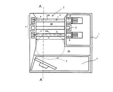
Referring to Figures 1 and 2, a coin validator body 1 defines a rectangular
cross-section coin passageway 2. The pa~sa~ w~y 2 comprises a straight,
vertical upper portion 2a, where various sensor stations 3 are located, and a
30 wider lower portion 2b. An accept gate 4 is arranged for diverting coins
along either of two routes A, B. The accept gate 4 normally blocks route A
but is opened if the signals from the sensor stations 3 inr~ t-~ that a valid coin
CA 02226617 1998-01-12
WO 97/04424 PCT/GB96
- 11 -
has been inserted into the validator. The upper portion 2a of the passageway
2 has a width ~ greater than the ~ m~ter of the largest coin 5 of interest and
a depth b greater than the thi~kn~ss of the thi~k~st coin of interest. The
entry to the upper portion 2a of the ~assag~wdy is flared so as to simplify
~lignmPnt of the validator with a coin insertion slot (not shown).
Considering the sensor stations 3 in more detail, an UPS~1C~11 optical sensor
station comprises a lensed light .omitting diode tLED) 6 mounted in the
validator body 1, so as to shine a beam U of light across the width %e~ of the
assag~wdy 2 through a slit 7 opening into the paaaagcwdy 2. The slit 7
extends across the full depth b of the upper portion 2a of the paasdg~wdy. A
lensed photosensor 8 aligned to receive the beam from the LED 6 completes
the upstream optical sensor station. A downstream optical sensor is similarly
constructed from a lensed LED 9, a slit 10 and a lensed photosensor 11 to
shine a beam D across the passdg~dy 2, and is located a short ~ t~n~e below
the upa~alll sensor. Two elongate sense coils 12 are located between the
u~a~leam and the downstream optical sensor stations. The sense coils 12 are
press fitted longit~l~in~lly into respective slots ~ ~rt.onc~ing transversely across
the width ~ of the upper portion 2a of the passag~:wdy. The sense coils 12
will be described in more. detail below.
Referring to Figure 3, the LEDS 6,9 are driven by LED driver circuitry 15 in
order to produce the upstream and downstream beams U,D. The LEDS 6~9
typically produce optical radiation in the infra-red range although visible
radiation can also be used. It will thus be appreciated that as used herein, theterm optical radiation includes both visible and non-visible optical radiation.
The photosensors 8,11 are conn~ctPc~ to interface circuitry 16 which produces
digital signals xp x2 in response to h~ellu~-;ons of the upstream and
- 30 downstream beams U,D, as a coin falls along the passageway 2 past the sensor
stations 3. The coin signals XD X2 are fed to a microprocessor 17. As
explained in our United Kingdom patent application no. 2 169 429, the
CA 022266l7 l998-0l-l2
WO 97/04424 PCT/GB96/00804
- 12 -
inductive coupling between the coils 12 and a passing coin 5 gives rise to
apparent impedance ~h~nges for the coil which are dependent on the type of
coin under test. The apparent impedance ~hanges are processed by coil
interface circuitry 18 to provide a coin parameter signals X3~ X4~ which are a
5 function of the apparent impedance rhanges
The rnicroprocessor 17 carries out a validation process on the basis of the
signals xp x2, X3~ X4 under the control of a program, stored in an EEPROM 19.
10 If, as a result of the validation processes performed by the microprocessor 17,
the coin is determined to be a true coin, a signal is applied to a gate driver
circuit 20 in order to operate the accept gate 4 CFigure 1) so as to allow the
coin to follow the accept path A. Also, the microprocessor 17 provides an
output on line 21, comprising a credit code in~irating the denominatinn of
15 the coin.
The determination of the validity of coins on the basis of signals from sense
coils is well known in the art and, accordingly, will not be described again
here in detail.
The operation of the coin rii~m-oter determining function, according to a first
embo~imPnt, will now be described with reference to Figures 4a to 4e. In this
embo~imPnt the upstream and downstream beams U,D are spaced by the
~iannrter of the coin or token to be iclentifi~cl by the validator.
Referring to Figure 4a, a coin 25, entering the passa~ w~y 2 ~;igure 1), first
intel~epL~ the upstream beam U. Unless the thirknrsc of the coin corresponds
to the depth b of the passageway 2, the beam U will not be fully blocked.
However, there will be, in any event, a signifir~nt reduction in the light
30 int~ncity detocterl by the photosensor 8 (Figure 1). Therefore, the output of the photosensor 8 is compared with a reference to determine whether the
received light im~ncity has reduced, in~irating an inCIlrSion into the upstream
CA 02226617 1998-01-12
W O 97/04424 PCT/G B96/00804
- 13 -
beam U by a coin. If an incursion is ~PtectP~, the state of signal xl rh~ng~s
This change in state is not important for coin ~ mPt~r determin~tion but may
conveniently be used as a wake up signal for the microprocessor 17 ~igure 3).
,,
5 Referring to Figure 4b, as the coin 25 continues to fall down the passageway
2, it continllPs to block the upstream beam, at least partially, and the state of
signal x, is m~int~inPc~
Referring to Figure 4c, if the coin 25 is of the desired type, it i~lL~:l.,e~s the
10 downstream beam D just as it is leaving the upstream beam U. This results in
virtually cimlllt~nPQus rh~ngPs in the states of the signals x~ and x2. In otherwords, tl = t2. In practice, t~ may not exactly equal t2 due to component
tolerances or environmPnt~i factors such as temperature. Thus, when the
microprocessor 17 (Figure 3) detects that either x, has returned to its original15 state or that x2 has rh~nge~ state to in~ir?t.o the presence of a coin, it waits to
see if the other signal makes the appropriate change of state within a
predetermined window. If the other signal makes the ~p.~p.;ate change of
state during the window, and inductive test data, derived from the coils 12
~;igure 1), is in agrppm~nt~ the microprocessor 17 (Figure 3) sends a signal to
20 the gate drive circuit 20 (Figure 3) to open the accept gate 4 ~igure 1).
Figures 4d and 4e show the coin 25 leaving the sensor stations 4.
It will be appreciated that further downstream beams could be added, spaced
25 from the upstream beam by the ~i~mPters of other coins or tokens, so that a
plurality of types of coin or token could be i~entifie~l
A second embodiment of the present invention will now be described with
reference to Figures 3, 5, 6a to 6e and 7a to 7d, wherein like parts have the
30 same reference signs as in Figures 1 and 2.
CA 022266l7 l998-0l-l2
WO 97/04424 PCT/GB96/00804
- 14-
Referring to Figure 5, the structure of the validator is s~lbst~nti llly the same as
that of Figures 1 and 2. However, the accept gate is now located in another
unit (not shown). As a result there is a larger drop between the sensor
stations 3 and the accept gate, giving more time for the validity of a coin to
5 be established. The electronic circuitry for this validator is as shown in
Figure 3. However, the EEPROM 19 will store a diLrc~c~ dnl for the
microprocessor, rPflPcring the d;Lrc~cllL validation method.
Referring to Figure 6a, a coin 25, entering the passa~,cw~Ly 2 (Figure 1), first0 hlLc~CcpLS the upstream beam U. When the incursion is c~etectecl the state ofsignal x~ rh~ngps This change in state is not important for coin ~i~m~er
determin~ri~n but may conveniently be used as a wake up signal for the
microprocessor 17.
15 Rcrc~ g to Figure 6b, as the coin continues to fall down the passagcw~y 2, it
continues to block the u~SL~ beam U, at least partially, and the state of
signal x, is ~ inf~l
Referring to Figure 6c, when the coin 25 leaves the upstream beam U, signal
20 X, returns to its original value. This change of state is noted by the
microprocessor 17 which stores a value tl, rcprpspnting the timing of the
event. Shortly thereafter, the coin i~Lc~cc~L~ the downstream beam D, causing
a change in state of signal x2. This change of state is also noted by the
microprocessor 17 which stores a value t2 repr~sPnring the timing of the event.
Referring to Figure 6d, as the coin continues to fall down the passageway 2, it
continues to block the downstream beam D, at least partially, and the state of
signal x2 is m~int~in~
30 Referring to Figure 6e, as the coin leaves the downstream beam D, the signal
x2 returns tO its original state. This change of state is noted by the
microprocessor 17 which stores a value t3 reprPsPnting the timing of the event.
CA 022266l7 l998-0l-l2
W O 97/04424 PCT/G~96,'~ r ~ ~
- 15-
Thus, after a coin has passed both beams U, D, the microprocessor 17 has
three values t" t2 and t3 from which tO derive a value int~ tive of the
~i~mPter of the coin. If it is ~cnlmP~1 that the velocity u of the coin through
the sensing beams U,D, is constant, the ~ict~n~e s travelled by a coin in a
s given time is given by the formula:
s = ut (')
Since the distance s5 between the beams is know and the time taken for the
coin to travel that ~iict~nte is known, i.e. the time between the coin leaving
the upstream beam and the coin leaving the downstream beam, the velocity of
the coin can be c~lclll~tP~I Thus, from (1):
u = S ~2)
~o Substitllting s5 for s and the measured times for t gives:
u = *
(* - tl)
Now, the upstream beam U is left when the coin has travelled a riict~n~e sO
and the downstream beam is i~ e~t~d when the coin has travelled sO + s5 -
d, where d is the ~i~mPter of the coin. Thus, from t2) and (3) above:
~ (t3 - tl)
and
sO s5 d = (t - t ) * t3 ~5)
5 Subtracting (4) from (5) gives:
* - d = ( s t ) * (t2 - t~) ~6)
CA 022266l7 l998-0l-l2
W O 97/04424 PCT/GB9G/0
- 16-
Since s5 is a constant, only
(* tl)
(t3 - tl)
need be f~ t~l in order to characterise a coin by its rli~m~t~-r.
5 Referring to Figures 7a to 7d, it can be seen that the coin 25 inLc~c~s the
downstream beam D before it clears the upstream beam U. This means that t2
is before tl. Although this produces a negative resuk when (7) is ev~ t.o~,
no problem arises because, as can be seen from (6), the negative sign merely
incli~tPs that the ~ m~ter of the coin is greater than the spacing between the
o beams. Therefore, the result of the evaluation of (7) for a large coin still
characterises the coin by its ~i~mf-t. r
A third embodiment of the present invention will now be described with
reference to Figures 8, 9, 10, lla to lle and 12a to 12h, wherein like parts
15 have the same reference signs as in Figures 1 to 7.
Referring to Figures 8 and 9, a further downstream optical sensor station,
comprising a LED 30, a slit 31 and a photosensor 32, is provided.
20 Referring to Figure 10, the electronic circuitry is s~lhst~nti~lly the same as that
of the first embo~limPnt described above, the main differences being in the
program stored in the EEPROM 19. However, the LED driving circuitry 15
is adapted to drive three LEDs 5,7,30, and the photosensor interface circuitry
16is adapted to process the signals from three photosensors 6,8,31 and output
25 an additional signal Xs.
The operation of the validator shown in Figures 8 and 9 will now be
described. However, the details of the tests relying on the coils will be
omitted as suitable techniques are well known in the art.
~=~ .
CA 022266l7 l998-0l-l2
W O 97/04424 PCT/GB96i~S~~1
-17-
Referring to Figure 11a, a coin 25, entering the passa~w~y 2 (Figure 8), first
intel~ the upstream beam U. When the incursion is ~etectec~ the state of
signal x, rhangec This change in state is not important for coin fli~mf t.or
determination but may conveniently be used as a wake up signal for the
5 microprocessor 17.
Referring to Figure 11b, as the coin 25 contin~l~os to fall down the passagt:w~y2, it continues to block the upstream beam U, at least partially, and the state
of signal x~ is m~im~inec~ until the coin 25 leaves the upsLlca m beam U, when
o signal x~ returns to its original value. This change of state is noted by the
microprocessor 17 which stores a value tl repr~s~nting the timing of the event.
Shortly thereafter, the coin i~ ep~ the first downstream bearn Dl, causing
a change in state of signal x2 . This change of state is also noted by the
microprocessor 17 which stores a value t2 l~:p~5~ ;ng the timing of the event.
Referring to Figure 11c, as the coin conrin~. s to fall down the passagt w-c.y 2,
it continues to block the first downstream bearn Dl, at least partially, and thestate of signal x2 is m~int~inP~ Next, the coin 25 inLel~L~ the second
downstream beam D2, causing a change in state of signal X5. This change of
20 state is noted by the microprocessor 17 which stores a value t3 representing
the timing of the event.
Finally, referring to Figure 11e, as the coin 25 leaves each of the downstream
beams Dl,D2, the corresponding signals X2, X5 return to their original states.
In the second embo~im~nt, described above, the speed correction is performed
on the basis of the timings of the coin 25 leaving the two bearns U,D. This
has a disadvantage in that it limits the time available, before the coin reachesthe accept gate 4, for performing the validation r~lrnl~tions. The present
30 embodiment solves this problem by means of the second downstream beam
D2 which enables the coin's speed to be determined earlier because the
e~ion of the downstream beams Dl,D2 by the leading edge of the coin
CA 022266l7 l998-0l-l2
WO 97/04424 PCT/GB96/00804
- 18-
is ~ tecter~ for this purpose. Thus, the speed of a coin can be determined
before it has past the second d~wlls~l~alll beam D2.
Now, since the speed correction is based upon the time taken for the leading
s edge of the coin to travel the ~~ict~nre s5, between the downstream beams
Dl,D2, equation (6) above becomes:
s50 - d = (* _ t) ~ (t2 - tl) or s50 f s51- d = (t - t) ~ (t3 - tl)
~8)
where *O is the ~iict~n~e between the upstream beam U and the first
downstream beam Dl.
~o
Thus, since *O and sSl are conct~ntC, a coin can be rh~r~ctPrised on the basis of
its ~i~rnpt~r by ev~hl~ting
(* - tl) or (t3 tl) (9J
(* - t2) (t3 - t2)
Referring to Figures 12a to 12h~ it can be seen that t2 occurs before tl. If thefirst form of (9) is used a negative result will be obtained. However, as with
15 the case of a large coin in a validator according to the second embo~limPnt,
the negative sign does not effect the validity of the characterisation of the coin
by its r~i~m~tf~r.
An advantage of the above-described emborlim~nts is that the beams can be
20 position such that for coin of interest, the processing means lC:CC~;Vt:S all the
tirning information within a window which is short compared with the time
required for a coin to fall through the sensor stations.
The coils 12, employed in the validators of Figures 1, 2, 5,8 and 9, will now
25 be described in detail.
CA 022266l7 l998-0l-l2
W O 97/04424 PCT/G~96~ 0
- 19-
Referring to Figure 13, a coil 12 comprises an elongate, I-section former 42
about which the winding 43 is wound. The former 42 is formed from a high
permeability material such as sintered ferrite or iron bonded in a polymer, for
example 91% ~ ice~ iron bonded in a polymer. Thus, the former 42, if it is
non-con~ cting, can serve both as a core and as a bobbin onto which the
winding 43 is wound directly.
An electromqgneti~ shield 44 comprises an elongate member having a flange
n~ing perp~n~ q-rly at each end. The shield 44 is arranged to be
o qtt~h~ d to the coil 12 such that the winding 43 is wholly covered along one
long side of the former 42 by the elongate member and at least partially
covered at the ends of the former 42. The purpose of the shield 44 is to
increase the Q of the coil 12 but also reduces both the susceptibility of the
coil 40,41 to electromqgn~tic h~L~lrt;~cnce (EMI) and the electromqgnetic
15 energy lon~qnqting from the coil, other than into the coin ~aSSdgCYVdy 2 (Figure
1) of the validator.
Referring to Figure 14, when a coil 12 is.~n~ , a mqgn~tic field 45is
projected into the coin pa~SdgCVVdy 2, between primarily the upper and lower
20 cross-pieces of the I-section former 42. A coin 25 passing along the
passagc:vvdy 2 interacts with the projected mqgnPtic field 45 varying the
apparent impedance of the coil 12.
In the foregoing embo-3imlonts of the present invention, the ~liamPnor of a coin25 is determined by the optical sensor stations as described above. At the same
time, one or more of the coils 12 are energized as set out in out our
European patent application publication no. 0 599 844. The effects of the
coin 25 interacting with the mqgnt tiC field 45 are ~l~tect~d by the coil
interface circuitry 18 which ouL~uLs signals X3, X4 to the microprocessor 17.
- 30 The microprocessor 17 then determines whether the coin under test is valid
on the basis of the signals x" x2, X5 gen~t~ by the optical sensing process
and the signals X3, X4
CA 022266l7 l998-0l-l2
W O 97/04424 PCT/GBgC/C~.~1
-20-
generated by the inductive sensing process. If the coin is valid the
microprocessor 17 sends a signal to the gate driver 20 to cause the accept gate
4 to open.
5 The microprocessor 17 carries out a validation process on the basis of the
signals xp X;?, X3, X4 under the control of a program, stored in an EEPROM 19.
If as a result of the validation processes performed by the microprocessor 17,
the coin is determined to be a true coin, a signal is applied to a gate driver
10 circuit 20 in order to operate the accept gate 4 (Figure 1) so as to allow the
coin to follow the accept path A. Also, the microprocessor 17 provides an
output on line 21, comprising a credit code in~ir~ting the denomin~tic-n of
the coin.
15 Referring to Figures 1, 5 and 8, reflective strips 100 are provided on the walls
of the passa~vv~y 2 between each of the LEDs 6,9,30 and the corresponding
photosensors 8,11,32. The reflective strips 100 increase the light im~nciry at
the photosensors 8,11,32 in the absence of a coin by rer~llring the amount of
light absorbed by the walls of the passag~w~y. As a result, the reduction in
zo light intensity at the photosensors 8,11,32, due to the passage of a coin, ismore profound than would be the case without the reflective strips 100. This
makes it easier to detect accurately the edges of passing coins.
The reflective strips 100 also solve the problem of the LEDs 6,9,30 not
25 directing light directly across the coin passageway, m lking the apparatus much
less sensitive to the orientation of the LEDs 6,9,30 and the direction in which
light is actually Pmittecl therefrom. In the ~hst-nre of the reflective strips 100,
mic~lign~c~ LEDs result in regions of the passageway 2 which are not
illnmin~t.ofl If a coin passes through one of these regions, it will not affect
30 the light in~ncity at the relevant photosensor 8,11,32.
The reflective strips 100 may be, for example, painted onto the walls of the
CA 02226617 1998-01-12
W O 97/04424 PCT/GB9GI~
- 21 -
passag~wdy 2 with mPt~llic paint or formed from metal foil stuck to the walls
of the passageway 2.
A fourth embodiment of the present invention will now be described with
reference to Figures 15 and 16, wherein like parts have the same reference
signs as in Figures 1 and 2. Since, the coils, described above with reference toFigures 13 and 14, are narrow in the direction of coin travel, it is possible tofit a plurality of them along the upper part of the coin ~assa~,cw-dy 2a.
Conceqlllqntly, it is possible to use coils, s~lbst~nti~lly as described, as sensors
for determining the rli~m~ter of a coin under test.
Referring to Figure 15, a validator is sllbstlnti~lly as described with reference
to Figure 8. However, the coils 12 and the optical sensor stations have been
replaced by three coil pairs 50,51,52, (one coil of each pair not shown) locatedat positions corresponding to those of the optical sensor stations shown in
Figure 8.
Referring to Figure 16, a coil interface circuit 18 energi~s the coil pairs
50,51,52 and p~cesses the apparent impedance rh~n~s, caused by a passing
coin, to produce six signals y~, Y2~ Y3~ Y4~ Y5~ Y6. The signals y4, y5, Y6 are
~onv~llLional coin rh~r~ct.oristic data signals and are fed to a microprocessor 17
for determin~ti~n of coin characteristic such as material and thirknrcs The
coil interface circuit 18 inrl~lcles co~ ald-urs for comparing the O~uL~ of, at
least, one coil 50,51,52 of each pair with a threshold.
As a coin passes each of the coil pairs 50,51,52, the amplitude of the respective
coil signal first falls and then rises. As these signals cross the threshold, the
ollL~ s of the respective comparators change state, producing pulse signals
which are similar to those shown in Figures 11 and 12. A ~ m~tt r value for
- 30 the coin can then be determined according to equation (9) above. However,
as the coil signals depend on the material, and som~tim~s the thirknrss of the
coin, the r~i~mPt~r value is for an apparent, or "ele~ ,",~ rtic", rli~met~r
CA 022266l7 l998-0l-l2
WO 97/04424 PCT/GB96'~
-22-
For inct~nce, a tin coin will appear to have a smaller "electrom~gnPti~
"i~mf.tor than a similarly si~d coin made from ferrom~gnt tic material.
Nevertheless, the apparent ~ m~ter determined using equation (9) above will
differ for di~rc~cll~ly sized coins of the same material.
In addition to monitoring the passage of coins into the validator, the signals
from the coil pairs 50,51,52 are cimlllt~ntoou51y used to derive additional
information about a coin under test, inrlll-ling the nature of the material of
the coin. For inct~nre~ one pair of coils may be driven in-phase and ~nother
10 in anti-phase or one coil pair could be switched between in-phase and anti-
phase configurations. Once the nature of the material is known, it is possible
to correct the '~electrom~gn~tic~ m~ter to derive the coin's physical
~i~mPt~r. However, in practice this is not n~cesc~ry because, for each coin to
be accepted, the validator could store sets of data ~1. fining values in~ir~tive of
s valid coins. The stored data would include data lcpl~ ;vc of coin
material thirknPcs, and also the "electron~gn~tic" width. Thus, it is not
n~c~sS~.y to determine the actual physical rli~m~r of a coin under test but
only the "elecL~ tic" ~ m~t~r for comparison with a value established
empirically.
A fifth embodiment of the present invention will now be described with
reference to Figures 17, 18 and 19, wherein like parts have the same reference
signs as in Figures 1,2 and 15.
Referring to Figure 17, the validator is sllhst~nti~lly the same as that shown in
Figure 15 but with the lowest coil omitted. The circuit arr~ngem~nt (Figure
18) of this embodiment is sirnilar to that shown in Figure 16. However, as
there are only two coils there are only two conventional coin rh~r~ct~ristic
30 signal lines y4 y5. Three rli~m,oter determining signal lines yp Y2~ y3 are
retained but signal y3 is derived di~crc~l-ly and the operation of the
rnicroprocessor 17 altered in consequence.
CA 022266l7 l998-0l-l2
W O 97/04424 PCT/GB~6/00~01
-23 -
The derivation of the signals y~, Y2, y3 Will now be described with reference toFigure 19. As a coin passes the upper coil 50, the amplitude of the respective
coil signal rises to a peak and then falls again. The coil interface circuit 18
compares the signal for the upper coil 50 with a first threshold ~Il and
s OuLpuLS a pulse signal y, when the coil signal is over the threshold 7~I1. The
microprocessor 17 detects the falling edge of the pulse signal Yl and stores thetime t~. As the coin passes the lower coil 51, the amplitude of the ~c~e~;vc
coil signal rises to a peak and then falls again. The coil interface circuit 18
compares the signal with both the first threshold 1~:11 and a second higher
threshold l~I2. A pulse signal Y2 is output when the coil signal is over the
first threshold 7~T1 and a pulse signal y3 when the coil signal is over the
second threshold ~2.
As described above, the time difference t2 - tl is dependent on the rii~m~ter ofa coin under test but in order to obtain a m~ningful value, a correction must
be made to take account of the velocity of the coin. In the present
emborlim~nt7 the coin's velocity is derived from the time difference t3 - t2.
This time difference depends on the peak coil signal which is in~ tive of the
material from which the coin is formed. However, the peak coil signal is
available as part of the conventional inductive testing and can be used to select
a predetermined correction factor. It should be borne in mind that correction
factors are required only where the materials and/or thi~kn~5s in~lir~t~s that
the coin may be acceptable.
Another sensor, suitable for use in place of the optical and inductive sensors
used in the foregoing embo~imt ntc, will now be described with reference to
Figures 20 and 21.
.
~eferring to Figure 20, a sensor comprises a flap 55 .o~rt.on~ing across the depth
~ 30 b of the upper part 2a of the coin passageway from the back wall thereof.
The flap 55 also extends across the full width of the upper part 2a of the coin
passageway. The flap 55 is pivotably mounted to the back wall of the coin
CA 02226617 1998-01-12
W O 97/04424 PCT/GB96/00804
-24-
passageway by a pair of spaced light leaf springs 56,57. A piezo-electric film
58 ~t~nrlc from the flap 55 to the back wall of the coin ~assdgcwdy between
the leaf springs 56,57. The film 58 may be polyvinylidene fluoride (PVDF)
sold by AMP under the trade mark Kynar~.
Referring to Figure 21, as a coin 25 travels down the coin passdgcw~y it hits
the flap 55 causing it to pivot downwardly against the leaf springs. The
pivoting of the flap 55 stresses the piezo-electric film 58 which g~n~ rat.~s anelectrical signal. This electric signal continlles to be produced as long as the10 flap 55 is displaced from its rest position. Once the coin 25 has passed the
flap 55, the leaf springs return it to its rest position, relieving the stress in the
piezo-electric film 58 and terminating the electric signal.
It will be appreciated that the duration of the electric signal produced by the
15 piezo-electric film 58 will be dependent on the coin ~liam~o~r, the speed of the
coin and the length of the flap 55, perpPnflirlllar to the back wall of the coinpassa~wdy. Consequently, the equations given above will need to be
modified to take this into account. However, since the length of the flap is
known, the n~ceSSary modifications will be readily apparent to the skilled
20 person.
A morlific~ti~n whereby the depth of the coin passa~,cwdy can be varied will
now be described with reference to Figure 22, wherein like parts have the
same reference signs as in Figures 1 and 2.
Referring to Figure 22, the t31~mPnt 60 forming the back wall of the coin
passagcwdy 2 is provided with a pair of vertical slots 61,62. One slot 61,62 is
provided on each side of the upper portion 2a of the coin passdgcwdy 2.
Since, the ~l~m~nt 60 is formed of plastics material, the back wall of the upper30 portion 2a of the passa~,cwdy 2 is able to bend to and fro about a line joining
the bottoms of the slots 61,62.
CA 02226617 1998-01-12
WO 97/04424 PCT/G~96/~E 1
- 25 -
A cam 63 is mounted behind the ~lPmPnt 60 and bears against the back wall
of the passa~;cw~y 2. The cam 63 can be rotated which causes the back wall
of the upper pa~sa~wdy portion 2a to be moved to and fro (as in~ rP~i by
the double headed arrow in Figure 22), thereby altering the depth b (as
5 in~ t~d in Figure 2) of the upper portion 2a. The bearing surface of the cam
63 is formed as a plu~lity a elongate flats so that the cam 63 will not be
turned by a force applied to the back wall of the upper passag~w~y portion
2a. In use, the cam 63 is rotated into a position which sets the depth b of the
upper passa~c:w~y portion 2a to be appropriate for the coins for which the
10 validator is ~esigne~ Thereafter, the cam 63 is not moved unless the validator
is to be used with a d;~cnt coin set. In the embodiment shown in Figure
19, the coil 12 is mounted to the moveable part of the elem.ont 60 and is
~im~onci~ned such that it does not extend beyond the slots 61,62. This means
that the coil 12 is kept as close as is possible to coins travelling through the15 passag~w~y 2 whatever the position of the cam 63.
In the in~ L~ of clarity, only the optical, inductive and piezo-electric sensors
particular to the present invention have been described. However, the skilled
person will appreciate that additional sensors and/or anti-fraud devices, of
20 which many are known in the art, could be used in addition to the sensors
described above.