Note: Descriptions are shown in the official language in which they were submitted.
CA 02227247 2001-02-16
1
BROADBAND FLAT GAIN OPTICAL AMPLIFIER
TECHNICAL FIELD:
The present invention relates to optical communications systems and
more particularly to optical systems employing optical amplifiers.
s BACKGROUND OF INVENTION:
A series of spaced-apart optical amplifiers are typically in the
transmission path of the optical communications system to amplify optical
signals
that are being transported over the path. In such systems, a plurality of
information bearing optical signals are typically transported over the optical
io path as multiplexed channels of different wavelengths. It has been noted
that if
the gain of an optical amplifier is different for the different channels being
amplified, then the difference in gain accumulates as the signal channels pass
through each of the series of amplifiers. Consequently, this results in the
channels having different signal power levels and different signal to noise
is ratios, which undoubtedly impairs the performance of the optical
communications system.
Disadvantageously, in a so-called point-to-point optical transmission
system, such differences impose a severe limitation on the number of
amplifiers that may be disposed in the transmission path before transmission
2o quality of the weak channels becomes unacceptable. Consequently, this
limits
the transmission distance in a point-to-point transmission system. Further, in
optical networks where signal channels from different transmission routes are
branched or cross-connected, such differences limit the size and scale of the
network.
CA 02227247 1998-O1-19
2
SUMMARY OF THE INVENTION:
In a lightwave communication system, the level of input power into an
optical simplifier is affected by many factors, for example, the loss between
the
signal sources and the amplifier and/or the loss between amplifiers. As such,
s the level of input power to a series of optical amplifiers in a lightwave
communiication system may be substantially different. The input power may
also vary over time as a result of changes in cable loss and aging of various
devices in the optical system. It would be advantageous that the amplifiers
maintain a flat gain spectrum for a large input dynamic range.
to W'e achieve a flat gain spectra in an optical amplifier by first amplifying
a
received optical signal and then adjusting the level of the amplified input
signal
to a predetermined level and then amplifying the adjusted signal, in which the
wavelength dependence of the optical amplifier is substantially reduced to
achieve the desired gain spectra.
is DETAILED DESCRIPTION OF THE DRAWING:
FIG. 1 illustrates an optical system in which the principles of the
invention may be practiced;
FIG. 2 is a broad block diagram of the amplifier shown in FIG. 1;
FIG. 3 is a broad block diagram of the attenuator unit of FIG. 2; and
zo FIGs. 4A through 4E respectively illustrate spectra that appear at
various points within an amplifier 100 of FIG. 2.
DETAILED DESCRIPTION:
CA 02227247 2001-02-16
3
In an illustrative example of the invention, a wavelength multiplexed
optical signal composed of a number of individual optical component signals,
e.g., N signals, having respective wavelengths of ~,,, ~,2, ~,3 .... ~,N, is
transmitted
from a source to a receiver via an optical transmission line, where N > 1 and
s may be, e.g., eight.
An illustrative optical system embodying the principles of the invention is
shown in simplified form in FIG. 1. The optical system, more particularly,
includes a plurality of laser transmitters 110-1 through 110-N, multiplexer
120,
a plurality of optical amplifiers disposed along optical transmission path
130,
io demultiplexer 140 and optical receivers 150-1 through 150- M. Each such
transmitter outputs a respective information bearing optical signal having a
unique wavelength, ~,;. It is assumed herein that such a signal is destined
for
one of the receivers 150-1 through 150-M. For the present discussion, it is
assumed that the transmission system has N optical channels respectively
is associated with transmitters 110-1 through 110-N. The N channels are
identified by their respective wavelengths, ~,,, ~.Z, ~,3 and ~,N, which are
sufficiently separated from one another to prevent signals in adjacent
channels
from interfering with one another. Such separation may be, for example, 200
GHz. The signals that are outputted by transmitters 110-1 through 110-N are
2o combined (multiplexed) at MUX 120 and then outputted to optical
transmission
line 130. The outputted signal is then transported through optical
transmission
system via amplifiers 100-1 through 100-K and optical cables 130 to DEMUX
140. DEMUX 140 separates the combined signals from one another and
supplies the separated signals to respective ones of the receivers 150-1
2s through 150-M, where M may be, for example, equal to N.
In a lightwave communication system, the input power into an optical
amplifier depends either on the loss between the signal sources and the
amplifier or on the loss between two amplifiers. As such, the input power to
CA 02227247 1998-O1-19
4
each of the optical amplifiers disposed in a lightwave communication system
may be different. The input power may also vary over time as a result of
changes in cable loss and the aging of various devices used in the system. For
these reasons an amplifier has to maintain a flat gain spectra for a large
s dynamic range of input signals.
However, the gain spectrum of an optical amplifier, which, for
Wavelength Division Multiplexed (WDM) systems and networks, typically
operate; in deep saturation, depends strongly on the input power to an optical
amplifier. What this means is that the gain spectrum of the optical amplifier
will
io vary as a function of the level of the input power. The gain spectrum of an
optical amplifier may be optimized (e.g., to decrease the dependence on the
wavelength) for one level of input signal. However, such optimization would
not
hold for differential levels of input signal, but will change accordingly.
In practical light wave communication systems, the span losses may
is vary over time and from span to span, which causes optical amplifiers on
different spans to experience large differences in "input powers". We have
recognized that it is very difficult to adjust precisely in practical systems
such
input power levels. If this is not dealt with, then the aforementioned
problems
will affect the performance, e.g.., bit error rate, of the optical system.
2o W'e have also recognized that the gain spectrum of an optical amplifier
may be adjusted for different levels of input signal power, and thus for
different
span losses. We do this, in accordance with the invention, by adjusting the
level of the input signal to a known level before the signal is amplified at a
stage of ;amplification other than the firstlinput stage. In accordance with
an
2s aspect of the invention, such adjustment is done prior to the last stage of
amplification. Moreover, such adjusting is also a function of the number of
CA 02227247 2001-02-16
channels forming the signal to be amplified, in accordance with an aspect of
the invention.
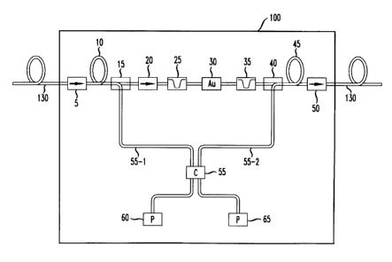
A detailed block diagram of an optical amplifier 100 is shown in FIG. 2.
Amplifier 100 , more particularly, receives a signal via optical input path
130
s and conventional optical isolator device 5. Isolator device 5 allows the
received
optical signal to propagate toward rare-earth doped fiber 10 and prevents any
spontaneous noise that is generated along the doped fiber 10 from flowing
back into input fiber 130. Doped fiber 10, which may be, for example, an
erbium
doped fiber, provides optical gain when "pumped" by optical power supplied by
io pump lasers 60 or 65 via Wavelength Division Multiplexes (WDM) 15. Pump
lasers 60 and 65 each excite the ions in doped fiber 10. The incoming signal
photons collide with the excited ions, thereby causing the ions to release
photons identical to the incoming photon. The released photons then join the
incoming photons and propagate toward isolator 20 as an amplified signal.
is Isolator 20 prevents noise and/or reflected signals traveling toward WDM 15
from interfering with the amplifier function occurring at the input stage,
i.e., the
first stage, comprising isolator 5, doped fiber 10 and WDM 15.
It is seen from FIG. 2 that coupler 55 combines the output from laser
pumps 60 and 65 and then supplies a first portion of the combined output,
i.e.,
2o pump power, to WDM 15 and supplies the remaining portion to WDM 40, in
which such portions may or may not be equal. It is noted that two laser pumps
are used in an illustrative embodiment of the invention to provide redundancy
so that amplifier 100 may continue to function properly when one of the laser
pumps is not functioning properly.
is The signal amplified by the first stage of amplifier 100 is then supplied
via conventional isolator 20 to optical filter 25 which may be designed in a
conventional way to filter out so-called Amplified Spontaneous Emission (ASE)
CA 02227247 2001-02-16
6
noise outside of the signal band of the amplified signal, and thus prevent
such
noise from competing with the amplified signal for the available power (gain)
provided at the second stage of amplifier 100. In an illustrative embodiment
of
the invention, optical filter 25 may be further designed in a conventional way
to
operate at a wavelength band lower than the lower cutoff wavelength for the
signal band, in which the latter wavelength may be, e.g., 1530 nanometers.
The filtered signal is then supplied to variable attenuator unit Au 30. A
broad block diagram of an illustrative embodiment of attenuator unit 30 is
shown in FIG. 3 and includes a conventional electrically controlled variable
io signal attenuator (hereinafter °variable attenuator") 30-5,
conventional fiber
coupler (splitter) 30-10, photo detector 30-15, optical fiber and
processor 30-25 with power table 30-20 stored in the internal memory of
processor 30-25. Specifically, coupler 30-10 supplies a predetermined portion
of the amplified signal supplied by filter 25 (FIG. 2) via variable attenuator
30-5 to photo
is detector 30-15 which outputs to processor 30-25 an electrical signal having
a
level proportional to the level of the optical signal supplied to detector 30-
15.
Processor 30-25, using the number of active channels contained in the signal
received at the input of amplifier 100 as an index, accesses a power table 30-
20 location containing a value representing the power level for the number of
2o detected channels. Processor 30-25 then converts the level of the signal
that it
receives from photo diode 30-15....... and compares that value with the value
unloaded from the accessed power table 30-20 location. If the values compare
with one another, then processor 30-25 does nothing. Otherwise, processor
30-25 sends signals to attenuator 30- 5 to adjust (increase or decrease) the
2s level of attenuation thereat until the aforementioned values compare with
one
another.
The values stored in power table 30-20 may be determined using the
following expression:
CA 02227247 2001-06-07
7
IP~~ - P N~h R ~ (e/hvs) (1 )
where IPp is the target current level; P is the target per channel power level
at the
input to fiber coupler 30-10; R is the splitting ratio of fiber coupler 30-10;
xt is the
quantum efficiency of photo detector 30-15, a is the electron charge constant
and
hvs is the energy of a signal photon. (It is noted that the photon energy is
slightly different for different channels. For the sake of simplicity, we
consider
that the level of such energy is the same or all channels.)
(It is also noted that the number of active channels may be detected by, for
example, detecting and counting so-called pilot tones respectively identifying
the
active channels in the signal received via input fiber 130.)
Returning to FIG. 2, thE; adjusted signal outputted by AU 30 is then
supplied to "gain flattening" filter 35. Filter 35, more particularly, has a
response
that is the inverse of the gain spectrum of the input and output stages of
amplifier
100 to a signal level corresponding to the level of the aforementioned
adjusted
signal, in which the output stage comprises WDM 40, doped fiber 45 and
isolator
50. The filtered signal is then supplied to WDM 40 which combines the filtered
f,0 signal and the pump power received via doped fiber 55-2 and supplies the
combined signal to doped fiber 45, whereat optical amplification of the signal
occurs in the manner discussed above. The amplified signal is then supplied to
output optical fiber 130 via isolator 50.
FIGs. 4A, 4B, 4D and 4E illustrate exemplary spectra of the signals that
respectively appear at the input of isolator 5, input of filter 35, output of
filter 35
and output of isolator 50 of amplifier 100. (note that the spectra do not
CA 02227247 2001-02-16
8
include ASE noise and are not to scale.) It is seen from those FIGs. that the
spectra is initially flat (FIG. 4A), then shaped by the input stage of
amplifier 100
(FIG. 4B), then filtered (FIG. 4D) in accordance with the loss spectrum of
filter
35 illustrated in FIG. 4C, and then amplified (FIG. 4E) by the output stage of
s amplifier 100.
The foregoing is merely illustrative of the principles of the invention.
Those skilled in the art will be able to devise numerous arrangements, which,
although not explicitly shown or described herein, nevertheless embody those
principles that are within the spirit and scope of the invention. For example,
the
Io function performed by filters 25 and 35 could be implemented by a single
filter.
Also, the amplifier could include more or less than two laser pumps. In fact,
a
single laser pump could replace the two laser pumps shown in FIG. 2.
Moreover, although the foregoing description assumed that laser pumps 60
and 65 had the same wavelengths, in alternative arrangements such
is wavelengths may be different and the coupled arrangement may be different.
For example, one laser pump could be associated solely with the first
amplifier
stage and another laser pump could be associated solely with the second
amplifier stage. Although, the foregoing description was directed to an
amplifier
having two stages, it is clear that the amplifier may include additional
stages.
2o As a further example, attenuator unit 30 may be implemented in a number of
different ways. For example, coupler 30-10 could be placed at the input to
unit
30. However, in that instance, the overall operation of attenuator unit 30
would
change to accommodate that placement.