Note: Descriptions are shown in the official language in which they were submitted.
CA 02227531 1999-07-07
1
GRAPHICS PROCESSING UNIT AND GRAPHICS PROCESSING SYSTEM
BACKGROUND
Conventionally, as described in Haruhiko Okumura, "Latest
Algorithm Dictionary in C language", p. 105 and 106, p. 162
and 163, and p. 304 published from Gijutsu Hyoronsha, Feb. 25,
1991, a method of obtaining a logarithm and an exponent by
loop calculation by performing expansion into a power series
or expansion into a continued fraction for the logarithmic
function and exponential function was used, with respect to
multiplication for obtaining XN from two digital numerical
data X and N. In accordance with this method the logarithm of
X is calculated on a software basis, and the result is
multiplied by N, and finally the exponent of the
multiplication result calculated is used.
In accordance with another method of the prior art, an
address is directly generated from the aforementioned two
digit numerical data X and N and a power table (ROM, RAM) is
used.
As mentioned above, in the conventional examples, a
problem with the speed of the process rises in the former
case, when loop ca=Lculation is generated. In the latter case,
since the two data X and N are inputted to the table, the
gradient of the input values to the table is the product of
the gradation number of X and the gradation number of N, and
the table capacity is increased.
On the other hand, as an example, a conventional graphics
processing unit, is described in Japanese Patent Application
Laid-Open 8-161525.
These conventional graphics processing units generally
comprise a geometry unit for performing geometric calculation
such as a coordinate transformation or clipping process and a
rendering unit for transforming graphics such as a straight
CA 02227531 1999-07-07
- 2
- line, a triangle, or others to pixels and performing the
drawing process.
In such a graphics processing unit, when an image
obtained by projecting various 3D graphics data is to be
generated, the geometry unit initially performs perspective
transformation of a three-dimensional shape to two-dimensional
coordinates, the clipping process, calculation of the
brightness of the light source, and others. Subsequently, the
rendering unit expands data of a straight line, a triangle, or
others of which graphics data is obtained by projection
transformation of the three-dimensional shape to two-
dimensional coordinates by the geometry unit, to pixels,
performs operations of Z comparison or alpha blending, and
stores an image in the frame memory.
In such a graphics processing unit, the geometry unit is
generally realized as a processor chip and operations of the
geometry unit are performed by handling each element of data
as a floating-point number so as to prevent limitation of the
numerical range and reduction in the operation accuracy.
On the other hand, the rendering unit is also generally
realized as a processor chip but operations thereof are
performed by handl_Lng each element of data as a fixed-point
number. The reason for this being, that it is difficult to
perform operations by the rendering unit of a floating-point
number from a viewpoint of circuit scale and operation speed.
The bit position of the decimal point of a fixed-point
number handled in t:he rendering unit generally varies with the
kind of data. The reason is that the accuracy required to
generate a good quality :image varies with the kind of data.
As mentioned above, in a conventional graphics processing
unit, the geometry unit handles data by a floating-point
number and the rendering unit handles data by a fixed-point
number, so that they number representation of data to be
handled is different between the two units. Therefore,
CA 02227531 1999-07-07
3
conventionally, th.e geometry unit transforms data after an
operation from the floating-point number to a fixed-point
number and subsequently transfers the data transformed to the
fixed-point number' to the rendering unit. For example, in the
processing unit described in Japanese Patent Application Laid-
Open 8-161525 mentioned above, by showing a number obtained by
multiplying a floating-point number by 4096 in integer
representation, the data shown in this integer representation
shows the number correctly as a fixed-point number with the
fraction part 12 bits long.
As mentioned above, in a conventional graphics processing
unit, it is necessary to transform a floating-point number to
a fixed-point number in the geometry unit. The content of
transformation to .a fixed-point number varies with the kind of
data because the bit position of the decimal point of a fixed-
point number required by the rendering unit also varies with
the kind of data.
Since the geometry unit transforms from a floating-point
number to a fixed-point number as mentioned above, the burden
of the geometry unit is increased. Since the computing element
of the geometry unit is used for transformation from a
floating-point number to a fixed-point number during this
period, the geomet=ry unit cannot perform the intrinsic process
such as coordinate transformation and the throughput of the
whole graphics processing unit is reduced. When the geometry
unit is operated b;r a program, it is necessary to define the
transformation procedure from a floating-point number to a
fixed-point number which varies with the kind of data in the
program.
SUMMARY OF THE INVENTION
An object of t:he present invention is to provide a device
for performing power calculations at high speed, by referring
to a small-capacity table, and without the requirement for
loop calculation.
CA 02227531 1999-07-07
- 4
To accomplish. this object, the present invention provides
a logarithm calculation unit for calculating and outputting a
logarithmic value of X for an input value of X by referring to
a table of logarithms, a multiplier for multiplying an output
of the logarithm calculation unit by another value of N, and
an exponent calculation unit for calculating and outputting an
exponential value for an output of the multiplier by referring
to a table of exponents. To further reduce the table capacity,
the present invention provides a logarithm shift unit for
multiplying an input of the logarithm calculation unit by 2L
for an appropriate integer L when the aforementioned input
value is not included in the input value range of the table of
logarithms.
The present invention further provides a logarithm adding
unit for setting t:he multiplication result as input of the
table of logarithms and referring to the table of logarithms
and then adding L to the referred value and setting it as
output of the logarithm calculation unit in the logarithm
calculation unit.
The present invention provides an exponent subtraction
unit for subtracting an appropriate integer M from input of
the exponent calculation unit when the aforementioned input
value is not included in the input value range of the table of
exponents and an e:cponent shift unit for setting the
subtraction result as input of the table of exponents and
referring to the table o:f exponents and then multiplying the
referred value by ~?-M and setting it as output of the exponent
calculation unit in the exponent calculation unit.
The tables of logarithms and exponents mentioned above
indicate a general circuit for calculating not only a RAM and
ROM but also a value of the logarithmic function or
exponential function for an input value within a given time.
According to t:he present invention, when a power
calculation of XN i.s to be performed for input values of X and
CA 02227531 1999-07-07
S
N, a logarithm log~aX with a base of "a" is obtained by
referring to the table of logarithms, logaXxN is calculated by
the multiplier, anal alogaXxN=XN which is the logaXxN power of
"a" is calculated by referring to the table of exponents.
Since the present invention does not perform loop calculation,
high speed calculation i.s possible. By dividing the table into
two parts such as the table of logarithms and table of
exponents, inputs of the tables can be unified to one and the
capacity of each table can be reduced.
The present invention further reduces the table capacity,
when an input value of the logarithm calculation unit is not
included in the input value range of the table of logarithms,
by multiplying the input value by 2L for an appropriate
integer L, setting the multiplication result as input of the
table of logarithms, referring to the table of logarithms, and
then adding L to t:he referred value. The present invention
then sets this val,ae as output of the logarithm calculation
unit, and when an :input value of the exponent calculation unit
is not included in the input value range of the table of
exponents, an appropriate integer M is subtracted from the
input. The present invention then sets the subtraction result
as input of the table of exponents, refers to the table of
exponents, subsequently multiplies the referred value by 2-M,
and sets it as output of the exponent calculation unit.
By doing this,, even if input values of the logarithm
calculation unit and exponent calculation unit are not
included in the input value ranges of the tables of logarithms
and exponents, power calculation can be performed. Therefore,
the input value range of the tables of logarithms and
exponents can be limited and the table capacity can be
reduced.
Another object: of the present invention is to provide a
graphics processing unit for decreasing the reduction in the
CA 02227531 2002-05-03
6
processing speed necessary to transform a floating-point
number to a fixed-point number.
To accomplish this object, the present invention
provides a graphics processing unit having a processor for
outputting graphic data including a floating-point data
string which represents information for specifying a graphic
to be drawn in the floating-point format and a rendering unit
for expanding and outputting a graphic to pixels according to
drawing data including a fixed-point data string which
represents the content of a graphic to be drawn in the fixed-
point format. The graphics processing unit further including
a data converter for converting floating-point data included
in graphic data outputted by the processor to fixed-point
data and outputting it to the rendering unit as drawing data.
The data converter also including a decimal point position
changing means for changing the bit position of the decimal
point of the fixed-point data to which floating-point data is
to be converted.
According to this graphics processing unit of the
present invention, the data converter for converting
floating-point data to fixed-point data is installed between
the processor and the rendering unit, so that the processing
of the processor and the transformation from floating-point
data to fixed-point data can be performed on a pipeline basis
and high-speed graphics processing can be performed.
Furthermore, for each floating-point data, the bit
position of the decimal point of fixed-point data to which
the floating-point data is to be converted can be changed, so
that various data can be processed.
In accordance with one aspect of the present invention
there is provided a graphics processing unit comprising: a
processor for outputting graphic data including a floating-
point data string which represents information for specifying
a graphic to be drawn in the floating point format; a
CA 02227531 2002-05-03
6a
rendering unit for expanding and outputting a graphic to
pixels according to drawing data including a fixed-point data
string which represents the content of a graphic to be drawn
in the fixed-point format, and a data converter for
converting floating-point data included in said graphic data
output by said processor to fixed-point data and outputting
it to said rendering unit as said drawing data, said data
converter having decimal point position changing means for
changing the bit position of decimal point of fixed-point
data to which floating-point data is to be converted, said
processor outputting scale factor for designating the bit
position of a decimal point of fixed-point data to which each
floating-point data is to be converted as said graphic data
together with said floating-point data string, and the
decimal point changing means of said data converter allowing
the bit position of fixed-point data to which said each
floating-point data is to be converted to set to the bit
position of a decimal point designated by said scale factor
data included in said graphic data output by said processor
for said floating-point data.
In accordance with another aspect of the present
invention there is provided a graphics processing unit
comprising: a processor for outputting graphic data including
a floating-point data string which represents information for
specifying a graphic to be drawn in the floating point
format; a rendering unit for expanding and outputting a
graphic to pixels according to drawing data including a
fixed-point data string which represents the content of a
graphic to be drawn in the fixed-point format, and a data
converter for converting floating-point data included in said
graphic data output by said processor to fixed-point data and
outputting it to said rendering unit as said drawing data,
said data converter having decimal point position changing
means for changing the bit position of decimal point of
CA 02227531 2002-05-03
6b
fixed-point data to which floating-point data is to be
converted, said processor outputting a command for indicating
the kind of a graphic specified by said floating-point data
string as said graphic data together with said floating-point
data string, said data converter having a scale factor table
for storing the bit position of decimal point of fixed-point
data to which each floating-point data included in said
graphic data is converted in correspondence with said each
command, and said decimal point changing means of said data
converter setting the bit position of a decimal point of
fixed-point data to which said each floating-point data is
converted to the bit position of a decimal point stored in
said scale factor table in correspondence with said command
included in the same graphic data as that of said floating-
point data.
BRIEF DESCRIPTION OF THE DRAWINGS
Fig. 1 is a drawing showing the circuit constitution of
a digital power arithmetic unit.
Fig. 2 is a drawing showing the operation of a logarithm
calculation unit.
CA 02227531 1999-07-07
7
Fig. 3 is a drawing showing the operation of a logarithm
shift unit.
Fig. 4 is a drawing showing the circuit constitution of a
logarithm shift unit.
Fig. 5 is a drawing showing the operation of an exponent
calculation unit.
Fig. 6 is a drawing showing the operation of an exponent
shift unit.
Fig. 7 is a drawing showing the circuit constitution of
an exponent shift unit.
Fig. 8 is a drawing showing the constitution of a
graphics system.
Fig. 9 is a drawing showing the constitution of a light
source table and a light source calculation means.
Fig. 10 is a drawing showing the constitution of a light
source table and a light source calculation means.
Fig. 11 is a block diagram showing the constitution of a
graphics processing unit.
Fig. 12 is a block diagram showing the constitution of a
computer to which a graphics processing unit is applied.
Fig. 13 is a drawing showing input and output data of the
data converter of i~he first embodiment of the present
invention.
Fig. 14 is a drawing showing the input and output data
format of the data converter of the first embodiment of the
present invention.
Fig. 15 is a block diagram showing the constitution of
the control unit of the first embodiment of the present
invention.
Fig. 16 is a block diagram showing the constitution of
the scale factor unit of the first embodiment of the present
invention.
CA 02227531 1999-07-07
8
' Fig. 17 is a block diagram showing the constitution of
the format transformation unit of the first embodiment of the
present invention.
Fig. 18 is a drawing showing input and output data of the
data converter of the second embodiment of the present
invention.
Fig. 19 is a drawing showing the input and output data
format of the data converter of the second embodiment of the
present invention.
Fig. 20 is a block diagram showing the constitution of
the control unit of the second embodiment of the present
invention.
Fig. 21 is a :block diagram showing the constitution of
the scale factor unit of the second embodiment of the present
invention.
Fig. 22 is a drawing showing input and output data of the
data converter of the third embodiment of the present
invention.
Fig. 23 is a drawing showing the format of command data
of the third embodiment of the present invention.
Fig. 24 is a block diagram showing the constitution of
the format transfo=rmation unit of the third embodiment of the
present invention.
DETAILED DESCRIPTION OF EMBODIMENTS OF THE INVENTION
Fig. 8 illust~__~ates a constitution of a graphics system
using a digital power arithmetic unit of the present
invention. The system includes a CPU 820 for executing
application software, a memory controller (MC) 830 for
controlling a main memory (MM) 840, a system bus controller
850 for controlling a system bus and a GPIF 800 for sending
data received from the system bus controller 850 to a geometry
processor 860 for performing coordinate transformation and
other processes such as FI transformation, packing, and light
source calculation, for data returned from the geometry
CA 02227531 1999-07-07
9
processor. The system aI_so includes a rendering processor 870
for expanding data sent from GPIF 800 to pixel information, a
frame memory 880 for storing pixel information generated by
the rendering processor 870, and a CRT 890 for displaying
contents of the frame processor 880.
The CPU 820 executes an application, issues a graphics
command, vertex coordinates of a graphic to be drawn, a normal
vector, texture data, reflection coefficient of materials, and
data such as color of each reflected light of the light
source, and outputs them to the GPIF 800 via the MC 830 and
the system bus controller 850. The GPIF 850 preserves the
command and data sent from the system bus controller 850 at a
GPIF input means 801.
The geometry processor 560 reads the command and data
preserved at the G:PIF input means 801, performs geometric
calculation such as coordinate transformation according to the
command and data, calculates the vertex coordinates, normal
vector, texture dai=a, and sends them to the GPIF 800.
The GPIF 800 performs FI transformation and packing, if
necessary, for the data sent from the geometry processor 860
according to the command and data, performs light source
calculation for ca=Lculating the color for each vertex, and
outputs the continuous triangle drawing command, vertex
coordinates, colors, and texture data to the rendering
processor 870.
The rendering processor 870 generates pixels inside the
graphic from the command and data by interpolation, writes the
content to be disp7_ayed on the CRT 890 into the frame memory
880 in the bit map format, and displays an image on the CRT
890.
Furthermore, the internal constitution of the GPIF 800
will be explained i.n detail.
The GPIF 800 comprises a GPIF input means 801 which is a
buffer for preserving the command and data sent from the
CA 02227531 1999-07-07
system bus controller 850, LBuf 802 which is a buffer for
preserving data sent from the geometry processor 860 for
reading a command and data and performing geometric
calculation, a BufSW register 803 for outputting a command and
5 data to a command interpretive means 806 and an FI
transformation means 804 from the LBuf 802. The GPIF 800
further comprises of a command interpretive means 806 for
interpreting a command, the FI transformation means 804 for
performing FI transformation of data, if necessary, according
10 to the command, a packing means 805 for performing the packing
process of data after FI transformation, if necessary,
according to the command, a light source table 807 for
preserving light source data necessary for light source
calculation after the FI transformation and packing process, a
light source calculation means 808 for performing light source
calculation on the basis of the light source data preserved by
the light source table 807 and calculating colors. The GPIF
800 of the present invention further comprising of a control
means 809 for controlling the order of commands and data sent
from the geometry processor 860, a packing means 805, and a
light source calcu:Lation means 808, a CBuf 810 which is a
buffer for preserv:Lng a command and data, and a BufFL register
811 for outputting a command and data to the rendering
processor 870.
Fig. 10 shows another constitution example of a graphics
system using the d_Lgital power arithmetic unit of the present
invention.
The graphics :system shown in Fig. 10 is different only in
the internal constitution of the GPIF 800 from the graphics
system shown in Fic~. 8. Accordingly, only the internal
constitution of the GPIF 800 will be explained hereinbelow in
detail.
The GPIF 800 comprises a GPIF input means 801 which is a
buffer for preserving the command and data sent from the
CA 02227531 1999-07-07
11
system bus controller 850, a LBuf 802 which is a buffer for
preserving data sent from the geometry processor 860 for
reading a command and data and performing geometric
calculation, a BufSW register 803 for outputting a command and
data to a data converter 812 from the LBuf 802, a data
converter 812 for transforming data, if necessary, from the
floating-point format to the fixed-point format according to
the command, a light source table 807 for preserving light
source data necessary for light source calculation after data
transformation, a light source calculation means 808 for
performing light source calculation on the basis of the light
source data preserved by the light source table 807 and
calculating colors. The GPIF further comprising of a control
means 809 for controlling the order of commands and data sent
from the geometry processor 860 and the light source
calculation means .908, CBuf 810 which is a buffer for
preserving a command and data, and a BufFL register 811 for
outputting a command and data to the rendering processor 870.
The light source table 807 and the light source
calculation means :308 shown in Fig. 10 are the same as the
light source table 807 and the light source calculation means
808 shown in Fig. 8. The data converter shown in Fig. 10 will
be explained in Fig. 11 and the subsequent drawings.
Fig. 9, illustrates the light source table 807 and the
light source calcu=Lation means 808, which will be described
hereinbelow in more detail.
The light source table 807 preserves parameters necessary
for light source calculation in a fixed-point number. These
parameters are div~_ded into parameters which do not depend on
the light source and parameters whose values vary depending on
the light source. The light source table 807 preserves one
parameter value inciepende~nt of the light source respectively
and 8 parameter values dependent on the light source
respectively (for 8 light: sources). When the number of light
CA 02227531 1999-07-07
12
sources is 9 or more, the values already used for calculation
are updated to new light source values sequentially one by
one.
To perform this writing control for the parameters
independent of the light source, a read pointer for indicating
which value is under calculation among the eight values at
present and a RPNT register are provided and values after the
RPNT are locked and the updating is postponed.
The light source calculation means 808 comprises an HN
inner product calculation unit 910 for calculating the inner
product of the normal vector and halfway vector, a power
calculation unit 900 for calculating the SM power of the inner
product, an LN inner product calculation unit 920 for
calculating the inner product of the normal vector and light
source vector, and a color arithmetic unit 930 for calculating
the color of each 'vertex using outputs of the power
calculation unit 900 and the LN inner product calculation unit
920.
The HN inner product calculation unit 910 calculates the
inner product of the normal vector (Nx,Ny,Nz) and the halfway
vector (Hx,Hy,Hz) and outputs the result 13 bits long to the
power calculation unit 900.
The power calculation unit 900 multiplies the output of
the HN inner product calculation unit 910 by the mirror
exponent SM (an integer from 1 to 128) of the material and
outputs the result which is 8 bits long to the color
arithmetic unit 930.
The LN inner product calculation unit 920 calculates the
inner product of the normal vector (Nx,Ny,Nz) and the light
source vector (Lx,Ly,Lz) and outputs the result to the color
arithmetic unit 930.
The color arithmetic unit 930 calculates the three colors
RGB independently, so that it has 3 sets of the same
resources. For example, with respect to R, the color
CA 02227531 1999-07-07
13
arithmetic unit 930 inputs the R component LcaR of the
environment reflected light, the R component LcdR of the
diffuse reflected light, the R component LcsR of the mirror
reflected light, the R component KaR of the environment
reflection coefficient, the R component KdR of the diffuse
reflection coefficient, the R component KsR of the mirror
reflection coefficient, the sum KR of the R components of the
radiation reflected light and the whole environment reflected
light, the product AtSp of the damping coefficient and the
spot light source effect., the output of the power calculation
unit 900, and the output of the LN inner product calculation
unit 920 and outputs the R component of the color of the
vertex, which is 8 bits long.
The constitution of the power calculation unit 900 is
shown in Fig. 1.
For the purpose of explanation, input is assumed as X or
N and output as XN. Namely, X and N correspond to the output
of the HN inner product calculation 910 and the mirror
exponent SM of the material in the above explanation. X is a
fixed-point number which is 13 bits long and the range thereof
is from 0 to 1, and N is a fixed-point number which is 8 bits
long with a range :From 0 to 128, and XN is a fixed-point
number which is 8 bits long and the range thereof is from 0 to
1.
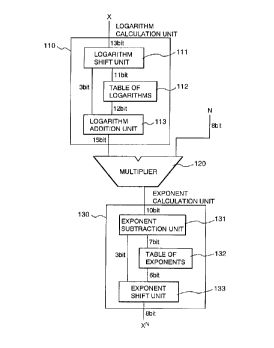
This circuit comprises a logarithm calculation unit 110
for calculating the value of the logarithmic function for
input X in a fixed--point number which is 15 bits long, a
multiplier 120 for multiplying the output of the logarithm
calculation unit 17_0 by N and outputting a fixed-point number
which is 10 bits long, and an exponent calculation unit 130
for calculating the value of the exponential function for the
output of the multiplier 120 in a fixed-point number which is
8 bits long.
CA 02227531 1999-07-07
- 14
In this case, when the logarithm calculation unit 110 and
the exponent calculation unit 130 are set as tables as they
are, in the table of logarithms, the input range is from 0 to
1 and 13 bits long and the output range is from 0 to 8
(strictly speaking, 8 is not included) and 15 bits long. In
the table of exponents, the input range is from 0 to 8
(strictly speaking, 8 is not included) and 10 bits long and
the output range is from 0 to 1 and 8 bits long and when they
are converted to memory capacity, they will be enormous
capacities such as 122880 bits and 8192 bits respectively.
However, when the tables of logarithms and exponents are
degraded, that is, the input and output ranges are limited and
the logarithm calc,alation unit 110 and the exponent
calculation unit 1:30 are structured as shown below, the
capacity of each table can be reduced extensively (24576 bits
and 768 bits when converted to memory capacity) and
calculation with the same accuracy as that before degradation
is made possible.
Namely, the logarithm calculation unit 110 comprises a
logarithm shift un_Lt 111 for shifting the input value left K
bits until it ente~__~s the input range of a degraded table of
logarithms 112 (mu=Ltiplied by 2K) and outputting a shift
amount of K, which is 3 bits long, and the shift result, which
is 11 bits long. The degraded table of logarithms 112 further
providing for outputting the value of the logarithmic function
for the shift resu7_t as a fixed-point number that is 12 bits
long. A logarithm addition unit 113 is provided for adding K
to the output of the logarithmic table 112 and outputting a
fixed-point number that is 15 bits long. The exponent
calculation unit 1..0 comprises an exponent subtraction unit
131 for subtracting M from the input value until it enters the
input range of a degraded table of exponents 132 and
outputting the subtraction amount which is 3 bits long and the
subtraction result which is also 3 bits long. The degraded
CA 02227531 1999-07-07
- 15
table of exponents 132 is provided for outputting the value of
the exponential function for the subtraction result as a
fixed-point number 6 bits long, and an exponent shift unit 133
for shifting the output of the table of exponents 132 right M
bits.
The operation when the logarith~~calculation unit. 110
calculates output Py for input Px (this operation is indicated
by the void arrow) is illustrated in Fig. 2.
The graph shown in Fig. 2 indicates a part of a
logarithmic function having a domain from 0 to 1 (strictly
speaking, 0 is not included) and a range of values from 0 to 8
(strictly speaking, 8 is not included) with a base of 2-1=0.5.
In this case, the domain means a variability domain of input
value x and the range of values means a variability domain of
output value y accompanying a variation of x.
The region 0 .indicates a portion of a domain from 0.5 to
1 (strictly speaking, 0.5 is not included) and a range of
values from 0 to 1 (strictly speaking, 1 is not included). The
table of logarithm; (12) preserves logarithmic functions
within this range. Namely, although the domain of the whole
graph is from 0 to 1, the domain within the range preserved by
the table of logar_~thms 112 is degraded to 1/2 of the domain
of the whole graph such as from 0.5 to 1. Although the range
of values of the whole graph is from 0 to 8, the range of
values within the range preserved by the table of logarithms
112 is degraded to 1/8 o:f the range of values of the whole
graph such as from 0 to 1.
The region 1 indicates a portion of a domain from 0.25 to
0.5 (strictly spea~:ing, 0.25 is not included) and a range of
values from 1 to 2 (strictly speaking, 2 is not included) and
from the property of the logarithmic function, the region 1 is
a region obtained by multiplying x by 2-1 and adding 1 to y in
the region 0.
CA 02227531 1999-07-07
16
Generally, th.e region K (K is an integer from 0 to 7)
indicates a portion of a domain from 2-K-1 to 2-K (strictly
speaking, 2-K-1 is not included) and a range of values from K to
K+1 (strictly speaking, K+1 is not included) and from the
property of the logarithmic function, the region K is a region
obtained by multiplying x by 2-K and adding K to y in the
region 0.
The logarithm shift unit 111 multiplies Px by 2K (shifted
left K) depending on which domain in the region K Px it is
included in and shifts it up to the domain in the region 0.
For simplicity, Px is assumed to be included in the
domain in the region 1 and the result of multiplying Px by 21
(1 shift) is assumed as Qx (this operation is indicated by the
arrow (1)). Qx is included in the input value range in the
table of logarithms (12), so that Qy can be obtained by
referring to the table of logarithms (12) (this operation is
indicated by the arrow (2 ) ) .
Finally, the :Logarithm addition unit 113 adds a shift
amount of 1 to Qy and calculates Py (this operation is
indicated by the arrow ( 3 ) ) .
The operation of the logarithm shift unit 111 will be
described by refer=ring to Fig. 3.
The logarithm shift unit 111 shifts the input value in
the domain in the region K left until it enters the domain in
the region 0 and outputs the shift amount and shift result at
that time.
For example, t:he domain in the region 2 is from 2-3 to 2-Z
and from 0.001000000001 to 0.010000000000 when it is indicated
in a fixed-point number of 13 bits in length. However, the
shift amount when a value of 0.001010011101 in this domain is
shifted left up to a domain from 0.100000000001 to
1.000000000000 in t:he region 0 agrees with the shift amount
when the value is ~~hifted left until 1 at the high-order.
position of 0.00101.0011100 obtained by subtracting
CA 02227531 1999-07-07
- 17
0.000000000001 from the value 0.001010011101 moves to the
second position from the high-order position. In this case,
the shift amount is 2.
The reason that 0.000000000001 is subtracted is that the
maximum value in the region such as 0.010000000000 is also
handled without exception. In this case, when the value is
shifted until 1 at the high-order position moves to the second
position from the high-order position instead of subtracting
0.000000000001, 0.100000000000 is obtained and is not included
in the domain in the region 0.
The domain in the region 0 is from 0.5 to 1 (strictly
speaking, 0.5 is not included) and is 13 bits long. However,
when the domain is set to 0 to 0.5 (strictly speaking 0.5 is
not included) by subtracting 0.5, that is, a fixed-point
number 0.100000000001 which is 13 bits long, the upper two
bits are always set to 00. By use of this, when input of the
table of logarithms 112 is set to the lower 11 bits by
removing the upper two bits which are always set to 00 from
the 13 bits of the input, 2 bits can be saved from the number
of input bits. Therefore, the value of the 11 bits obtained by
subtracting the 13 bit fixed-point number 0.100000000001 from
the shift result and removing the upper two bits is assumed as
output to the tablE=_ of logarithms 112.
The shift amount is 7 at maximum. The reason is that even
if shifted left 7 bits, a value which is not included in the
domain in the region 0 is smaller than 2-8 and will not appear
in the power result. with the accuracy of 8 bits. In such a
case, when the 13 bit fixed-point number 0.100000000001 is
subtracted, the result becomes less than 0, so that the output
value is set to 0.000000000000 by clamping 0.
In the case of. (a), the input value is 0.001001110100 and
the value obtained by subtracting 0.000000000001 is
0.001001110011. When 1 at the high-order position of the value
is shifted left 2 bits, .it moves to the second digit from the
CA 02227531 1999-07-07
- 18
high-order position, so that the shift amount is 2. Therefore,
0.100111010000 obtained by shifting the input value
0.001001110100 left 2 bits is the shift result. The output
value is 0.000111001111 obtained by subtracting 0.100000000001
from the shift result 0.100111010000.
In the case of (b), the input value is 0.000000100000 and
the value obtained by subtracting 0.000000000001 is
0.000000011111. When 1 at the high-order position of the value
is shifted left 7 bits, it moves to the second digit from the
high-order position, so that the shift amount is 7. Therefore,
1.000000000000 obtained by shifting the input value
0.000000100000 left 2 bits is the shift result. The output
value is 0.011111111111 obtained by subtracting 0.100000000001
from the shift result 0.100000000000.
In the case of (c), the input value is 0.000000000101 and
the value obtained by subtracting 0.000000000001 is
0.000000000100. Even if 1 at the high-order position of the
value is shifted lr=ft 7 bits, it will not move to the second
digit from the high-order position, so that the shift amount
is 7 at maximum. Therefore, 0.001010000000 obtained by
shifting the input value 0.000000000101 left 7 bits is the
shift result. When 0.100000000001 is subtracted from the
shift result 1.000t)00000000, the result is less than 0, so
that the output va_Lue becomes 0.000000000000 by clamping 0.
The circuit diagram of the logarithm shift unit 111 which
operates as mentioned above is shown in Fig. 4.
Since the shift amount is decided by using the value
obtained by subtracting the 13 bit fixed-point number
0.000000000001 frorn the input value as mentioned above, the
logarithm shift unlit 111 performs this subtraction immediately
after input. In the uppermost row shown in Fig. 4, the upper
8 bits of the subtraction result and input value are arranged.
The logic relating to shift is broadly divided into three
rows.
CA 02227531 1999-07-07
- 19
In the first row, NOR1 fetches NOR of the upper 5 bits
among the upper 8 bits of the subtraction result and decides
whether or not to shift the upper 8 bits of the subtraction
result and the input value left 4 bits depending on 0 or 1 of
this value.
If the output of NOR1 is 1, the upper 5 bits of the
subtraction result are all zeros and it means that there is a
space for shifting left 4 bits, so that the upper 8 bits of
the subtraction result and the input value are shifted left 4
bits. The high-order digit of the shift amount is 1. This
means that 4 bits are shifted left.
If the output of NOR1 is 0, 1 is included in the upper 5
bits of the subtra~~tion result and it means that 4 bits cannot
be shifted left, so that the upper 8 bits of the subtraction
result and the input value will not be shifted left 4 bits.
The high-order digit of the shift amount is 0. This means
that 4 bits cannot be shifted left.
Next, in the :second row, NOR2 fetches NOR of the upper 3
bits of the shift result of the subtraction result in the
first row and decides whether or not to shift the subtraction
result and the shift result of the input value in the first
row left 2 bits more depending on 0 or 1 of this value.
If the output of NOR2 is 1, the upper 3 bits of the shift
result of the subtraction result in the first row are all
zeros and it means that there is a space for shifting left 2
bits, so that the ~~ubtraction result and the shift result of
the input value in the first row are shifted left 2 bits. The
second digit of the: shift amount is 1. This means that 2 bits
are shifted left.
If the output of NOR2 is 0, 1 is included in the upper 3
bits of the shift result of the subtraction result in the
first row and it means that 2 bits cannot be shifted left, so
that the subtraction result and the shift result of the input
value in the first row will not be shifted left. The second
CA 02227531 1999-07-07
- 20
digit of the shift amount is 0. This means that 2 bits cannot
be shifted left.
Next, in the third row, NOR3 fetches NOR of the upper 2
bits of the shift result of the subtraction result in the
second row and decides whether or not to shift the subtraction
result and the shift result of the input value in the second
row left 1 bit more depending on 0 or 1 of this value.
If the output of NOR3 is 1, the upper 2 bits of the shift
result of the subtraction result in the second row are all
zeros and it means that there is a space for shifting left 1
bit, so that the subtraction result and the shift result of
the input value in the second row are shifted left 1 bit. The
low-order digit of the shift amount is 1. This means that 1
bit is shifted left.
If the output of NOR3 is 0, 1 is included in the upper 2
bits of the shift :result of the subtraction result in the
second row and it means that 1 bit cannot be shifted left, so
that the subtraction result and the shift result of the input
value in the second row will not be shifted left. The low-
order digit of the shift amount is 0. This means that 1 bit
cannot be shifted .Left.
On this stage,, the 3 bit shift amount is decided.
However, the output. value to the table of logarithms is a
value obtained by :subtracting the 13 bit fixed-point number
0.100000000001 frorn the shift result of the input value in the
third row and then clamping 0.
Next, the tab7_e of :logarithms 112 will be explained.
The input of t:he table of logarithms 112 is a fixed-point
number which is 11 bits :long in the input value range from 0
to 0.5 (strictly speaking, 0.5 is not included) as mentioned
above.
The output of the table of logarithms 112 is a value
which is obtained by indicating the value of the logarithmic
function of a value' obtained by adding the 13 bit fixed-point
CA 02227531 1999-07-07
21
. number 0.100000000001 to the input value in a fixed-point
number which is 12 bits long and the output value range is
from 0 to 1 (strictly speaking, 1 is not included). The table
of logarithms 112 may be structured so that a RAM and ROM are
incorporated and an input value is transformed to an address
and referenced. However, in this embodiment, an output
logical value is represented by a logical expression of an
input logical value and the table of logarithms 112 comprises
a circuit corresponding to the logical expression.
Assuming the :bits of input of the table of logarithms 112
as a0, al, ---, and a10 and the bits of output of the table of
logarithms 112 as b0, b1, ---, and b11, b0, b1, ---, and b11,
they can be represented by a logical expression of sum of
products of a0, al, ---, and a10. Furthermore, as a method of
setting each term of the sum of products as a main term, the
queen method and consensus method are famous. The queen
method and consensus method are described in Munehiro Goto,
"Computer Engineering for Electric and Electronic Students",
p. 40 to 45 published by Maruzen Co., Ltd., June 30, 1983.
It is possiblE: to constitute the table of logarithms 112
by a circuit corre:~ponding to a logical expression generated
by one of the aforementioned methods.
As a result of actual logical composition, a 0.35-~m CMOS
requires an about-~6k gate.
Finally, the :Logarithm &addition unit 113 will be
explained.
The input of t:he logarithm addition unit 113 is shift
amount calculated by the logarithm shift unit 111 and the
output of the table of logarithms 112.
The logarithm addition unit 113 adds and outputs this
shift amount to the output value of the table of logarithms
112.
The output value range of the table is from 0 to 1
(strictly speaking, 1 is not included) and the shift amount is
CA 02227531 1999-07-07
- 22
- an integer, so that the output of the logarithm addition unit
113 is a fixed-point number which is 15 bits long, which are
obtained by adding 3 bits of the shift amount to the high-
order position of 12 bits of the output value of the table.
Next, the multiplier 120 will be explained.
The input of the multiplier 120 is an output of the
logarithm calculation unit 110 and N.
The multiplier 120 multiplies the 15 bit output of the
logarithm calculation unit 110 by N 8 bits long and outputs
the product as a fixed-point number of 10 bits in length in
the output value range from 0 to 8 (strictly speaking, 8 is
not included) .
When the multiplication result is 8 or more, it is
clamped to the maximum output value. The reason is that the
power of 8 or more of 2-'~ is smaller than 2-8 and will not
appear in the power result with the accuracy of 8 bits.
The operation when the exponent calculation unit 130
calculates output 1?y for input Px (this operation is indicated
by the void arrow) by referring to Fig. 5.
The graph shown in Fig. 5 indicates a part of an
exponential function having a domain from 0 to 8 (strictly
speaking, 8 is not included) and a range of values from 0 to 1
(strictly speaking,, 0 is not included) with a base of 2-1=0.5.
The region 0 .indicates a portion of a domain from 0 to 1
(strictly speaking,, 1 is not included) and a range of values
from 0.5 to 1 (strictly speaking, 0.5 is not included) and the
table of exponents 132 preserves exponential functions within
this range. Namely,. although the domain of the whole graph is
from 0 to 8, the domain within the range preserved by the
table of exponents 132 is degraded to 1/8 of the domain of the
whole graph such a:~ from 0 to 1 and although the range of
values of the whole graph is from 0 to 1, the range of values
within the range preserved by the table of exponents 132 is
degraded to 1/2 of the range of values of the whole graph such
CA 02227531 1999-07-07
. 23
as from 0.5 to 1. The region 1 indicates a portion of a domain
from 1 to 2 (strictly speaking, 2 is not included) and a range
of values from 0.25 to 0.5 (strictly speaking, 0.25 is not
included) and from the property of the exponential function,
the region 1 is a region obtained by adding 1 to x and
multiplying y by 2-1 in the region 0.
Generally, the region M (M is an integer from 0 to 7)
indicates a portion of a domain from M to M+1 (strictly
speaking, M+1 is not included) and a range of values from 2-M-1
to 2-M (strictly peaking, 2-M-1 is not included) and from the
property of the exponential function, the region M is a region
obtained by adding M to x and multiplying y by 2-M in the
region 0.
The exponent subtraction unit 131 subtracts M from Px
depending on which domain in the region M Px is included in
and slides it up to the domain in the region 0.
For simplicity, Px is assumed to be included in the
domain in the region 1 and the result of subtracting 1 from Px
is assumed as Qx (t=his operation is indicated by the arrow
(1)). Qx is included in the input value range in the table of
exponents 132, so l.hat Qy can be obtained by referring to the
table of exponents 132 (this operation is indicated by the
arrow ( 2 ) ) .
Finally, the E=xponent shift unit 133 shifts Qy right 1 of
the subtraction amount (2-1 is multiplied) and calculates Py
(this operation is indicated by the arrow (3)).
The logarithm subtraction unit will be explained.
The input of t=he logarithm subtraction unit 131 is a 10
bit fixed-point number in the input value range from 0 to 8
(strictly speaking, 8 is not included). As mentioned above,
the exponent subtraction unit 131 subtracts M from Px
depending on which domain in the region M the value is
included in and slides ii. up to the domain in the region 0.
However, M is the upper 3 bits of the input value and a value
CA 02227531 1999-07-07
24
obtained by subtracting M from the input value is the lower 7
bits of the input value.
Next, the table of exponents 132 will be explained.
The input of the table of exponents 132 is an output of
the exponent subtraction unit 131 and is a fixed-point number
which is 7 bits long in the input value range from 0 to 1
(strictly speaking, 1 is not included).
The range of values in the region 0 is from 0.5 to 1
(strictly speaking, 0.5 is not included). However, when the
range of values is moved in parallel by -0.5 in the y
direction so as to obtain a range of values from 0 to 0.5
(strictly speaking, 0.5 is not included), the upper 2 bits of
the output of the table of exponents 132 become 00 and the
number of output bats can be reduced by 2 bits.
Therefore, the output of the table of exponents 132 is a
6 bit fixed-point number obtained by subtracting 0.5, that is,
the 8 bit fixed-point number 0.1000001 from the value of the
exponential function of the input value which is indicated by
a fixed-point number which is 8 bits long and the output range
at this time is from 0 to 0.5 (strictly speaking, 0.5 is not
included) .
The table of exponents 132 also may be structured so that
a RAM and ROM are -Lncorporated and an input value is
transformed to an address and referred to. However, in this
embodiment, an output logical value is represented by a
logical expression of an input logical value and the table of
exponents 132 comprises a circuit corresponding to the logical
expression.
As a result of: actual logical composition, a 0.35-~m CMOS
requires an about-l.k gate.
Finally, the c>perat:ion of the exponent shift unit 133
will be explained by referring to Fig. 6.
CA 02227531 1999-07-07
The input of the exponent shift unit 133 is the
subtraction number which is an output of the subtraction unit
and the output of the table of exponents 132.
As mentioned above, since the output of the table of
5 exponents 132 is a 6 bit fixed-point number obtained by
subtracting 0.5, that is, the 8 bit fixed-point number
0.1000001 from the value of the exponential function of the
input value which is indicated by a fixed-poirit number which
is 8 bits long, it is necessary that the exponent shift unit
10 133 inversely adds 0.5, that is, the 8 bit fixed-point number
0.1000001 to the output of the table of exponents 132 and
returns the range of values to 0.5 to 1 (strictly speaking,
0.5 is not included). Next, the exponent shift unit 133 shifts
and outputs the va=Lue right of the subtraction amount.
15 In the case o:E (a), when the 8 bit fixed-point number
0.1000001 is added to the output 0.01011 of the table of
exponents 132 and it is shifted right 2 of the subtraction
amount, an output value of 0.0010011 is obtained. Zeros are
put in the upper b_Lts which become empty due to right
20 shifting.
In the case of (b), when the 8 bit fixed-point number
0.1000001 is added to the output 1.01101 of the table of
exponents 132 and ~_t is shifted right 5 of the subtraction
amount, an output value of 0.0000011 is obtained.
25 The circuit diagram of the exponent shift unit 133 which
operates as mentioned above is shown in Fig. 7.
The input of t:he exponent shift unit is the 3 bit
subtraction amount which is an output from the exponent
subtraction unit and the output which is 6 bits long from the
table of exponents 132. To the output from the table of
exponents 132, the 8 bit fixed-point number 0.1000001 is added
immediately after input. The addition result is a fixed-point
number which is 8 f>its long.
CA 02227531 1999-07-07
26
The logic relating to the shift is broadly divided into
three rows.
In the first row, when the low-order digit of the
subtraction number is 1, the addition result is shifted right
one bit position and when the low-order digit of the
subtraction number is 0, the addition result is not shifted
right.
Next, in the second row, when the second digit of the
subtraction number is 1, the shift result of the addition
result in the first row is shifted right 2 bits. When the
second digit of the subtraction number is 0, the shift result
of the addition result in the first row is not shifted right.
Finally, in t:he third row, when the high-order digit of
the subtraction number is 1, the shift result of the addition
result in the second row is shifted right 4 bits. When the
high-order digit o:f the subtraction number is 0, the shift
result of the addition result in the second row is not shifted
right.
In this embodiment, when all the multiplication units are
mounted in a 0.35-~m CMOS, an about-7.5k gate is required and
the operation is completed within about 35 ns. By doing this,
light source calcu:Lation can be embedded in the GPIF 800 chip
and the processing of the geometry processor 860 can be
reduced, so that the performance of the system can be improved
about 2 times.
Since the dig_Ltal power arithmetic unit of the present
invention performs operations by referring to the tables as
mentioned above, the operation result can be obtained more
rapidly than loop calculation.
By dividing the table into two parts such as the table of
logarithms and table of exponents, inputs of the tables can be
unified to one and the capacity of each table can be reduced.
The capacity of the table of logarithms can be further
reduced by multiplying, the input value by 2L for an
CA 02227531 1999-07-07
27
appropriate integer L, when an input value of the logarithm
calculation unit is not included in the input value range of
the table of logarithms, setting the multiplication result as
input of the table of logarithms, referring to the table of
logarithms, and then adding L to the referred value. The
capacity of the table of exponents can be further reduced by
subtracting, when an input value of the exponent calculation
unit is not included in the input value range of the table of
exponents, an appropriate integer M from the input value, and
setting the subtraction result as input of the table of
exponents, referring to the table of exponents, and then
multiplying the referred value by 2-M.
Fig. 11 shows the constitution of a graphics processing
unit. As shown in the drawing, the graphics processing unit
comprises a geometry processor 1105, a data converter 1110, a
rendering processor 1150, and a frame memory 1160.
The data converter 1110 comprises a controller 1140, a
scale factor unit :L130, and a format transformation unit 1120.
The constitution of a graphics processing system to which
the graphics proce:~sing unit shown in Fig. 11 is applied is
shown in Fig. 12.
As shown in the drawing, in this system, a CPU 1216, a
memory 1211, an external storage 1212, and an input unit such
as a keyboard, mou:~e, and pen input tablet are connected via a
bus 1214. On the bus 1214, a slot 1215 for loading an extended
card is provided and graphics processing unit 1200 is realized
as an extended card which is connected to the bus 1214 via
slot 1215. To the graphics processing unit 1200, a CRT 1270
which is a display unit :is connected.
In this const~_tution, the CPU 1216 executes an
application read from the memory 1211, generates graphics data
comprising vertex coordinates, normal vector, and texture
given by a graphic: command such as a triangle or straight
CA 02227531 1999-07-07
28
line and a floating-point number, and gives it to the geometry
processor 1105 via. the system bus.
The geometry processor 1105 performs coordinate
transformation, the clipping process, and calculation of the
brightness of the light source for the graphics data,
transforms a command such as a triangle or straight line and
coordinates and brightness data after the geometry process to
graphic data comprising a scale factor and floating-point data
string, and outputs it to the data transformation unit 1110.
The data transformation unit 1110 transfers drawing data
which is obtained by converting the graphic data transferred
from the geometry processor 1105 to a fixed-point data string
to the rendering processor 1150.
The rendering processor 1150 expands data of a straight
line or triangle indicated by the drawing data which is
obtained by converting graphic data to a fixed-point number by
the data transformation unit 1110 to pixels, performs
operations such as Z comparison between the rendering
processor 1150 and the frame memory 1160 and alpha blending,
and performs a progress of storing pixels obtained as an
operation result in the frame memory 1160.
The frame memory 1160 is always read and the contents of
the frame memory 1:160 are displayed on the CRT 1270 which is a
display unit.
The graphics processing unit 1200 can be applied to
various devices not. only the device shown in Fig. 2 but also
game devices and computers and word processors having a
constitution other than the one shown in Fig. 2.
With respect t:o details of the graphics processing unit,
the data converter 1110 which is a most characteristic part of
the present invent_Lon wi:l1 be mainly explained. This data
converter 1110 can be applied also to the data converter 812
shown in Fig. 10. Firstly, graphic data inputted to the data
converter 1110 from the geometry processor 1105 and drawing
CA 02227531 1999-07-07
29
data outputted to the rendering processor 1150 from the data
converter 1110 will be explained.
As shown in Fig. 13, graphic data given to the data
converter 1110 from the geometry processor 1105 comprises a
command code, scale data, and floating-point data 1 to 8.
For example, in graphic data of a straight line, a
drawing command of a straight line, a transfer number 7, and
an address are inputted into the command code field, and a
scale factor to be used to convert floating-point data 1 to 7
to fixed-point data 1 to 7 is inputted into the scale data
field. The X coordinate of the start point of floating-point
data is inputted into the floating-point data 1 field, and the
Y coordinate of the start point of floating-point data is
inputted into the :floating-point data 2 field. The X
coordinate of the end point of floating-point data is inputted
into the floating-point data 3 field, and the Y coordinate of
the end point of f:Loating-point data is inputted into the
floating-point data 4 field. The brightness R of floating-
point data is input=ted into the floating-point data 5 field,
and the brightness G of floating-point data is inputted into
the floating-point data 6 field, while the brightness B of
floating-point data is inputted into the floating-point data 7
field.
As shown in F_Lg. 13, the data converter 1110 receives
such graphic data and transfers the command code and the
fixed-point data 1 to 8 which convert the floating-point data
1 to 8 to fixed-point data to the rendering processor 1150 as
drawing data.
For example, in drawing data converted from the
aforementioned graphic data of a straight line, a drawing
command of a straight line, a transfer number 7, and an
address are inputtE:d into the command code field. The X
coordinate of the start point of fixed-point data is inputted
into the fixed-point data 1 field, and the Y coordinate of the
CA 02227531 1999-07-07
start point of fixed-point data is inputted into the fixed-
point data 2 field. The X coordinate of the end point of
fixed-point data is inputted into the fixed-point data 3
field, and the Y coordinate of the end point of fixed-point
5 data is inputted into the fixed-point data 4 field. The
brightness R of fixed-point data is inputted into the fixed-
point data 5 field, and the brightness G of fixed-point data
is inputted into t:he fixed-point data 6 field, while the
brightness B of fi:Ked-point data is inputted into the fixed-
10 point data 7 field.
The format of input and output data of the data converter
1110 mentioned abo~se is shown in Fig. 14.
The command code comprises an operation code, other
control codes, a t=ransfer number, and an address. In the
15 operation code field, the operation content to be instructed
to the rendering processor 1150 is written, and in the
transfer number field, the number of data of the fixed-point
number to be transferred to the rendering processor 1150 is
written. In the address field, the register of the rendering
20 processor 1150 which is a writing destination of graphic data
is written. In the' other control codes field, control
information to be notified to the rendering processor 1150 or
the data converter 1110 from the geometry processor 1105 is
stored as required..
25 Next, the sca7_e data includes Scalel to Scale8 and a
scale factor is written in each scale field. Scalel
corresponds to the floating-point data 1 and the fixed-point
data 1 shown in Fic~. 13. Scale2 corresponds to the floating-
point data 2 and the fixed-point data 2 and the same may be
30 said with Scale3 to Scale8. In this case, for example, when
the value of Scalel. is 3, it indicates that the position of
the decimal point of the fixed-point data 1 to be transferred
to the rendering processor 1150 from the data converter 1110
is at the third bit. from the low-order position and when the
CA 02227531 1999-07-07
31
value of Scale2 is 5, it indicates that the position of the
decimal point of the fixed-point data 2 to be transferred to
the rendering processor 1150 from the data converter 1110 is
at the fifth bit from the low-order position.
Next, the floating-point data comprises a code 1 bit
long, an exponent 8 bits long, and a mantissa 23 bits long in
the known single floating-point representation of IEEE.
Finally, the fixed-point data comprises a code, an
integer part, and .a fraction part and the bit position of
decimal point varies with the scale factor.
The operation of the data converter 1110 will be
explained hereunde:r.
In the data converter 1110, the controller 1140 gives an
instruction for setting scale factors and deciding a scale
factor to be used ao as to decode the command code of graphic
data comprising a command code, scale data, and floating-point
data generated by i:he geometry processor 1105 and to convert
the floating-point data to fixed-point data.
The scale factor unit 1130 operates according to a
control signal for issuing an instruction to set a scale
factor string and t:o use which scale factor from the
controller 1140 anti gives the scale factor, that is, the bit
position of the decimal point of the fixed-point number to the
format transformation unit 1120.
The format transformation unit 1120 converts the
floating-point data from the geometry processor 1105 to fixed-
point data so as to correspond to the scale factor received
from the scale factor unit 1130 and gives it to the rendering
processor 1105.
Each unit will. be explained in detail hereunder.
Fig. 15 shows the constitution of the controller 1140.
The controller 1140 comprises a sequencer 1141 for
controlling the status of the data converter 1110 and
controlling transfer of graphic and drawing data for the
CA 02227531 1999-07-07
32
. geometry processor 1050 and the rendering processor 1150, a
counter circuit 1142 for controlling the number of data of
fixed-point number to be transferred to the rendering
processor 1150, and a LEN register 1143 for storing the
transfer number included in the command code.
The statuses controlled by the sequencer 1141 are the
status that the data converter 1110 receives the command code
from the geometry :processor 1105, the status that it receives
scale data, and the status that it receives the floating-point
data 1 to 8.
In the status that the command code is received, the
sequencer 1141 outputs an instruction for setting the transfer
number in the comm;~nd code to the LEN register 1143, outputs
an instruction for initializing the CNT register indicating
the number of fixed-point data transferred to the rendering
processor 1150 to t=he counter circuit 1142, outputs a command
code writing reque:~t DC_W signal among the drawing data to the
rendering processorr 1150, and transfers the command code to
the rendering processor 1150. When an RP ACC signal indicating
that the drawing data command code is received from the
rendering processor 1150 is returned, the sequencer 1141
outputs a DC ACC signal indicating that the command code is
received to the geometry processor 1105 and moves the status
to the status that the scale data is received.
Next, in the ;status that the scale data is received, the
sequencer 1141 outputs an instruction SET signal for writing
scale data to the :kale :factor unit 1130, outputs a DC ACC
signal indicating that the scale data is received to the
geometry processor 1105, and moves the status to the status
that the floating-point data 1 to 8 are received.
Next, in the ~~tatus that the floating-point data 1 to 8
are received, the ~~equencer 1141 outputs a fixed-point data
writing request DC_W signal to the rendering processor 1150
and when an RP ACC signal indicating that the fixed-point data
CA 02227531 1999-07-07
33
is received from the rendering processor 1150 is returned, the
sequencer 1141 outputs a DC ACC indicating that the graphic
data is received to the geometry processor 1105.
Furthermore, in the status that the floating-point data 1
to 8 are received, when the sequencer 1141 receives an
instruction for returning the status to the status that the
command code is received from the counter circuit 1142, the
sequencer 1141 moves the status to the status that the command
code is received. When the command code is not received, the
sequencer 1141 repeats the aforementioned operation in the
status that the floating-point data 1 to 8 are received.
The counter circuit 1142 outputs an instruction for
returning to the status that the command code is received as
mentioned below.
As mentioned above, the LEN register 1143 is a register
for storing the tr<~nsfer number in the command code and stores
it according to the instruction for setting the transfer
number in the comm<~nd code from the sequencer 1141 and outputs
the stored value to the counter circuit 1142. The counter
circuit 1142 comprises a CNT register and a comparator. The
CNT register initializes the register value to 0 when it
receives an initia:Lization instruction from the sequencer 1141
and gives the value of t:he CNT register to the scale factor
unit 1130. When an RP ACC signal indicating that the fixed-
point data of drawing data is received from the rendering
processor 1150 is ~:eturned in the status that the sequencer
1141 receives the i=loating-point data 1 to 8, the sequencer
1141 increments the' value of the CNT register. The comparator
compares the incremented value of the CNT register and the
value of the LEN register. When the value of the CNT register
and the value of the LEN register agree with each other, the
comparator gives an instruction for returning to the status
that the command code is received to the sequencer 1141.
CA 02227531 1999-07-07
34
. Next, the constitution of the scale factor unit 1130 is
shown in Fig. 16.
As shown in the drawing, the scale factor unit 1130
comprises registers S1 1611, S2 1612, S3 1613, S4 1614, S5
1615, S6 1616, S7 1617, and S8 1618 and a selector.
The registers S1 1611 to S8 1618 are registers preserving
a scale factor corresponding to each of the floating-point
data 1 to 8 and when a writing instruction SET signal is
received from the ~~ontroller 1140, the registers divide and
write 32-bit scale data transferred from the geometry
processor 1105 into 4 bits each.
The selector :1620 selects one of the values of the
registers S1 1611 ~~o S8 1618 according to a counter value CNT
signal inputted from the controller 1140 and outputs it to the
format transformation unit 1120. By doing this, a scale factor
corresponding to each of the floating-point data 1 to 8 of
graphic data can bE~ given to the format transformation unit
1120.
Next, the con:~titution of the format transformation unit
1120 is shown in Fig. 17.
As shown in the drawing, the format transformation unit
1120 comprises an exponent processing unit 1710 for obtaining
a shift amount frorn the scale factor and the exponent of a
floating-point number, a mantissa shift unit 1730 for shifting
the mantissa of a f=loating-point number right and converting
it to a positive fixed-point number, and a sign processing
unit 1750 for converting the positive fixed-point number
obtained by the mantissa shift unit to a negative fixed-point
number when the sign of the floating-point number is negative.
The exponent processing unit 1710 adds the value of the
scale factor outputted from the scale factor unit 1130 to the
exponent of the flc>ating--point number, performs offset
correction by subtracting an offset value of 127 from the
addition result, performs bit inversion by pulling out only
CA 02227531 1999-07-07
the lower 5 bits, and then obtains the shift amount of the
mantissa shift unit 1730.
The reason that an offset value of 127 is subtracted from
the addition result is that an offset value of 127 is added to
5 the exponent of this floating-point number in the IEEE
standard. The reason that only the lower 5 bits are pulled
out is that the shaft amount requires only 5-bit information
so as to convert to a 32-bit fixed-point number. The reason
that bit inversion is performed is that although the value of
10 the exponent is to be shifted left, it is transformed to a
right shift.
When a value obtained by adding the value of the scale
factor outputted f~__~om the scale factor unit 1130 to the
exponent of the floating-point number is less than a constant
15 of 127, even if an attempt is made to convert to a 32-bit
fixed-point number,. the value is too small to be represented,
so that the exponent processing unit 1710 also performs a
process of outputting an instruction for clamping the data of
fixed-point number to 0 to the sign processing unit 1750.
20 Next, the mantissa shift unit 1730 puts 1 in the most
significant bit, puts a 23-bit mantissa of the floating-point
number in bits 30 t:o 8, obtains a 32-bit coefficient when bits
7 to 0 are set to C~, shi:Ets the 32-bit coefficient right the
shift amount obtained by the exponent processing unit 1710,
25 and converts it to a positive fixed-point number. The reason
that 1 is put in the most significant bit of the 32-bit
coefficient is that: 1 at the most significant position of the
mantissa is omitted in the IEEE standard.
Next, when they sign of the floating-point number is
30 negative, the sign processing unit 1750 converts the positive
fixed-point data obtained by the mantissa shift unit 1730 to
negative fixed-point data and furthermore when clamping is
instructed from the:
CA 02227531 1999-07-07
36
. exponent processing unit 1710, the sign processing unit 1750
sets the fixed-point data to 0 and transfers the fixed-point
data to the rendering processor 1150.
Next, an example that a floating-point number of 2.625 is
converted to a fix~=_d-point number with the fraction part 3
bits long will be chown.
In the floating-point number 2.625, the sign bit is
represented by (0)>, and the exponent by (10000000)2, and the
mantissa by (01110000000000000000000)2.
When the exponent processing unit 1710 adds the bit
position of the decimal point and the exponent, (10000011)2 is
obtained and when :it performs offset correction by subtracting
127, (00000100)2 i~; obtained.
Then, when the. lower 5 bits are pulled out, (00100)2 is
obtained, and when bit inversion is performed, (11011)2 is
obtained, and the ;shift amount becomes 27.
The 32-bit coefficient of the mantissa shift unit 1730
becomes (10101000000000000000000000000000)2, and when it is
shifted right 27 b_Lts, it becomes
(00000000000000000000000000010101)2, and a positive fixed-point
number can be obta~_ned.
The part more than :3 bits from the low-order position
which is an integer part indicates 2 and the part of the lower
3 bits which is a fraction part indicates 0.625.
In the sign px-ocess:ing unit 1750, the sign bit (0)2
indicates positive, so that a positive fixed-point number is
not converted to a negative fixed-point number and transferred
to the rendering processor 1150.
The first embodiment of the graphics processing unit has
been explained above.
Next, the second embodiment of the graphics processing
unit will be explained.
CA 02227531 1999-07-07
37
The whole constitution of the graphics processing unit of
the second embodiment is the same as the constitution shown in
Fig. 11 and can be applied to the system shown in Fig. 12.
Fig. 18 shows graphic data inputted to the data converter
1110 from the geometry processor 1105 and drawing data
outputted to the rendering processor 1150 from the data
converter 1110 in 'the second embodiment.
As shown in t:he drawing, the graphic data in the second
embodiment is graphic data when the scale data is omitted from
the graphic data inputted to the data converter 1110 from the
geometry processor 1105 in the first embodiment.
Next, the format of input and output data of the data
converter 1110 is chown in Fig. 19.
As shown in F:ig. 19, the formats of the floating-point
data, fixed-point data, and command data are the same as those
explained in the first embodiment.
The constitution of graphic data outputted from the
geometry processor 1105 can be specified from the operation
code of the command code.
For example, when the operation code is (0001)2, it means
a command for draw_Lng a straight line and in this case, it is
decided that the f_Loating-point data 1 to 7 indicate the X and
Y coordinates of the start point, the X and Y coordinates of
the end point, and the brightnesses R, G, and B. On the other
hand, when the operation code is (0010)2, it means a command
for drawing a triangle and it is decided that the floating-
point data 1 to 5 indicate the X and Y coordinates of the
vertex and the bridhtnesses R, G, and B. When one triangle is
to be displayed on the CRT 700, the graphic data of the
triangle is given t:o the rendering processor 500 three times.
As mentioned ~~bove, for the value of the operation code,
the kind of each f7_oating-point data following the command
code including the operation code is decided. Therefore, in
the second embodiment, by deciding the bit position of the
CA 02227531 1999-07-07
38
decimal point of the fixed-point data to which the floating-
point data is converted according to the preset correspondence
depending on the operand. code and the position of floating-
point data so that, for example, when the operation code is
(0001)2, the data <:onverter 1110 converts the X coordinate of
the start point of the floating-point data 1 to the fixed-
point data 1 whose decimal point is located at the third bit
from the low-order position and converts the Y coordinate of
the start point of the floating-point data 2 to the fixed-
point data 2 whose decimal point is located at the second bit
from the low-order position. When the operation code is
(0010)2, the data converter 1110 converts the X coordinate of
the vertex of the :Floating-point data 1 to the fixed-point
data 1 whose decimal point is located at the fourth bit from
the low-order posil~ion and converts the Y coordinate of the
vertex of the floai~ing-point data 2 to the fixed-point data 2
whose decimal poinl~ is located at the second bit from the low-
order position. Each floating-point data is converted to a
fixed-point number having the bit position of the decimal
point according to the data kind without receiving the scale
data from the geometry processor 1105 like the first
embodiment.
The data converter 1110 for performing such a conversion
will be explained _Ln detail hereunder. The whole constitution
of the data converter 11:10 is the same as that shown in Fig.
11 and the data converter 1110 comprises the controller 1140,
the scale factor unit 11:30, and the format transformation unit
1120.
Fig. 20 shows the constitution of the controller 1140.
As shown in the drawing, the controller 1140 comprises a
sequencer 2015 for controlling the status of the data
converter 1110 and controlling the transfer of graphic and
drawing data for tree geometry processor 1050 and the rendering
processor 1150, a counter circuit 2020 for controlling the
CA 02227531 1999-07-07
39
number of data of fixed-point number to be transferred to the
rendering processor 1150, and a transfer number look-up table
2035 for detecting the transfer number in the command code
from the operation code.
The statures ~~ontrolled by the sequences 2015 are the
status that the data converter receives the command code from
the geometry processor 1105 and the status that it receives
the floating-point data 1 to 8.
In the status that the command code is received, the
sequences 2015 stores the operation code of the command code
in the COM register, outputs the content of the operation code
to the transfer number look-up table 2035, outputs an
instruction for initializing the CNT register to the counter
circuit 2020, outputs a drawing data command code writing
request DC W signa_L to the rendering processor 1150, and
transfers the command code to the rendering processor 1150.
When an RP ACC signal indicating that the drawing data command
code is received from the rendering processor 1150 is
returned, the sequences 1141 outputs a DC ACC signal
indicating that the graphic data is received to the geometry
processor 1105 and moves the status to the status that the
floating-point data 1 to 8 are received.
Next, in the :status that the floating-point data 1 to 8
are received, the :~equencer 2015 gives the value of the COM
register storing tree operation code to the scale factor unit
1130, outputs a fi~;ed-point data writing request DC W signal
to the rendering processor 1150, and when an RP ACC signal
indicating that the' fixed-point data is received from the
rendering processor 1150 is returned, the sequences 2015
outputs a DC ACC signal indicating that the floating-point
data is received to the geometry processor 1105. Furthermore,
in the status that the floating-point data 1 to 8 are
received, when the sequences 2015 receives an instruction for
returning the status to the status that the command code is
CA 02227531 1999-07-07
received from the counter circuit 2020, the sequencer 2015
moves the status to the status that the command code is
received. When the command code is not received, the sequencer
2015 repeats the aforementioned operation in the status that
5 the floating-point data 1 to 8 are received.
The transfer :number look-up table 2035 registers the
values of transfer numbers of fixed-point data L1 to L16 for
each operation code, selects one value from them according to
the value of the COM register outputted from the sequencer
10 2015 by a selector 2036, and gives it to the counter circuit
2020.
For example, when a transfer number of 7 is registered in
L1 and a transfer number of 5 is registered in L2 and the
value of the COM rE~gister, that is, the operation code is
15 (0001)2, the transfer number 7 is given to the counter circuit
2020 and when the value of the COM register is (0010)2, the
transfer number 5 :is given.
The counter c:~rcuit 2020 comprises a CNT register and a
comparator. The CNT register initializes the register value
20 to 0 when it receijres an initialization instruction from the
sequencer 2015 and gives the value of the CNT register to the
scale factor unit 1130 and when an RP ACC signal indicating
that the fixed-point data of drawing data is received from the
rendering processor 1150 is returned in the status that the
25 sequencer 2015 receives the floating-point data 1 to 8, the
sequencer 2015 increments the value of the CNT register. The
comparator compare: the :incremented value of the CNT register
and the transfer number ;gent from the transfer number look-up
table 2035. When both values agree with each other, the
30 comparator gives an instruction for returning to the status
that the command code is received to the sequencer 2015.
Fig. 21 shows the constitution of the scale factor unit
1130.
CA 02227531 1999-07-07
41
The scale factor unit 1130 has a table for registering
scale factors of S~~alel to Scalel6 for each operation code.
One of a plurality of scale factors stored in the table
of Scalel is selected by a selector 2141 according to a COM
signal of the value of the COM register outputted from the
controller 1140 and outputted to a selector 2160. Also for
Scale2 to Scalel6, a scale factor corresponding to a COM
signal of each value of the COM register is selected and
outputted to the selector 2160.
Next, the numE~rical values of Scalel to Scalel6 selected
by the selectors 2:L41 to 2156 are selected one by one by a CNT
signal of the counter value inputted from the controller 1140
and outputted to the format transformation unit 1120. By doing
this, for each of t:he floating-point data 1 to 8 of the
graphic data, the corresponding scale factor can be given to
the format transformation unit 1120.
The format transformation unit 1120 is the same as the
format transformat_Lon unit 1120 mentioned above.
The second embodiment has been explained above.
With respect t:o contents of the transfer number look-up
tables L1 to L16 storing the transfer number corresponding to
the operation code and of the tables S1 to S16 of scale
factors in the second embodiment, for example, an optional
value may be set from the CPU 1216 or the geometry processor
1105 shown in Fig. 12. By doing this, the format of graphic
data can be changed properly.
Next, the third embodiment will be explained.
In the third Embodiment, the graphics processing unit of
the first embodiment has an additional function for
transferring a floating-point data to the rendering processor
1150 in the format just received from the geometry processor
1105 without converting the floating-point data to fixed-point
data in the data converter 1110.
CA 02227531 1999-07-07
42
When there is data to be processed as floating-point data
also in the rendering processor 1150 or a format that there is
not only floating-:point data but also data including the
command code among data to be taken over as operation data in
the command code as shown in Fig. 22 is used, such a function
is valid in transferring those data to the rendering processor
1150 as they are.
Fig. 23 shows the format of the command data in this
case.
As shown in Fig. 12, in the third embodiment, a
conversion control code showing data which is not to be
converted to a fixed point is added among the other control
codes following the=_ operation code of the command code.
As shown in tJZe drawing, (00100000)2 indicates the
position of the va:Lue (1)2, that is, that the third data from
the top is to be outputted to the rendering processor 1150 as
it is without conv<=rting it to fixed-point data in the data
converter 1110.
The data conv<srter 1110 of this embodiment will be
explained hereunder.
The whole con:~titution of the data converter 1110 is the
same as that shown in Fig. 11 and the data converter 1110
comprises a controller 1140, a scale factor unit 1130, and a
format transformation unit 1120. The controller 1140 and the
scale factor 1130 rnay be the same as those explained in the
first embodiment.
Finally, Fig. 24 shows the constitution of the format
transformation unit. 1121.
As shown in the drawing, the format transformation unit
1121 is the format transformation unit 1120 shown in Fig. 17
to which a control code processing unit 2410 and a selector
2420 are added.
In the contro7_ code register in the control code
processing unit 247_1, the conversion control code in the other
CA 02227531 1999-07-07
43
control codes in t:he command code is stored in the status that
the sequencer 1141 of the controller 1140 receives the command
code.
The control code processing unit 2410 generally controls
the selector 2420 ao that it selects the fixed-point data
outputted by the sign processing unit 1750. However, when the
value outputted by the counter circuit 1142 of the controller
1140 becomes equal to the position value (3 or 8 when the
conversion control code is (00100001)2) indicating that the
conversion control data stored in the register does not
convert the data, the control code processing unit 2410
controls the seleci~or 2420 so that it selects the fixed-point
data received from the geometry processor 1105.
The third embodiment of the present invention has been
explained above.
In the graphics processing unit explained in the second
embodiment, when the format transformation unit 1120 of the
data converter 1110 is structured as shown in Fig. 14, the
third embodiment can be applied to the second embodiment in
the same manner as application to the first embodiment.
According to each embodiment explained above, the data
converter 1110 is provided between the geometry processor 1105
and the rendering processor 1150 and processing of the
geometry processor 1105 and conversion from floating-point
data to fixed-point. data are performed by the pipeline method,
so that high-speed graphics processing is made possible.
Furthermore, it is possible to optionally control the bit
position of the decimal point for each data kind and to
disable conversion from a floating-point number to a fixed-
point number, so that various data can be handled.
As mentioned above, according to the present invention, a
graphics processing unit which can control a reduction in the
processing speed requiring for conversion from a floating-
point number to a fixed-point number can be provided.