Note: Descriptions are shown in the official language in which they were submitted.
CA 02227804 1998-01-23
This invention relates to a photodiode module and a method of making
a photodiode module. The module has a photodiode and an optical fiber and
is suitable for optical communication systems and optical measurements.
The photodiode (PD) module is immune from distortion of signals and is
S capable of receiving various analog signals without distortion.
As used herein, the term "photodiode module" refers to an assembly of
a photodiode, an optical fiber, optical parts and a package. There are some
proposals which deviate the PD chip axially forward or backward from the spot
of the image of an end of the fiber by a lens in an assembly of a fiber, a lens
and a PD chip. For example, Japanese Patent Laying Open No.64-79629
(79629/'89) and Japanese Patent Laying Open No.5-224101(224101/'93)
suggest a photodiode module which displaces the relative position of the PD
chip forward(inward) or backward (outward) from the image of the fiber using
a lens for the sake of reducing the power of reflected light, decreasing the
15 distortion of signals, etc.
The photodiode is a device having a package and a PD chip mounted in
the package. The PD chip is a semiconductor chip having a pn-junction, an
n-electrode and a p-electrode. One electrode through which light beams
enter the PD chip is an annular electrode. Fig.1 shows a section of a
20 conventional, typical PD chip. The material of the light receiving layer is
chosen in accordance with the wavelength of the light. Long wavelength
bands, for example, 1.3,~m band or 1.55,um band require a pin-photodiode
having a light receiving layer of InGaAs mixture crystal. InGaAs
photodiodes are produced on an epitaxial wafer having an n-InP substrate 81,
25 an n-InP buffer layer 82, an InGaAs light receiving layer 83 and an n-InP
CA 02227804 1998-01-23
window layer 84 grown on the InP substrate 81 in series in this order.
Selective diffusion of zinc (Zn) through a mask on the epitaxial wafer
makes Zn-diffusing p-regions 85 and pn-junctions in the InGaAs light
receiving layer 83. A p-electrode 86, an n-electrode 90, a passivation film 88
5 and an antireflection film 87 per a chip are formed on the wafer. The p-
electrode 86 on the p-region 85 is a ring-shaped electrode having a wide
opening through which incident light 89 enters the p-region 85. The n-
electrode 90 uniformly covers the bottom of the n-InP substrate 81. The
passivation film 88 protects the ends of the pn-junction, covering the outside
of the ring p-electrode 86. The antireflection film 87 covers the p-region 85
for preventing the incident light from being reflected on the surface of the p-
region 85. The wafer is scribed into a plurality of individual photodiode
(PD) chips.
An independent photodiode is made by building such a photodiode chip
in a sealed metal-can package with a window. Otherwise, a PD chip is
attached to an optical fiber or an optical connector for detecting optical signals
propagating in the fiber. Such a device combining a PD chip via a lens with
an optical fiber or an optical connector is called a "photodiode module (PD
module)". In a PD module, an important matter is matching the fiber with the
PD chip, since the PD must detect narrow beams emitted from a thin fiber.
"Alignment" signifies an operation of matching a fiber to a PD chip in a PD
module for maximizing the light power entering the PD chip via a lens and for
providing maximum sensitivity to the PD module. Thus, alignment is one of
the most important problems in building PD modules.
Fig.2 shows a conventional photodiode module of a pig-tail type
CA 02227804 1998-01-23
coupling an optical fiber to a PD chip. A PD chip 1 is fixed on a submount
13 soldered on a package 12. In coupling the PD chip 1 to the package 12,
care should be taken for the alignment that the center of the PD chip 1
coincides with the center of the package 12. The center of a fiber 14 is
5 positioned on an extension of the center axis line of the PD chip 1 and the
package 12. All optical parts lie on a common axis in the prior PD module.
This simple alignment is referred to as "common axis alignment". The
package 12 has an anode pin 15, a cathode pin 16 and a case pin 17 extending
downward from the bottom.
A cap 22 having a ball lens 23 is fixed on the package 12. The inner
space of the package is hermetically sealed by the cap 22. A cylindrical
sleeve 18 encloses the header of the package 12. Double-cylindrical ferrule
holder 19 is welded on the upper surface of the sleeve 18. The ferrule holder
19 keeps a ferrule 20 which sustains an end of the optical fiber 14 along an
15 axial line. A conical bend limiter 21 is fitted on the ferrule holder 19. An
elastic material bend limiter 21 protects the end of the fiber from excess
bending.
The PD chip 1 is mounted on the insulating submount 13 for separating
electrically an n-electrode (cathode) of the PD from the package (case or
20 ground) 12. The submount 13 is a rectangular insulator board made from
aluminum nitride AlN, alumina Al2O3 or the like. The submount 13 is coated
on both surfaces with thin metal layers (called a metallized layer) for the
convenience of soldering. The PD chip 1 is fixed on the submount 13 with
e.g. PbSn solder. The upper metal layer of the submount 13 is joined to the
25 cathode pin 16 with a gold wire. The p-electrode of the PD chip 1 is
CA 02227804 1998-01-23
connected to the anode pin 15 with another gold wire.
The ball lens 23 ensures high efficiency entrance of light into the PD
by converging the light beams transmitted from the optical fiber 14 onto the
receiving surface of the PD chip 1. The end of the fiber 14 is slantingly
5 polished with the ferrule 20 to prevent light reflected onto the fiber end from
propagating back a laser which is positioned at the other end of the fiber.
The slanting polishing angle is, for example, eight degrees. The slanting
angle is an arbitrary parameter and is a matter of design choice. This PD
module aligns all the centers of the fiber 14, the lens 23 and the PD chip 1 on
10 the same center axis. This is the meaning of the "common axis alignment".
It seems as a matter of course that all the center axes of the optical
parts coincide with each other in PD modules. The Inventors, however, have
found that such a common axis alignment PD has a drawback of having a
tendency of inducing interference between different frequencies in analog
15 signal transmission. The drawback will be explained in detail. Optical
CATV (cable television) is the most suitable example, because the mutual
interference appears clearly in optical CATV PD modules. When an optical
CATV system sends analog signals having many different frequencies to
receiving sets containing PD modules, the received signals at the PD modules
20 are sometimes distorted by the interference between signals having different
frequencies. The number of channels is significantly restricted in order to
avoid signal distortion in analog CATVs. Distortion occurs as follows. An
optical CATV changes analog electric signals into analog optical signals by a
laser (LD) or an LED and sends a plurality of light signals including different
25 frequencies in an optical fiber to receiving sets of subscribers. The PD in the
CA 02227804 1998-01-23
receiving set converts the optical signals to electric signals.
A unit using one frequency is called a "channel". An analog CATV
station gathers the signals from a plurality of channels with different
frequencies, converts the electric signals of the channels by a laser or an LED
5 to optical signals including many analog signals and transmits the integrated
signals through a fiber. The receiving set at a subscriber converts the optical
signals into electric signals including many frequencies and selects one
channel from the signals containing a plurality of channels. Since an analog
PD module utilized analog signals, the PD must be highly linear. Linearity is
10 one of the important criteria of analog PDs unlike digital PDs. Good
linearity means that the electric signal (photocurrent I) is continually in
proportion to the light power P over a wide power range in a photodiode. If
the electric signal has higher order (nonlinear) terms of the light power, the
signals are distorted by the interference between different frequencies in the
15 PD. If the electric signal includes, e.g., a second order (quadratic) term of
the original signals, new parasitic frequencies corresponding to a sum or a
difference (beat) of two different frequencies appear in the PD output. This
is the cause of signal distortion.
Distortion is a nonlinear phenomenon which appears also in all order
20 harmonics higher than second order. The second order distortion IMD2 is the
largest in value and the easiest to measure among all the distortions. Usually
the performance of a PD is estimated by the second order distortion IMD2.
The second order distortion is in proportion to the input signals. When the
input signal is reduced, the IMD2 is also reduced. But reduction of the input
25 signal leads to a low S/N ratio, which prevents a TV from displaying clear
CA 02227804 1998-01-23
images. It is difficult for conventional PD modules to operate with low
distortion without sacrificing signal power.
In an effort to solve the distortion problem, the Inventors once
proposed a new analog PD module which can lower distortion by exploiting the
S aberration of a ball lens positively. This proposal is set forth in Japanese
Patent Application No.6-171873(171873/'94) "Analog PD module and method
of producing same". Fig.3 is a schematic diagram of optical parts in an
analog PD module. A PD chip 1 is fixed on a package 2 via submount. The
PD chip 1, a ball lens 3 and an optical fiber 5 align in series on a straight line.
10 The fiber end is clumped by a ferrule 4. The parts or the structure are similar
to a conventional PD module. The Inventors had first noticed a possibility of
reducing the distortion without sacrificing sensitivity by varying the distance
Z between the lens and the end of the optical fiber. Finding out the
difference of the dependence upon distance Z between the distortion and the
15 sensitivity, the Inventors succeeded in proposing a new arrangement of the PD,
the lens and the fiber for making good use of the aberration of a ball lens.
Fig.4 is a graph showing the AC sensitivity RAC (A/W) and the second
order distortion IMD2 (dBc) measured by the Inventor as functions of the
distance Z (mm) between the lens and the fiber. The abscissa is the distance
20 Z (mm). The left ordinate is the AC sensitivity RAC (A/W). The right
ordinate is the second order distortion IMD2 (dBc). The solid line shows the
sensitivity RAC. The dotted line denotes the distortion IMD2. IMD2 has a
peak value of -61dBc at Z=1.2mm. Conventional modules used to pay
attention to only a larger distance Z far beyond the maximum distortion point
25 (Z=1.2mm) for seeking low distortion. A criterion of an analog PD requests
CA 02227804 1998-01-23
an IMD2 lower than -75dBc. The conventional PD module had adopted a
large distance which first gives -75dBc to IMD2 beyond the distortion
maximum point. In the example, the prior PD module disposed the fiber end
at a far point distanced by Z=1.6mm from the lens (RAC=0.89A/W). The
point of the fiber, however, was diverted far from the maximum sensitivity
range (RAC=0.96A/W). The conventional PD module succeeded in reducing
the IMD2 below -75dBc at the expense of the sensitivity. The received
signals were so weak that the PD module could not properly process the
signals including many channels of different frequencies. The poor
10 sensitivity had restricted the number of channels.
The Inventors considered the possibility of reducing only the distortion
without decreasing the sensitivity of PD modules and measured the IMD2 and
the RAC as a function of Z in a small Z region which has attracted no attention
before. For the first time, the Inventors have noticed the existence of the
15 range of a small Z which reduces the distortion faster than the sensitivity. In
Fig.4, there is a point giving IMD2=-75dBc between Z=0.8mm and Z=0.9mm
which are far smaller than the conventional lens ~ fiber distance, e.g.,
Z=1.6mm. Unlike the prior point Z=1.6mm, the newly-found point between
Z=0.8mm and Z=0.9mm can satisfy the requirements of both sensitivity and
20 distortion. Then Japanese Patent Application No.6-171873 gave a PD
module rnaintaining high sensitivity and low distortion by determining the
lens ~ fiber distance Z from Z=0.8mm to Z=0.9mm.
Why does the range of the maximum sensitivity broadly extend between
Z=0.8mm and Z=1.3mm? The reason may be assumed as follows. The light
25 receiving region enclosed by the p-electrode of a conventional PD chip has a
CA 02227804 1998-01-23
wide area of a diameter W from 100,um(0.1mm) to 200,(1m(0.2mm). The
ball lens converges the beams emitted from the fiber to a small spot (image of
fiber end: beam waist) of a diameter U far smaller than 0.1mm to 0.2mm (U<
W). The beams converge on the PD to a (fiber end image) spot narrower than
S the light receiving region of the PD. Although the distance between the PD
and the lens is maintained constant, the diameter of the beams on the PD varies
as the fiber end moves in Z-direction. When the fiber lies at a point which
gives the smallest diameter to the beam spot (beam waist) on the PD, all the
beams enter the light receiving region. The fiber position -realizes the
10 maximum sensitivity of course. Since U<W, even if the fiber is slightly
displaced left or right, all the beams still enter the light receiving region of the
PD and the PD enjoys the maximum sensitivity. Namely, since the diameter
U of the beam waist is smaller than the diameter W of the light receiving
region (U~ W), the PD has a broad maximum sensitivity range from 0.8mm to
15 1.3mm.
Why does the dependence on the distance Z of the distortion IMD2
differ from the dependence on the distance Z of the sensitivity? The IMD2
does not peak at the center Z0 (=1.lmm) of the maximum sensitivity range but
rather peaks at a farther point (1.2mm). The previous invention succeeded in
20 satisfying both requirements of the sensitivity and the distortion by making the
best use of the asymmetry of the distortion and the sensitivity. Then why
does the asymmetry occur between the sensitivity and the distortion? If a
lens were to be free from aberration, the beams emitted from a light source
should converge to an image point (beam waist) with a certain aperture and
25 should diverge from the image point with the same aperture. Then the beams
CA 02227804 1998-01-23
should be entirely symmetric both in the front direction (increasing Z) and in
the rear direction (decreasing Z) with regard to the image point (beam waist),
if the lens were immune from aberration. Then the distortion should also be
symmetric both in the front direction and the rear direction with regard to the
5 image point like the aperture.
However, lenses have aberration. In particular, a ball lens has a large
aberration. Due to the aberration, the beams refracted by a lens cross the
central axis line not at a common point but at different points distributed
continually along the center axis line. The crossing points vary as a function
10 of the radial distances of beams from the lens axis. A lens with aberration
refracts far-axis beams stronger than near-axis beams. Far-axis beams cross
the lens axial line earlier than near-axis beams. In short, far-axis beams
converge more swiftly than near-axis beams. The farthest limit of the
crossing points of near-axis beams is called "Gauss' image" point. Far-axis
15 beams cross the axis at points closer to the lens than Gaussian image. The
fiber ~ lens distance Z has a reciprocal relation to the lens ~ image distance Y
which is simply denoted by the lens formula. The longer the fiber ~ Iens
distance Z becomes, the shorter the lens ~ image distance Y. The distortion
of signal must originate from excess concentration of beams. Localized,
20 concentrated power must induce the distortion of signals. Near-axis beams
have a larger power than that of far-axis beams. Thus, the power density is
the highest at Gauss' image point along the axis, because near-axis beams meet
with the axis there. The Inventors suppose that when the light receiving
surface of a PD happens to coincide with the Gaussian image point, the
25 distortion is maximum, because such a disposition forces light power to
CA 02227804 1998-01-23
concentrate at a narrow spot on the PD surface. Since dense light power hits
at a narrow spot of the pn-junction, the second order or higher order effect
appears on the photocurrent. The appearance of harmonics induces the
intervention between different frequencies and enhances the distortion of
S electric signals.
If the fiber end is further pulled forward from the Gaussian image point,
all the beams diverge. The beam diameter U is wider than the diameter W of
the PD light receiving region (U> W). Sensitivity starts to reduce. On the
contrary, when the fiber end is pushed backward toward the lens from the
10 Gaussian image point, far-axis beams begin to converge just on the light
receiving surface of the PD. The beam diameter U is smaller than the
diameter W of the PD receiving region (U~W). The sensitivity maintains
the maximum level for a while. The sensitivity curve remains flat at the
maximum. When the fiber end is further advanced toward the lens, the beam
15 diameter IJ becomes bigger than the PD receiving surface diameter W (U ~ W).
Sensitivity starts to degrade at the point of U=W close to the lens. The
sensitivity therefore keeps the same maximum for the fiber end positions from
the lens-close point of U=W to the Gaussian image point. But the peak of
distortion exists at the Gaussian image point. The asymmetry between the
20 sensitivity and the distortion is perhaps caused by the discrepancy of the
Gaussian image point from the middle point of the maximum sensitivity range.
The forward deviation of the Gaussian image point is caused by the aberration
of the lens. A ball lens has the strongest aberration among spherical convex
lenses. The asymmetry between the sensitivity and the distortion therefore
25 appears conspicuously in the PD device relying upon a ball lens. The
CA 02227804 1998-01-23
Inventors once discovered a new PD ~ lens ~ fiber disposition which allows
the PD module to suppress the distortion down to a value less than -75dBc and
to maintain the maximum sensitivity. The PD module still had axially
aligning PD, lens and fiber end. Three optical parts aligned on Z-axis in the
5 previous module. However, the fiber end approached farther to the lens.
The lens ~ fiber distance Z was determined to be smaller than the middle point
Z0 of the maximum sensitivity range in Fig.4. Fig.4 shows a fall of the
distortion in the region nearer to the lens than Z0. Namely, the fiber end did
not form an image on the PD plane but formed the image on another plane
10 which is farther from the lens than the PD in the improved module. The PD
is placed at a non-focus point. Then the previous module may be named a
"defocus ~ype" module and the principle supporting the PD module may be
called a defocus method. The axial defocus (Z< Z0) alleviated the distortion
without degrading the sensitivity.
At the beginning of optical CATV, a small number of channels could
satisfy demand. The present optical CATV is usually provided with 40
channels for transmitting signals as a standard. Future optical CATV will
further require the system of transmitting signals of 80-110 channels. The
requirement for the number of channels is increasing. The reception
20 frequency band of receiving sets has been 450 MHz till now. However, the
increase of the channel number will demand 860 MHz for the frequency band
of receiving sets instead of 450 MHz. Thus, the frequency band must be
doubled in the optical CATV in the near future. The development of CATV
increases the number of subscribers. The area of transmission is further
25 widened. The broadcasting station uses high power laser diodes (LDs) for
CA 02227804 1998-01-23
sending signals of many channels to a great number of houses of subscribers.
Since high power lasers emit strong beams, more than 1 mW of light power
sometimes shoots the PDs of some subscribers which are close to the station.
The distortion is severe in the PD modules, since high power light and a great
number of channels emphasize the distortion of signals. High power light
from strong lasers may alleviate the need to enhance sensitivity but intensifiesthe need to lower distortion. This tendency for more channels and wider area
for optical CATV systems makes it necessary to reduce the distortion of PD
modules at the subscriber end. Further, prevalence of optical CATVs
10 requires more inexpensive and more sophisticated PD modules. It is a matter
of urgency to produce low-distortion, high sensitivity and stable photodiode
modules.
One purpose of the present invention is to provide a photodiode module
which is immune from distortion even for large power light signals. Another
15 purpose of the present invention is to provide a photodiode module having
both low distortion and high sensitivity. A further purpose of the present
invention is to provide a method of making a low-distortion PD module at a
low cost. The fourth purpose of the present invention is to provide a method
of producing a low-distortion PD module with a high yield.
Since the end of an optical fiber is obliquely cut at a certain angle ~,
the beam propagating in the fiber refracts at a slanting angle a to the axis on
the end surface and progresses to the slanting direction at a to the axial line.This invention proposes a photodiode module arranging the center (H) of a
lens and the center (O) of a PD chip on an extension of the slanting beam
25 emitted from the oblique end surface (Q) of the fiber. Ideally, a slanting line
CA 02227804 1998-01-23
starting from the fiber end and crossing at a with the axis pierces the center
(Q) of the fiber end, the center (H) of the lens and the center (O) of the PD.
A virtual direct beam emitted and refracted on the end surface (Q) of the fiber
penetrates the lens center (H) and the PD center (O) without bending.
S Namely, QHO is a straight line which inclines at a to the axis of the fiber.
The fiber axis deviates from the lens axis in one direction. The PD axis
deviates from the lens axis in the other direction. The axes of three optical
parts are parallel but are separated from each other. Thus, this type is
referred to as an "off-axis" type PD module in comparison with the former
10 defocus type PD module. The above is an ideal PD module according to the
teaching of the present invention. In practice, size errors, mounting errors
and other errors accompany the production of PD modules. But at least the
line OH must be parallel to the slanting beam emitted from the oblique fiber
end. Since the fiber center (Q) is determined by alignment of the fiber, line
15 QH is not necessarily parallel to the slanting beam from the fiber end due to
the errors. Ideally, line QH should also be parallel to the slanting beam
emitted from the fiber.
When the center (H) of the lens is positioned at a point on the central
axial line standing on the package, the center (O) of the photodiode should
20 deviate by -Ltana from the center of the package in a certain direction which
is designated by "-X" direction according to the teaching of the present
invention, where L is the axial distance between the lens center (H) and the
photodiode PD and a is the slanting angle of the beam going out of the fiber
to the axial line. On the contrary, the center (Q) of the fiber should deviate
25 from the axial line by about Lftana in the reverse direction (+X direction),
CA 02227804 1998-01-23
where Lf i!i the axial distance between the lens center (H) and the fiber end (Q).
The distances L and Lf are determined by a "defocus" condition of putting the
PD at a point at which the beams emitted from the fiber have not fully
converged yet by the lens. Namely, Lf is shorter than the distance between
S the lens center and the Gauss image point of the fiber by the lens.
Furthermore, the orientation of the fiber should be determined by
rotating the fiber for bringing the lowest point (S) nearest to the axis and the
highest point (T) farthest to the axis. In the orientation, the central beam
refracted at the end of the fiber passes straight through the lens center (H) and
10 arrives at the center (O) of the PD chip without being bent by the lens. The
orientation of the fiber is as important as the reciprocal deviations of the PD
and the fiber for this invention. The fact that the acute edge (S) is the
nearest and the obtuse edge (T) is the farthest to the center line ZH is now
called "iso-orientation". Fig.S shows the iso-orientation. On the contrary,
15 when the obtuse, upper edge (T) is the closest to ZH and the acute, lower edge
(S) is the farthest to ZH, the relative position is called "aniso-orientation", as
shown in Fig.6.
The above is the principle of the present invention. The distances L
and Lf are not symmetric parameters. The lens-PD distance L is a constant
20 precisely predetermined by the height of the cap of the package. Lf is an
inherent parameter determined by the adjustment of the fiber for reducing the
distortion and raising the sensitivity for individual chips. When L and ~
are known parameters, the off-axis position of the PD should be determined for
minimizing the distortion of signals by deviating the PD by -Ltana. This
25 invention also separates the fiber from the center line for reducing the
CA 02227804 1998-01-23
distortion. The previous improvement by the Inventors was called a
"defocus" type. The present arrangement may be called an "off-axis" type
PD module. "Off-axis", "iso-orientation" and "defocus" characterize the
disposition of the present invention. Why can the off-axis deviation of the
S PD and the fiber depress the distortion? The reason that the distortion is
reduced by the radial displacement of the fiber and the PD is now clarified.
This Inventors have produced a lot of defocus type PD modules which
have a fiber closer to the lens than the image point of the PD in accordance
with the teaching of the previous invention. The production of the defocus
10 type PD modules has brought an interesting matter to the Inventors' attention.
Fluctuation of latent production conditions made some PD modules have a
better disl ortion property than a standard one but other PD modules have a
worse distortion property than the standard one. What causes the differences
of distortion properties among the various defocus type PD modules? The
15 dotted curve of Fig.4 shows the change of the distortion IMD2 as a function of
the lens-fiber distance Z. Is there any other parameter having an influence
upon the distortion than the lens-fiber distance Z? If there were no other
parameter affecting distortion, it would be difficult to understand the large
fluctuation of the distortion property of the defocus PD modules.
In an effort to determine the reason for the variance of the distortion
properties, the Inventors dissected some defocus PD modules having large
distortion and other defocus PD modules having small distortion. By the
dissection analysis, the Inventors found an unexpected fact that PD modules of
small distortion have a deviating PD chip and a deviating fiber in the reverse
25 directions in which the lowest edge (S) is the closest but the highest edge (T)
CA 02227804 1998-01-23
is the farth,est to the center line ZH as shown by Fig.5. PD modules of large
distortion have a deviating PD chip and a deviating fiber in the reverse
directions in which the lowest edge (acute) (S) is the farthest and the highest
edge (obtuse) (T) is closest to the center line ZH as shown by Fig.6. Namely,
S better PD modules have the orientation (iso-orientation) of the fiber in Fig.5.
Worse ones have the orientation (aniso-orientation) of the fiber in Fig.6. In
Fig.5, a central beam goes along the points (Q), (H) and (O) aligning on a
direct line. In Fig.6, a central beam propagates along a bent path which
passes a periphery of the lens. Other PD modules having a medium degree of
10 distortion, in general, have a fiber and a PD chip just aligning on the center
line. Then, the Inventors understood that the dotted line of Fig.4 denotes the
distortion of the PD modules having the PD and the fiber just on the central
line and that off-axis deviation of a PD and a fiber would bring an unknown
effect to the distortion property. The PD module of Fig.5 and the PD module
15 of Fig.6 may be identical from the view point of making defocus type modules,
since L and Lf are common distances for both Fig.5 and Fig.6. The defocus
type improvement deems the PD module without off axis deviation ideal. But
unavoida~le errors in manufacturing often induce off-axis deviation of PDs,
lenses and fibers in vertical directions. The module of Fig.5 and the module
20 of Fig.6, however, are different from the standpoint of beam analysis. The
difference of beams will be analyzed by geometric optics.
Fig.9 demonstrates the relation between the oblique-cut angle ~ and
the slanting angle c~ of the central beam to the fiber axis. (S) is the longest
end and (T) is the shortest end of the fiber. The central beam RQ spreading
25 along the fiber axis is refracted at the oblique-cut surface ST toward (S) into
16
CA 02227804 1998-01-23
the beam line QM. The central beam depicts a locus RQM. QM meets at
the slanting angle ~x with the extension QU of the fiber axis RQ. The end
surface Sl is deviated by ~ from a vertical end plane. Qn is a normal
standing on the oblique end surface TS. For the central beam RQM Snell's
5 law requires
nOsin( ~ + ~ ) = nlsin ~ . (1)
Here nO is the refractive index of air and n, is the refractive index of the fiber
core. Eq.(l) teaches us
c~ = sin~'{(nlsin ~ )/nO}- ~ ~ (2)
10 ~ uniquely determines cY.
Fig.6 shows the orientation of parts which enhances signal distortion.
The center (H) of the lens lies on the Z-axis which is defined as a parallel line
with the fiber. The center (Q) of the fiber end deviates in a direction from
the Z-axis. The center (O) of the PD also deviate in the reverse direction
15 from the Z-axis. The uppermost point (T) on the fiber end is the closest to
Z-axis. The bottom point (S) on the end is the farthest to the Z-axis. The
orientation of the oblique-cut end of the fiber is reverse to the module in Fig.5.
The center (Q) of the fiber end the center (H) of the lens and the center (O) of
the PD align nearly on a straight line. The central beam is refracted at an
20 angle ~ outward toward (S) on the oblique-cut end ST. The beam goes into
a peripheral part of the lens and is refracted strongly inward by the lens as a
far-axis beam. The beam goes out of the lens with an oblique angle more
than c~ to the axis. Then the beam enters the center (O) of the PD. Fig.6
is similar to Fig.5 at the point that the image of the fiber end is formed by the
25 lens at the center (O) of the PD. However the path of the beam of Fig.6 is
CA 02227804 1998-01-23
entirely different from the path of Fig.S, because of the reverse orientation ofthe fiber end. Geometric optics would ignore the difference of the paths and
would be unable to find the influence upon the signal distortion, since the
powers arriving at the PD are equal both for Fig.S and Fig.6.
S The Inventors have considered the origin of the asymmetry of the
orientations of Fig.S and Fig.6. If the distortion is not symmetric to the
central axis (Z-axis), the asymmetry must be caused from some asymmetric
parts. Both the ball lens and the PD are symmetric parts. The origin of the
asymmetr,v must be attributed to the optical fiber, since the fiber has an
10 oblique-cut end polished at 4 degrees to 10 degrees for preventing the
reflected beams from returning to the laser as a light source. The orientation
of the polished end of the fiber seems to control the distortion property. The
difference of the orientations of the oblique-cut ends makes a big difference ofbeam paths. Of course, in both cases, the beams all converge to the center
15 (O) of the PD, since the lenses make an image of the fiber end (Q) to the center
(O) of the PD. However, light emitted from the fiber cannot be represented
fully by a single central beam. In practice, plenty of diverging beams are
emitted in an imaginary light cone from (Q) point of the fiber end. The light
cone is defined by an axis of the central beam, a top point (Q) and a top angle
20 r . The top angle r depends upon the refractive indices of the core and the
cladding of the fiber.
If the lens had no aberration, all the beams once diverged in the light
cone would be converged at the center (O) of the PD chip by the lens. Lenses,
however, have aberration. In particular, ball lenses have very large
25 aberration. Near-axis beams converge slowly at a far point (Gauss image
18
CA 02227804 1998-01-23
point) away from the lens, but far-axis beams converge quickly at a close point
to the lens. The converging points are different for beams in the light cone
and are contingent upon the points at which the beam goes into the lens. The
converging points are different for Fig.S and Fig.6. Fig.S allows the beams
S to go into the PD at nearly right angles, since the central beam passes the lens
center (H). The distribution of the arriving beams is nearly symmetric with
the center (O) on the PD surface in Fig.S. The PD senses uniformly
distributed beams.
The orientation of Fig.6 forces the beams to shoot the PD slantingly
10 from external directions. The beams slantingly shoot the PD at acute angles
far different from 90 degrees. Since the beams enter the PD at a slant, the
density of arriving beams at a left region of (O) differs far from the density at
a right region of (O). The fluctuation of the beam power density has little
influence upon the sensitivity but has a great influence on the distortion.
15 The inclination of the beams has a strong tendency of dispersing the incident
beam power density. The power density of beams is high at some regions but
the power density is low at other regions. The fluctuation of beam density is
serious on the surface of the PD. The strong fluctuation of beam power may
induce interactions among different frequencies which cause strong signal
20 distortion in the orientation in Fig.6.
The Inventors have assumed such a hypothesis that fluctuation of beam
density should induce distortion in a PD. The hypothesis has been verified
by a simulation based upon the beam tracking analysis. Assuming that a
certain number of beams should be emitted from the fiber with a uniform
25 probability for solid angle into the light cone, the analysis traces all the
19
CA 02227804 1998-01-23
paths of the individual beams from the fiber through the lens to the PD on
geometric optics. The analysis calculates the spot of entrance of each beam
to the lens. the path in the lens, the spot of emergence of the beam and the spot
of entrance on the PD rigorously. Since the method traces the loci of all the
5 beams, the method is called the beam tracking analysis. Geometric optics
can be applied to the refraction at the surface of the lens for calculating the
loci of the beams. Fig.7 exhibits the distribution of the incident beams on
the PD for the orientation of Fig.5. Fig.8 shows the similar beam
distribution on the PD for the orientation of Fig.6. The spot distribution of
10 Fig.7 and Fig.8 is not a result of experiments but a result of calculation by the
beam tracl~ing analysis under the assumption of equal probability of dispersion
of beams in the light cone.
The deviation of the center (O) of the PD chip from Z-axis is denoted
by X. The deviation of the center (Q) of the fiber from Z-axis is designated
15 by W. The signs (+ or -) of X and W are defined as that W is negative and X
is positive (W~0, X>0) when the lowest point S is farther from Z-axis than
the upper point (T), as shown in Fig.6. Namely, the left-directed arrow
shows the positive x-direction in Fig.6. Since three points (Q), (H) and (O)
align on a straight line and (H) lies on Z-axis, the sign of W is always different
20 from the sign of X. On the contrary, W should be positive and X should be
negative (W>0, X~0) when the lowest edge (S) is closer to Z-axis than the
upper edge (T), as shown in Fig.5. The right-directed arrow denotes the
positive x-direction in Fig.5. In Fig.5 to Fig.8, for example, the ball lens has
a diameter of 1.5mm and a refractive index of 1.5. The focal length of Gauss
25 image for the ball lens is 1.12mm. If the distance Lf between the lens center
CA 02227804 1998-01-23
and the fiber (object) is Lf=1850,~m or Lf=1650,~m, the Gauss image is
formed at a point distanced from the lens center by 3000,um or 3500,~m.
Preferable parameters in Fig.5 are W=120,~m (fiber deviation), X=-
140,u m (lPD deviation), Lf=1850,~ m (lens-fiber distance) and L=2100,u m
S (lens-PD distance), c~=3.7~ and ~=8~ . Since L=2100,~m is shorter than
3000,~ m, the PD is positioned far away from the Gauss image point
(defocused). Fig.7 demonstrates the distribution of dots on the PD surface of
close-axis beams in the orientation of Fig.S. The abscissa is X-axis (right-
hand positive) and the ordinate is Y-axis (upper positive). Z-axis meets at
10 right angles with both X-axis and Y-axis at the origin (O) (center of the PD).
Each dot rneans an incident point of each one of individual beams. The circle
C represents the area of the light receiving region of the PD. In Fig.7, the
dots of incident beams are uniformly dispersed within the circle C. The left
half region of minus X has quite a similar distribution to the right half region15 of plus X . The lower half region of minus Y has a similar distribution to the
upper half region of plus Y. The beam dots are dispersed isotropically in
XY-plane The distribution of dots is uniform, being free from excess
concentration.
It is wrong to think that it should be a reasonable result of the nearly
20 orthogonal incidence of beams as shown in Fig.S. The fact is entirely
contrary. If the lens had no aberration, all the beams emitted from (Q) would
be converged just at the center (O) of the PD. Thousands of beams would be
gathered at the spot (O) by the aberration-free lens. The excess convergence
on the point (O) would cause large signal distortion through an excess
25 interaction among different frequencies. Therefore, an aberration-free lens
CA 02227804 1998-01-23
would maximize the distortion just at the point of maximum sensitivity and
would make a symmetric distribution of beams in front of and at the back of
the image spot of the fiber end. An aberration-free lens raises the distortion
in proporl;ion to the sensitivity of a PD. Thus, it is difficult for an
aberration-free lens to suppress the distortion without sacrificing the
sensitivity of a PD.
The consideration teaches us that it is the lens aberration to yield the
asymmetry between the sensitivity and the distortion indicated in Fig.4. The
separation of the distortion from the sensitivity results from the use of an
10 aberration-rich ball lens. In the defocus disposition of Fig.3, since the fiber
is positioned at a point closer to the ball lens than the image point of the PD,Gauss' image point is built at a point farther from the lens than the light
receiving surface of the PD. The converging point differs from the PD center
(O). The near-axis beams are not converged at the PD surface yet. The
15 beams then disperse uniformly on the PD surface. The uniform dispersion of
beams can decrease the distortion by lowering the mutual interaction among
different frequencies. Besides the low distortion, the sensitivity is high in
the defocus disposition explained by Fig.3 and Fig.4, since nearly all the
beams go into the region encircled by (C) with a uniform beam density.
Such a mysterious improvement is realized by an aberration-rich lens
and a dei-ocus position of the PD. The reduction of the distortion of the
defocus l ype relies upon both the lens aberration and the PD defocus.
However, it is not always true that the improvement of the distortion should be
accomplished by an aberrant lens and a PD position closer to the lens than
25 Gauss' image point. Here Gauss' image point is now defined by showing a
CA 02227804 1998-01-23
converging formula. "A" is the distance between the ball lens center and the
object. "B" is the distance between the ball lens center and Gauss' image
point. Tlhen A~l+B~1=2(n-l)/nR. The focal length is nR/2(n-1) for Gauss'
image of a ball lens, where R is the radius of the ball lens and the n is the
5 refractive index. Gauss' image point can be definitely calculated on the
formula. The focal length of the ball lens is different from a focal length
(R/2(n-1)) of a thin lens of course. Various errors often complicate the
manufacturing of the defocus type PD modules. PDs or fibers are often fixed
at spots deviating from the axial line by errors. The off-axis errors of PDs or
10 fibers sometimes reduce the distortion but other times raise the distortion.
Fig.8 shows the distribution of the dots of incident beams on the PD by
far-axis beams of Fig.6. The fiber deviates in -X direction and the PD
deviates in +X direction. It means that the lowest edge (S) is farther from
Z-axis than the upper edge (T). The parameters in the example of Fig.6 are
W=-160,um (fiber deviation), X=+140~m (PD deviation), Lf=1650,um (lens-
fiber distance), L=2100 ,~ m (lens-PD distance), ~ =3.7 ~ and ~ =8 ~ .
Almost all the beams are included within the circle (C), which ensures a high
sensitivity. But the density is irregular in Fig.8. A crescent GJEF near
point (J) is free from the dots. No beams arrive at the crescent. High
20 density oi' dots exists within a region EFGKON. The right-hand region of X
~0 is sparsely populated with the beams. The distortion is caused by the
high concentration of beams within the region EFGKON.
The orientation of Pig.6 does not make a uniform distribution but
yields excess high concentration of beams on the PD. The excess
25 concentration induces the mutual interaction among frequencies and raises the
CA 02227804 1998-01-23
distortion. Since almost all the beams are absorbed within the circle (C), the
sensitivity is high. But the distortion in the example of Fig.6 is large due to
the localized excess population of beams, as shown in Fig.8. The distortion
increases in proportion to the excess density of beams. However, it is not
5 easy to prophesy how the excess density would be yielded.
The pure defocus module of Fig.3 having the fiber and the PD just on
the Z-axis shows a medium dot dispersion between Fig.7 and Fig.8. The
example of Fig.7 has a smaller distortion than the example of Fig.3 having the
fiber and ~;he PD on the lens axis (Z-axis). The other example of Fig.8 has a
10 bigger distortion than the example of Fig.3. The best example of Fig.7
succeeds in reducing the distortion by dispersing uniformly the incident beams
in the receiving region of the PD by taking advantage of the big aberration of a
ball lens.
The above fact is deduced by comparing three typical examples of
Fig.5(W~ 0), Fig.6(W< 0) and Fig.3(W=0). Besides these three cases, other
examples have been investigated further for seeking a clear relation between
the off-axis deviation and the distortion. The off-axis deviation X of PDs
from the Z-axis is adopted as a ruling parameter. Adoption of X is equivalent
to employ W as a parameter, because W is uniquely determined by X. Three
20 points (Q'l, (H) and (O) are aligned on a direct line. The lens-fiber distance
Lf and the lens-PD distance L are adjusted for tuning the sensitivity for 1.3,u
m light to be 0.9A/W. In all the examples, the PD surface is positioned
closer to the lens than Gauss' image point of the fiber by the lens. Namely,
all the examples are defocused in accordance with the thought of the prior
25 applicaticn of the Inventors. All the other parameters L, Lf and W change as
24
CA 02227804 1998-01-23
functions of X under the above conditions. The fiber is a single-mode quartz
fiber suitable for 1.3,u m to 1.55,~ m. The slanting polishing angle of the
fiber end is 8~ . The core refractive index is nl=1.5. The output angle is
~ =3.7 ~ fro m Eq. (2).
Fig.10 shows the result of the measurement of IMD2 by changing the
deviation X of a PD. The abscissa is the deviation X of a PD. The ordinate
is the second order distortion IMD2. As mentioned before, X is defined as
positive when the lowest edge (S) of the fiber end is farther to Z-axis than theupper edge (T). Namely, X is positive for Fig.6 and negative for Fig.5. The
10 direction of a vector ST projected on XY-plane is the direction of a positive X.
X=-140,~ m gives the minimum distortion of -86dBc. This case
corresponds to the orientation of Fig.5 in which W=+120,um, Lf=1850,~m and
L=2100,~m. X=-150,~m to -100,um give sufficiently low distortion less
than -85dl3c.
A simple defocus type of Fig.3 (X=0) without off-axis deviation gives
IMD2 = -79dBc. The simple defocus is inferior in distortion to the defocus +
off-axis type of Fig.5. In the range of X=-200,u m to X=+50,~ m, the
distortion IMD2 is less than -75dBc. Less than -75dBc is a traditional
requirement for IMD2. The range from X=-200,~ m to X=+50,~ m satisfies
the traditional requirement. However, the requirement will be more rigorous
for IMD2. When X crosses the point X=0, the IMD2 increases steeply.
X=+ 140,1l m corresponds to the typical orientation of Fig.6 in which W=- 160
,~m, Lf=L650,~m and L=2100,um. The distortion is -59dBc for X=+140,u
m.
Attention should be paid to positioning a PD chip upon a package for
CA 02227804 1998-01-23
practicing this invention. The simplest way ((3) is fixing the PD chip at a
point deviating by -Ltana from the center P of the package and positioning
the lens just above the center P of the package. An alternative ((~)) is fixing
the PD chip at the center P and positioning the lens at a point deviating by
5 +Ltana in X-direction from the center P of the package. Another choice
((~)) is fixing the PD chip at an arbitrary spot on the package and positioning
the lens at a point deviating by +Ltana in X-direction from the chip spot.
The three ways can be expressed simply by the following conditions;
(~) center of PD O=-Ltana, center of lens H = 0.
10 (~) center of PD O=0, center of lens H = +Ltana.
(~) center of PD O=,~, center of lens H = ,~ + Ltana.
The orientation of the fiber has been known by the slanting end ST. The
position of the fiber cannot be a priori determined. The optimum position of
the fiber in the X-direction is actually determined by moving in parallel in
15 XY-plane and axially in the Z-axis for seeking the spot of the minimum
distortion and the maximum sensitivity.
The optimum position of the end Q of the fiber should be,
(~) Q = Lftana
(~) Q = Lftana + Ltanc~
20 (~) Q = Lftana + Ltanc~ + ,6
for the three cases. Lf cannot be determined a priori, since the fiber is
aligned also in Z-direction for minimizing the distortion as well as in XY-
plane.
The next problem is why the difference of the orientation of the fiber
25 induces such a conspicuous difference of the beam distribution on the PD.
26
CA 02227804 1998-01-23
The result of the calculation based upon the beam tracking analysis is shown in
Fig.7 (iso-orientation) and Fig.8 (aniso-orientation). The figures visually
exhibit the dispersion of beams on the PD. But the figures do not teach us
the reason why the population of the beams is different. The non-uniformity
S of the beam dispersion in Fig.8 for the case of Fig.6 is explained by referring
to Fig.13. Fig.13 shows the loci of the beams emanating from the fiber end
(Q), penetrating through the ball lens (H) and shooting the PD chip. The
dispersion of beams is exaggerated for clarifying the difference of the loci.
The beams emanating in the slanting direction of an angle ~ from the fiber
10 have an aperture of a cone shape. The half aperture angel ~ is given by sin
r=(nl2-n22)l~2, where nl is a refractive index of the core and n2 is a refractive
index of the cladding. In the case of the slanting emanation, the beams
spread in a similar aperture having the same conical top angle 2 ~ .
Enmanating from (Q), the beams are refracted at various angles by the
15 ball lens and converge (cross the central axis QbHmFb) at different points.
The beams passing more remote parts of the lens converge earlier and the
beams penetrating central parts of the lens converge later. The loci of the
beams refracted at points a, b, c, d, e, f and g taken on the surface of the ball
lens are considered. The beams passing the central axis QbHm converge
20 latest at the Gauss image point Fb which is the farthest point. Near-axis
beams Qcl and Qan converge at point Fc which is the next farthest point. A
medium beam Qdk crosses the axis at Fd which is nearer to the lens than Fc.
Another medium beam Qej crosses the axis at point Fe being closer to the lens
than Fd. An outer beam Qgh penetrating a peripheral part gh converges at
25 point Fg which is the closest point to the lens. A packet of beams which pass
CA 02227804 1998-01-23
an outer part of the lens are refracted by the lens stronger and are converged at
a spot closer to the lens. Another packet of beams which pass a central part
of the lens are refracted weaker and are converged at another spot farther from
the lens. Though all the beams start at the single point (Q), the converging
S points are different. This is the aberration of the lens. For example, the
near-axis beams passing near (H) in Fig.S go into the lens at point a to point b
and go out from the lens at point m to point n in Fig.13. The beams converge
between point Fb and point Fc.
The prior discovery of the Inventors (Japanese Patent application
No.6-171873) teaches us that the distortion is reduced by positioning a PD at a
point in front of Gauss' image point at which near-axis beams converge.
For the near-axis beams of the iso-orientation of Fig.S, the PD is
positionedi at pq in Fig.13. Since the iso-orientation beams on Fig.S are
uniformly dispersed within ab on the lens and within mn on the lens, the
15 distribution of beams is also uniform within pq in Fig.13. Thus, the beam
distribution is uniform for Fig.S as shown in Fig.7.
On the contrary, the fiber of Fig.6 has a slanting end facing the reverse
direction. The fiber end emits the beams outward. The beams Qg to Qf
refracted outward pass the peripheral part between "gh" and "fi" far from the
20 center (H'l in the lens. The beams going out from the peripheral part hi are
severely refracted and enter the PD positioned at sr in Fig.13. All the beams
between "hs" and "is" are converged at point s on the PD. The excess
concentration at "s" corresponds to the overpopulation of beams at the region
EFGKON in Fig.8. The big concentration at the region is caused by the
25 partial convergence of beams between "hs" and "is" at point "s".
CA 02227804 1998-01-23
A ball lens makes an outer beam and an inner beam meet at a point e.g.,
"s" which is closer to the lens than Gauss' image point and is separated away
from the axis. The defocus method fixes the PD at a point of the local excess
population like "sr". All the beams sandwiched between Qf and Qg converge
S at point " i". The excess accumulated power of the converged beams at s
induces the intervention among different frequencies and raises serious
distortion IMDz in the PD placed at "sr". Far-axis beams induce such an
excess concentration at some point due to the strong refraction by the ball lens.
On the contrary, near-axis beams do not cross with each other before they
10 arrive at Gauss' image point. No occurrence of mutual crossing endows
near-axis beams with uniform distribution on the PD which is placed at a point
nearer to the lens than Gauss' image point. This is a simplified reason of the
occurrence of the asymmetry of distortion between near-axis beams (iso-
orientation) and far-axis beams (aniso-orientation). The change of the input
15 points from b via c, d, e, f to g at the front surface of the lens corresponds to
the increment of the PD deviation X from -140,~m to the positive direction in
Fig.10.
An intuitive clarification has been done for asymmetric occurrence of
distortion The distortion is enhanced for far-axis beams (Fig.6) because the
20 beams passing the peripheral part of the lens converge at a narrow region on
the PD and enhance the power density there anomalously. The distortion is
weak for near-axis beams (Fig.S) because the beams passing the lens center
(H) do not cross with each other and make no excess power density. As long
as all the beams enter the PD, the PD has the maximum sensitivity. But the
25 distortion depends upon the fluctuation of the distribution of beams. This
29
CA 02227804 1998-01-23
invention takes advantage of the strong aberration of a ball lens to decrease the
distortion still less than the simple defocus method which has been disclosed
by the pric~r application. The large aberration of a lens is not an obstacle buta benefit for reducing the distortion in the present invention.
This invention teaches an "off-axis" plus "defocus" displacement of
optical parts in a PD module for decreasing the distortion. The off-axis
displacement disperses beams uniformly on the PD front surface and
extinguishes excess concentration of input power at a narrow region. This
invention enables us to manufacture PD modules of low distortion of IMD2 =
10 -80dBc to -85dBc. The distortion is so small that the PD modules can be
adopted for analog signal receivers of optical CATV systems having more than
100 channels. The PD modules can also be utilized as digital signal receivers
for large optical power.
This invention can be practiced in a practical manner. A clear
15 asymmetr~y is produced on a package by fitting a PD chip at a point deviatingby a certain distance from the center on the package. The orientation ST of
the fiber is known e.g. by the mark 51. The rotation adjustment can be
omitted or be simplified by orienting the fiber in the direction of the
asymmetry of the PD. The parallel displacement or the parallel displacement
20 plus the rotation adjustment within 90 degrees can satisfy the requirement ofthe distortion of less than -75dBc. The omission or the simplification of
rotation ;adjustment is advantageous, because the rotation adjustment is
inherently time-consuming.
In the accompanying drawings:
Fig.l is a sectional view of a prior PD chip which is available to realize
CA 02227804 1998-01-23
the present invention.
Fig.2 is a sectional view of a prior photodiode (PD) module.
Fig.3 is a simplified side view of a defocus type PD module which was
disclosed by a prior application No.6-171873 of the Inventors. The fiber,
5 lens and the PD chip are aligned on the axial line.
Fig;.4 is a graph showing the dependence of AC sensitivity RAC (A/W)
and distortion IMD2 upon the distance Z (mm) between the lens center and the
fiber end in the defocus PD module of No.6-171873.
Fig.S is a schematic view of a fiber, a lens and a PD in an iso-
10 orientation disposition in which a beam emanating slantingly from the fiberpasses the center (H) of the lens and arrives at the center (O) of the PD along a
direct line. ~ =8~, a= 3.7~, W=120,~m, X'= -140,~m, Lf=1850,um and
L=2100,u m.
Fig.6 is a schematic view of a fiber, a lens and a PD in an aniso-
15 orientation disposition in which a beam emanating slantingly from the fiberpasses a peripheral part of the lens and arrives at the center (O) of the PD
along a bending curve. ~ =8~, c~ = 3.7~, W=160,um, X'= +140,u m,
Lf=1650,~,!m and L=2100,~m.
Fig.7 is a diagram of the distribution of beams arriving on the PD
20 surface calculated on the beam tracking analysis which traces individual beams
emanating with an equal probability per solid angle in an aperture, for the case
of the iso-orientation PD module of Fig.5.
Fig.8 is a diagram of the distribution of beams arriving on the PD
surface calculated on the beam tracking analysis which traces individual beams
25 emanating with an equal probability per solid angle in an aperture, for the case
CA 02227804 1998-01-23
of the aniso-orientation PD module of Fig.6.
Fig.9 is an explanatory side view of an end of a fiber for showing the
refraction of a beam at the obliquely-cut end.
Fig. 10 is a graph showing the result of measurement of the relation
S between th,e deviation X of PD and the IMD2 when the fiber is displaced in the
contrary direction to the PD with keeping the highest sensitivity of O.9A/W.
Fiy;.11 is a sectional view of the PD chip having peripheral p-regions
for prohibiting the occurrence of the signal delay by stray light which was
proposed by Japanese Patent Application No. 2-230206 of these Inventors.
Fig.12 is a sectional view of an embodiment of a PD module.
Figr.13 is a beam diagram at a ball lens for clarifying that the beams
emanating from a fiber (Q) converge at different points on the axis depending
on the regions where the beams have passed in the lens. Far-axis beams yield
a region of excess concentration of light power, since they cross with each
15 other at a point in front of the Gauss image point.
This invention provides excellent PD modules which are nearly
immune from distortion by a new method of assembly without using special
parts, malerials or lenses. Low distortion is the most desirable property for
analog P D modules for which the distortion has been the most serious
20 drawback. The evils of the distortion have been described on analog signals
and analog PDs until now. In addition to the application to analog PDs, this
invention is applicable to digital PDs which receive high power light signals.
The distortion is also caused by strong light power even in digital PDs. The
application of the present invention enables digital PDs to regenerate more
25 precise waveforms by levelling the light power density on PD surfaces.
CA 02227804 1998-01-23
Namely, this invention can provide suitable receivers with low-distortion PDs
for both analog and digital signals. The PD module of the present invention
consists of a PD and a module. Then, the PD itself and the PD module will
now be explained separately.
5 [EMBODIMENTS OF PD CHIPS]
Conventional photodiode chips are applicable to the present invention.
This invention is not an improvement of a PD itself. Fig.1 is a sectional view
of a conventional photodiode chip. The substrate 81 is a part of an n-InP
single cr~ystal wafer. An epitaxial wafer is produced by depositing
10 epitaxially an n-InP buffer layer 82, an n-InGaAs light receiving layer 83 and
an n-InP window layer 84 on the n-InP substrate 81. A passivation film 88 is
deposited on the n-InP window layer 84. Pn-junctions are produced by
perforating holes by etching the passivation film selectively at centers of
individua] units and diffusing zinc atoms as a p-type impurity through the
15 holes into the central parts of the n-InP window layer 84, the n-InGaAs layer
83 of the units and converting them into a p-InP window layer and a p-InGaAs
light rece iving layer. The interface between the n-InGaAs layer and the
converted p-InGaAs layer is the pn-junction. The p-side top surface of the
p-InP window layer is covered with an antireflection film 87 of a dielectric
2() transparent material e.g., SiON or SiNx for preventing light from being
reflected at the surface. The antireflection film 87 is an assembly of
dielectric films with the thicknesses and the refractive indices which allow 1.3
,um light or 1.55,~m light to pass the top surface without reflection.
Otherwise, the InGaAs light receiving layer can be replaced by an
25 InGaAsP light receiving layer. InGaAsP has a shorter absorption edge
CA 02227804 1998-01-23
wavelength of Ag=1.4,um than InGaAs. The InGaAsP light receiving layer
gives the PD the wavelength selectivity which is sensitive only to 1.3,um but
insensitive to 1.5,um to 1.6,um.
A p-electrode 86 is deposited per a unit in a ring or in a dot on the p-
5 region difiused with zinc. An n-electrode 90 is deposited on the bottom n-
InP substrate 81. The p-electrode 86 and the n-electrode 90 are reversely
biased for making a strong electric field at the pn-junction. Incident light 89
comes through the antireflection film 87 into the light receiving region
enclosed by the passivation film 88. Penetrating through the InP window
10 layer without loss, the light is absorbed in the InGaAs light receiving layer 83,
because the light energy is bigger than the band gap of InGaAs. The light
produces pairs of electrons and holes in the InGaAs. A photocurrent flows
from the n-electrode 90 to the p-electrode 86, because electrons are pulled to
the n-electrode 90 and holes are pulled to the p-electrode 86. The
15 photocurrent is in proportion to the light power.
An optical CATV receiver set requires a high speed response of more
than 1 GHz for the photodiode (PD). Thus, the diameter of the light
receiving region of the PD is determined to be 70,~cm to 100,~m. Fig.1
shows such an example of a photodiode.
2() Fig.11 shows a further improved PD chip proposed in Japanese Patent
Application No. 2-230306 (230306/'90) by the Inventors. The peripheral
parts 95 are doped with zinc at the same time of the diffusion of zinc to the
central p region 85. The p-type peripheral parts 95 are separated from the
central p-region 85 by the n-type InP window layer 84. Double pn-junctions
25 perfectly insulate the p-type peripheral part 95 from the p-type central p-
CA 02227804 1998-01-23
region 85. Even if stray light comes into the peripheral 95 and produces
extra pairs of electrons and holes there, the extra electrons cannot go to the n-
electrode 90 and the extra holes cannot arrive at the p-electrode 86. The
extra electrons and holes vanish soon in the p-type peripheral part 95 without
5 joining the photocurrent. If the extra carriers drifted to the n- and p-
electrodes, a retarded photocurrent would flow and would delay the response
of the PD. The p-type peripheral part 95 raises the speed of the response by
absorbing extra carriers which have been yielded by stray light at the
peripheries. The improvement of Fig.11 is preferable to the PD of the
10 receiver set of an optical CATV having a further increasing number of
channels.
[EMBODIMENTS OF PD MODULES]
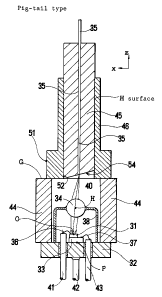
Fig.12 is a section of an embodiment of a PD module. The main
improvement is the reciprocal off-axis deviations of the fiber and the PD in
15 regard to the central axis in order to guide the slanting beam emanating from
the oblique-cut fiber through the center (H) of the lens to the center (O) of the
PD along a straight line. The orientation of the oblique-cut fiber is an
important matter. Although this embodiment may appear to be similar to the
prior art of Fig.2, the embodiment of Fig.12 is not fully the same as the module
2() of Fig.2 which aligns the fiber, the lens and the PD on a straight line normal to
the PD surface.
In Fig.12, a header (package) 32 is provided with a submount 33 at the
center of the top surface. A photodiode (PD) chip 31 is die-bonded on the
submounl 33. The header 32 has pins 41, 42 and 43 projecting below. The
25 submount 33 is an insulator with both surfaces metallized (coated with a metal
CA 02227804 1998-01-23
thin film). Thus the top surface is insulated from the bottom surface in the
submount. The p-electrode of the PD chip 31 is connected by a wire 36 to the
pin 41. l[he n-electrode of the PD is bonded upon the submount 33. The
top of the ~submount 33 is connected to the pin 43 with a wire 37. The center
S of the PD chip 31 does not lie on the center of the header 32. The center (O)of the PD chip 31 deviates by a certain distance in a horizontal direction from
the center of the header 32. The deviation x of the PD on the header is given
by x=Ltan cY, where L is the distance between the center of the lens and the PD
and ~r is the slanting angle of the emanating beam to the central axis which
10 is a line normal to the PD. The PD chip 31 should be die-bonded at a point
deviating for x=Ltan c~ from the package center.
A cap 38 has a window having a ball lens 34. The cap 38 is fitted on
the header 32 at a central position. The center (H) of the lens 34 coincides
with the center (P) of the header 32 in the vertical direction. Z-axis is
15 defined as a normal line standing on the header 32 and including the center (H)
of the lens 34. Of course, there may be some unknown error of mounting the
cap on the header. The error is now neglected in the following description,
because the error can safely be absorbed by an alignment of the fiber. A
cylindrical sleeve 44 is welded upon the header 32. A ferrule 45 cramps an
20 end of an optical fiber 35. The end 54 of the ferrule with the fiber is ground
obliquely at an angle ~ for preventing the reflection light from returning the
laser. A~ point 52 is the lowest point of the ferrule end. The oblique angle
is, in general, 5 ~ to 1n ~ . This example adopts 8 ~ of the oblique-
cutting.
~ =8 ~ gives cY =3.9 ~ . The vertical distance L between the lens
36
CA 02227804 1998-01-23
center (H) and the chip is determined by the size of the cap 38. Here L=2000
,um (2mm'~. The PD should be fixed at a point deviating by x=-136,~m (Ltan
~) from the center (P) of the header. Such an off-axial bonding of the PD
may be called an "offset mounting". Alternative mounting is deviating the
5 lens by +136,u m and coinciding the PD center with the header center.
Generally the PD should be deviated from the lens by x=-Ltan cY . It is,
however, convenient for alignments to keep the lens on the axis and deviating
the PD.
Thl- ferrule 45 is inserted into a ferrule holder 46. The ferrule holder
10 46 is welcled upon the end surface (G) of the sleeve 44. The center of the
ferrule holder 46 does not lie above the center (P) of the header 32. The
ferrule holder 46 deviates from the central axis (Z-axis) in the direction
contrary to the deviation of the PD chip 31. Besides, the lowest edge (S) is
the closest to the axial line (Z-axis) among any points of the oblique-cut end
15 40 of the fiber 35. The orientation is important. This is the iso-orientation
which has previously been defined. A mark 51 is drawn on the side of the
ferrule holder 46 for showing the direction of the lowest edge (S). The mark
51 teaches us the orientation of the fiber. The iso-orientation of Fig.12 can
be accomplished by coinciding the mark 51 with an imaginary plane including
2() the lens c~ nter (H) and the PD center (O) and being vertical to the header plane
(XY-plane).
The alignment of the fiber includes an axial adjustment in the Z-
direction, a parallel displacement in XY-plane and a rotational adjustment
around the fiber axis. The three kinds of alignments can determine the
25 optimum location of a fiber in a PD module. The axial adjustment means an
CA 02227804 1998-01-23
axial sliding of the fiber in the Z-direction in the ferrule for seeking an
optimum point which makes Gauss' image of the fiber end at the back of the
PD and gi~les sufficient light power to the PD. Namely, the axial adjustment
determines the fiber end at a defocused spot, keeping the maximum sensitivity
of the PD in compliance with the mentioned prior application No.6-171873.
Here assuming that the axial adjustment has already been done, two other
adjustmenl s of the xy-parallel displacement and the rotation adjustment are
explained in detail.
Conventionally, the alignment in a certain plane parallel with XY-plane
10 includes the parallel displacement and the rotation. Namely conventional
alignments in XY-plane = parallel displacement + rotation. Fortunately, this
invention can dispense with the rotation adjustment in some cases.
Otherwise, this invention can simplify the rotation adjustment in other cases.
The first step is the search of the spot which gives the maximum light
15 power (highest sensitivity) and the minimum distortion (smallest IMD2) to thePD by displacing the ferrule holder 46 in parallel on the end surface of the
sleeve 44. During the parallel displacement, the output of the PD is
monitored. The second step is the investigation of the orientation of the
fiber by rotating the fiber 35 with the ferrule holder 46 for seeking the
20 orientation which realizes the minimum distortion IMD2. When the optimum
orientation is identified, the ferrule holder 46 is fixed to the sleeve 44 at the
position and at the orientation. This invention can alleviate the time of the
rotation adjustment to a great extent, since the preferable orientation of the
fiber has been predetermined so as to dispose the lowest edge (S) closest to the25 axial line. In any case, the rotation adjustment can be done within 90 degrees
38
CA 02227804 1998-01-23
at most. [n some cases, this invention can do without the rotation adjustment
at all. In short, the alignment of the invention in XY-plane = parallel
displacement + restricted rotation. Or the alignment = parallel displacement.
The omission of the rotation adjustment in a full range of 360 degrees
5 alleviates l~he time of the alignment.
Ideally the alignment of the fiber should be carried out by monitoring
both the power and the distortion of the PD. But, it is a well known fact that
the input power has a maximum value in a wide range, as shown in Fig.4.
Then the alignment can be done by monitoring only the distortion. The
10 distortion is more important than the sensitivity in PDs.
In an ideal coordination, the central beam emanating from the fiber end
(Q) with a slanting angle of c~ should pass the lens center (H) and should
shoot the PD center (O). Manufacturing errors may divert the central beam
from (H) and (O) in products. The position and the orientation of the fiber
15 are actually determined by three or two kinds of alignments for seeking the
minimum distortion and the maximum sensitivity. Thus, it is not necessary
that QHO is an exactly straight line. But in any case, the points (Q),(H) and
(O) align nearly on a direct line in actual PD modules manufactured by this
invention
2()
39