Note: Descriptions are shown in the official language in which they were submitted.
CA 02227933 2007-03-13
PHASING AND INDICATOR ARRANGEMENTS FOR SWITCHGEAR OR THE LIKE
BACKGROUND OF THE INVENTION
Field of the Invention
The present invention relates generally to phasing and indicator arrangements
for
switchgear and the like in the field of electrical power distribution, and
more particularly to an
arrangement that facilitates phasing measurements with the use of conventional
voltmeters and
an indicating arrangement with desirable test features.
Description of the Related Art
In the field of electrical power distribution, it is a common practice to
perform phasing
measurements between various power cables to determine the phase difference
between and the
correct connection of the power cables throughout the system. Various prior
art arrangements
include indicator lights that respond to sensed voltage signals to indicate
whether two signals are
in phase or out of phase. For example, device types HO-MPKTM and HO-PVTM are
available
from ELSICTM, Trompeterallee, Germany. Further, page 14 of Merlin Gerin
Publication
AC0063/3E illustrates voltage indicator lamps and a phase concordance unit
designated MX
403TM.
Additionally, various devices are known that respond to voltage sensors and
that function
as voltage indicators. An arrangement for testing the integrity of the voltage
sensing system is
shown in U.S. Patent No. 5,521,567.
While these prior art arrangements may be useful to provide various indicator
and
phasing arrangements, the prior phasing arrangements are rather awkward to
operate, require
manipulation and interconnection of various components, require relatively
expensive sensing
devices, require the use of specialized meters or devices, and/or require
external power supplies.
Further, the prior indicator arrangements require separate power supplies for
testing and do not
provide simplified unambiguous self-testing functions.
-1-
CA 02227933 1998-01-26
SC-5287-C
SUMMARY OF THE INVENTION
Accordingly, it is a principal object of the present invention to provide an
arrangement
that is responsive to a voltage sensor and determines phase information that
is measurable with
a voltmeter.
It is another object of the present invention to provide a method to verify
phasing
between different electrical sources with the use of a voltmeter and such that
the phasing
determination is independent of the source voltage.
It is a further object of the present invention to provide a phasing
arrangement that is
responsive to two or more alternating current sources and that provides
phasing information as
the AC voltage between outputs representing each of the two of the altemating-
current sources.
These and other objects of the present invention are efficiently achieved by
the
provision of a phasing and indicator arrangement that responds to electrical
sources and
provides voltage indicator functions, phasing determinations, and self-test
features.
Phasing provisions are responsive to two or more voltage sensors proximate
respective
electrical sources to provide an output that represents the phase difference,
i.e. time
relationship, between the electrical sources as an altemating-current voltage
measurable by a
'voltmeter. The output is relatively independent of the voltage of the
electrical sources.
The indicator arrangement is operable in a test mode to test the integrity of
one or more
voltage indicators while clearly identifying that the indicator arrangement is
in a test mode. In
a preferred arrangement, the indicator arrangement in the self-test mode is
powered by a
photocell. Further, in the self-test mode, the indicator arrangement generates
signals through
each voltage sensor and over the complete voltage sensing path, the generated
signals being
substantially similar to the signals generated by each voltage sensor during
normal operation in
i-esponse to an alternating-current source. In the self-test mode, the phasing
arrangement is
;dso tested.
BRIEF DESCRIPTION OF THE DRAWING
The invention, both as to its organization and method of operation, together
with
fiurther objects and advantages thereof, will best be understood by reference
to the specification
taken in conjunction with the accompanying drawing in which:
-2-
CA 02227933 1998-01-26
SC-5287-C
FIG. 1 is a block diagram representation of a phasing arrangement of the
present
invention;
FIG. 2 is a diagrammatic representation of various signals in the phasing
arrangement
of FIG. 1;
FIG. 3 is a diagrammatic representation of an indicator or display arrangement
which
uitilizes the phasing arrangement of FIG. 1; and
FIG. 4 is a block diagram electrical schematic diagram of portions of the
indicator or
display arrangement of FIG. 3.
DETAILED DESCRIPTION
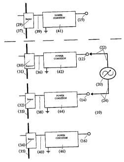
Referring now to FIG. 1, the phasing arrangement 10 of the present invention
provides
phasing outputs at 12, 14, and 16, e.g. corresponding to a three-phase
alternating-current
electrical system. The outputs 12, 14 and 16 provide phase information that
corresponds to
each of the respective phases or electrical sources 31, 33 or 35 of the
electrical system while
being relatively independent of the voltage on each phase. An alternating-
current voltmeter 20
with leads 22, 24 placed across two of the phasing outputs measures the phase
difference, i.e.
time relationship, e.g. as a voltage generally proportional to the phase
difference.
The phasing arrangement 10 includes sensors 30, 32 and 34 that provide
respective
outputs 36, 38 and 40 which are proportional to the associated respective
electrical source or
phase line 31, 33 or 35 of the electrical system. Each of the outputs 36, 38
and 40 is
connected to the input of a respective power conditioning stage 42, 44 and 46.
In a specific
ernbodiment, the outputs 36, 38 and 40 are high-impedance outputs such that
the power
conditioning stages 42, 44 and 46 isolate the high impedance outputs 36, 38,
and 40 of the
sensors 30, 32 and 34 and provide the phasing outputs 12, 14 and 16. In a
specific
ernbodiment, the outputs 36, 38 and 40 are sinusoidal waveforms representative
of the
electrical sources. The power conditioning stages 42, 44 and 46 convert each
of the sinusoidal
waveform outputs at 36, 38 and 40, via clamping action or the like, to
waveforms at the
ptiasing outputs 12, 14 and 16 that are substantially square waves.
With additional reference now to FIG. 2, the waveforms 70, 72 and 74 represent
the
signals at the respective phasing outputs 12, 14 and 16, the waveforms 70, 72
and 74
containing the phase information of the respective electrical sources or phase
lines 31, 33 and
sensed by the respective sensors 30, 32 and 34.
The waveform 76 in FIG. 2 corresponds to a fourth phasing output 15 in FIG. 1
of
another electrical source 37 sensed by a sensor 29 having an output 39
connected to a power
-3-
CA 02227933 1998-01-26
SC-5287-C
conditioning stage 41, the power conditioning stage 41 providing the phasing
output 15. For
example, in a specific illustration, the electri;cal source 37 represents
"phase one" of a "second
way" or 3-pole circuit path of the electrical system while the electrical
source 31 represents
"phase one" of a"fi,rst way" or 3-pole circuit path.
Before connecting the electrical sources 31 and 37 together via a switch or
the like, the
phase relationship between the two sources 31 and 37 is determined or verified
via measuring
the voltage between the respective phasing outputs 12 and 15 which are
represented by the
respective waveforms 70 and 76. If the voltage difference measured on the AC
voltmeter 20 is
below a predetermined level, the electrical sources 31 and 37 of the two ways
are suitable for
connecting to the same bus. However, if the voltage difference is above a
predetermined level
establishing that a significant phase difference exists between the two
sources, the two
electrical sources should not be interconnected. Accordingly, in accordance
with important
aspects of the present invention, the phase difference between various
electrical sources can be
nieasured via the voltage between the corresponding phasing outputs.
As illustrated in FIG. 2, the two waveforms 70 and 76 (cerresponding to
electrical
sources 31 and 37) are of relatively the same phase or time relati ;n 7} 3nd
are thus suitable
for interconnection. For example, if the two electrical sources 31 a,:- Ile
exactly in phase,
i.e. 0 degrees phase difference, then the voltage measured between the --ig
outputs 12 and
15 would be essentially zero volts. On the other hand, the phase differt..
)etween the two
electrical sources 31 and 33 is significant (as illustrated in FIG. 2 by
wavetu. ms 70 and 72).
T'hus these two electrical sources 31 and 33 are not suitable for
interconnection, which can be
ascertained via the measurement of the voltage differential between the
corresponding phasing
outputs 12 and 14. Specifically, as shown in FIG. 2, the two electrical
sources 31 and 33 are
approximately 120 degrees out of phase with respect to each other and in the
example
correspond to two different phases of the first way of the electrical system.
For illustrative purposes not to be interpreted in any limiting sense, it has
been found
that the phasing outputs operate in a desirable fashion for a voltage range of
approximately 15-
38kv (phase-to-phase) AC and such that no calibration or adjustment is
required to measure the
phase differential using the phasing outputs, the magnitude of the waveforms
in FIG. 2 being
approximately 15 volts peak-to-peak. In a particular example, if the phasing
output 12 to
ground measures V1 to ground, the voltage from output 12 to output 14 is
approximately V1
times the square root of 3. Further, the voltage differential between phasing
outputs 12, 15 is
less than (V1)/3 for the illustration where the waveforms 70, 76 are less than
10 degrees out of
phase with respect to each other. As stated in other terms, the phasing
arrangement 10 of the
-4-
CA 02227933 2007-03-13
present invention establishes a voltage between the phasing outputs that
characterizes or
establishes a relationship between the measured AC voltage and the phase
difference (time
relationship) between the sensed electrical lines, i.e. a predetermined
function between phase
difference and voltage. As noted, it should also be understood that the
phasing outputs 12, 14,
16 and 15 can also be utilized to verify the presence of voltage of the
electrical sources, i.e.
via the voltage measured phase to ground. It should also be understood that in
specific
embodiments of the present invention where additional accuracy of the phase
differential
measurement is desired, the power conditioning stages 41, 42, 44 and 46
include additional
wave shaping circuitry to provide waveforms that are more accurately measured
by AC
voltmeters and the like.
Referring now additionally to FIGS. 3 and 4, in a specific embodiment, the
phasing
arrangement 10 is provided as an integral part of an indicator or display
arrangement as
represented by 50 in FIG. 3. In an illustrative embodiment, not to be
interpreted in any
limiting sense, the indicator arrangement 50 is utilized as the display panel
referred to as item
40 in the aforementioned United States Patent Nos. 5,864,107; 6,040,538; and
6,114,642 to
provide information about the status of the circuit and components of the
switchgear 20 shown in
that application such as the energized/deenergized status of each pole of the
overlied load
interrupter switch or fault interrupter.
For example, as shown in FIG. 3, the indicator arrangement 50 includes, for
each pole,
a voltage indicator 52 and a line diagram 54 representing the electrical
circuit and the load
interrupter switch or fault interrupter (a load interrupter switch being
illustrated in FIG. 3). A
test indicator 60 and the voltage indicator 52 provide information on the
operable status of the
indicator arrangement 50 and the integrity of the voltage sensing system for
each pole.
Reference may be made to U. S. Patent No. 5,521,567 for a further discussion
of the testing
of the integrity of the voltage sensing system. The phasing outputs 12, 14 and
16 are provided
for each respective phase of the circuit illustrated at pins or posts 112,
114, and 116.
In the illustrative example of the indicator arrangement 50, the test
indicator 60
displays a predetermined test symbol, e.g. a solid circle, when the indicator
arrangement 50 is
appropriately sequenced for testing. In the specific illustration, for testing
purposes, a solar
panel (i.e. photocell) 64 is provided to power the indicator arrangement 50.
Additionally a
test actuator 66 is provided that includes a transparent window over an
optical switch at 66.
The test sequence is actuated in response to the blocking of light to the
optical switch at 66
while the solar panel 64 is illuminated sufficiently to provide power to
actuate the indicator
arrangement 50 and test circuit. Thus, after the user covers the test actuator
66, the display of
-5-
CA 02227933 2007-03-13
the test symbol in the test indicator 60 provides assurance that the indicator
arrangement 50 is
appropriately powered up and fully functioning. With the test indicator
displayed at 60, the
user may then ascertain the operability of each voltage indicator 52 and the
integrity of the
voltage sensing circuit for that corresponding pole. Thus, the presence of the
test symbol at 60
and the three voltage indicators at 52 assure that the overall voltage sensing
system is
functioning appropriately.
In a specific embodiment, the voltage indicator 52 flashes the energized
symbol, e.g.
lightning bolt or the like, in the test mode to verify that the voltage
indicator 52 is functional
and the voltage sensing circuit is fully functional and reliable. Following
this test function,
i.e. after the operator unblocks the transparent window over the optical
switch at 66, the
energized/deenergized status of each pole may then be ascertained via the
status of the voltage
indicator 52 provided for each respective pole, for example 52b and 52c for
the respective
second and third poles of the indicator arrangement 50. In a specific
embodiment, while the
voltage indicators 52 are arranged for normal functioning, the operator before
relying on the
absence of an energized symbol at the voltage indicator 52, activates the
testing mode of the
indicator arrangement via the feature at 66 and observes the test symbol at 60
and checks for
the presence of the energized symbols at 52a, 52b and 52c to determine proper
operation.
Without such appropriate testing, the voltage indicators 52 in themselves
would function only
as ordinary indicators as found in the prior art.
Referring now additionally to FIG. 4, the testing circuit 90 of the indicator
arrangement 50 is powered by the solar panel 64 and actuated by the test
actuator feature at
66. When the optical switch 92 is turned off by the blocking of light at 66,
the optical switch
92 via path 94 activates a power regulator stage 96. The power regulator stage
96 supplies
power to the power converter and signal generator stages referred to at 98
which actuate the
test indicator 60 with a suitable alternating wave signal at 100. The
alternating wave signal at
100 via a surge protection stage 102 provides signals for each phase at 104
which are
connected to the sensors 30, 32 and 34. This signal path tests the integrity
of the overall
sensing circuit. If the sensing path is fully functioning, the signal will be
returned at 106 on
the lines from the bushing sensors 105. The signal at 106 is then processed by
a power condition
and logic stage 108 which provides protection and the desired indicator
waveform at 110 to drive
the voltage indicator 52, e.g. a flashing signal.
Accordingly, the testing circuit 90 of the indicator arrangement 50 when
actuated by
the test actuator feature at 66 checks the integrity of the signal paths from
the sensor and
activates the voltage indicators at 52 to also test the integrity of the
voltage indicators 52. As
-6-
CA 02227933 1998-01-26
SC-5287-C
discussed hereinbefore, if any of the voltage indicators 52 are not actuated
during the testing
mode with the testing indicator 60 actuated, the operator is alerted that the
voltage indicators
52 are not working and not to be relied upon.
The power condition and logic stage 108 also is arranged to provide
appropriate
phasing signals at the phasing outputs 12, 14 and 16 as explained
hereinbefore, such that the
phasing outputs provide phasing information that is independent of the sensed
voltage levels
and such that an alternating-current voltmeter may be utilized to measure the
phase difference
between the phases or electrical sources 31, 33 or 35 of the electrical
system. It should also be
noted that the phasing outputs 12, 14 and 16 are also tested in the test mode
of the indicator
arrangement 50, i.e. in the test mode, each of the phasing outputs 12, 14 and
16 develop a
voltage to ground that can be measured using the AC voltmeter 20.
For illustrative purposes not to be interpreted in any limiting sense, it has
been found
that the indicator arrangement 50 along with the phasing outputs operates in a
desirable fashion
for a voltage range of approximately 4-38kv (phase-to-phase) AC and such that
no calibration
or adjustment is required to provide the indicator functions and testing and
also to measure the
phasing outputs.
While there have been illustrated and described various embodiments of the
present
invention, it will be apparent that various changes and modifications will
occur to those skilled
in the art. Accordingly, it is intended in the appended claims to cover all
such changes and
modifications that i'all within the true spirit and scope of the present
invention.
-7-