Note: Descriptions are shown in the official language in which they were submitted.
CA 02227954 1998-O1-26
- 1 -
"A POWER SUPPLY FOR DISCHARGE LAMPS WITH BALANCED
RESONANT CIRCUIT"
Y
DESCRIPTION
Field of the invention
The present invention relates to a power supply
circuit for discharge lamps of the type comprising a
power supply with inverter and a load circuit, into
:LO which the lamp is inserted, and which has an LC type
resonant circuit in series with the electrodes of the
lamp.
State of the art
Circuits for the power supply of discharge
:L5 lamps of the type mentioned above are known in the art.
Examples of such circuits can be found for example in
EP-A-O 610 642, EP-A-O 113 451, NL-A-9000175.
Represented in Fig. 1 is a simplified diagram
of a circuit for the power supply of a discharge lamp 1.
:ZO The circuit has an inverter section,
generically indicated by 1, made in a manner known par
se to those skilled in the art and not described in
greater detail. This typically has two electronic
circuit breakers in a half-bridge arrangement which are
:25 alternately switched on and off. Upstream of the
inverter is arranged a rectifier bridge (not shown)
interposed between the power supply network and the
inverter.
Between the lamp 1 and the inverter 1 is
:30 arranged an LC type oscillating circuit with an
inductance L arranged between a first pole 3 of the
inverter 1 and a first electrode 5 of the lamp 1 and
with a capacitance C between the second pole 7 of the
inverter 1 and the second electrode 9 of the lamp 1. Cs
:35 indicates a capacitor in parallel with the lamp 1.
Upon ignition the inductance L and the
capacitance CZ in parallel with the lamp resonate such
that an alternating voltage With a high peak value, of
the order of 1000 V is developed between the electrodes
CA 02227954 1998-O1-26
and 9. Following ignition of the lamp, a potential
difference of around 100 V is developed between the
electrodes 5 and 9 and resonance occurs between the
inductance L and the capacitance C. Under these
5 conditions the voltage at the point P1 is given by the
sum of an alternating voltage which oscillates between
-200 and +200 V approximately, and a constant voltage
of approximately +200 V, whereas at the point P2 the
voltage is given by the sum of a voltage oscillating
between approximately -30 V and +30 V and a constant
voltage of approximately 200 V. The two waveforms of
the voltage at the points P1 and Pa are represented
diagrammatically in the two graphs on the right of
Fig.l. Specifically, therefore, the point P1 exhibits a
1.5 potential to earth which varies greatly between two
positive and negative values, whereas the potential at
the point PZ oscillates slightly about a constant value.
This entails a differing leakage of current to earth
through the effect of the stray capacitances of the
load circuit.. Consequently, the current which passes
through the lamp is not the same along the whole length
of the latter. Since the electrode 5 undergoes a much
higher voltage variation than the electrode 9 not all
of the current which leaves the electrode 5 reaches the
electrode 9, rather some of it leaks away through the
effect of the stray capacitances. Consequently this
gives a non-constant brightness of the lamp, especially
noticeable in the case of a "dimmed" lamp; i.e. when
the lamp is operated at a lower luminous intensity than
the maximum allowed.
The effect of the leakage capacitances is even
more noticeable in the case in which two lamps are
placed in series in the same circuit. In this case, to
avoid unacceptable variations in brightness along the
extent of the two lamps, a particularly complex circuit
solution of the type shown in Fig. 2 is currently
resorted to. The lamps are indicated by 11 and lz,
whilst Lland LZ indicate two inductances which resonate
with the capacitance C. C2' and C2" indicate the two
CA 02227954 1998-O1-26
7 - 3 -
capacitances in parallel with the lamps L1 and L2. The
power supply inverter represented diagrammatically is
again indicated by 1. -Essentially, when the load
R
circuit provides for the application of two lamps. the
resonant circuit is divided. In order to have the same
current in both resonant circuits there is provision
for the addition of a compensation transformer
indicated generically by 11, whose common-core windings
belong to the two resonant circuits associated with the
lamps li and 12 respectively.
This circuit solution avoids the non-uniformity
of brightness of the two lamps in series, but entails a
high cost of the circuit, in so far as the two lamps
are associated with two independent resonant circuits
and furthermore the use of three magnetic components is
required, the third of which (the transformer 11)
entails an appreciable increase in the overall cost of
the circuit.
Summary of the invention
The purpose of the present invention is to
produce a circuit for the power supply of discharge
lamps which avoids the drawbacks of conventional
circuits.
More particularly the purpose of the present
invention is to produce a circuit for discharge lamps
which makes it possible, With simple and economical
structural solutions, to avoid variation in brightness
along the lamp, even in the dimmed lamp condition. A
further purpose of the present invention is to produce
a particularly simple circuit which makes it possible
to power two or more lamps in series without additional
magnetic elements, with a single oscillating circuit
and while eliminating the variation in brightness of
the lamps in series.
These and further purposes and advantages which
will become clear to those skilled in the art from
reading the text which follows are obtained essentially
by providing for the LC resonant circuit in series with
the lamp to be a balanced resonant circuit. Balanced
CA 02227954 2004-O1-27
20333-417
4
is understood to mean a circuit in which the values of
capacitance and inductance between the lamp and the two
terminals of the inverter are substantially equal.
This is obtained in particular for example by
arranging an inductance and a capacitance between one pole
of the inverter and the first electrode of the lamp, and a
second capacitance and a second inductance between the other
electrode of the lamp and the second pole of the inverter.
When there are two lamps, they can be arranged in series
with each other and in series with a single resonant circuit
with the same configuration as described above.
In this way an oscillation in voltage between the
same maximum and minimum values occurs at the two terminals
of the lamp, or at the two terminals or an assemblage of two
or more lamps in series. The leakage of current through the
effect of the stray capacitances is therefore uniform along
the entire lamp or along the lamps in series, thereby
obtaining constant brightness under any operating
conditions.
According to the invention the two inductances are
wound on the same core. In this way the power supply
circuit contains a single magnetic component and is
particularly economical and compact.
In summary, according to one aspect the invention
provides a circuit for the power supply of a discharge lamp,
the circuit comprising: an inverter which provides an
alternating voltage across a first pole and a second pole;
and a load circuit connected to the inverter, the load
circuit including a first and second connection for a
discharge lamp and a resonant circuit in series with the
first and second connections for a discharge lamp, the load
CA 02227954 2004-O1-27
20333-417
' ~ 4a
circuit receiving the alternating voltage from the invert;
wherein the resonant circuit includes: a first capacitance
and a first inductance arranged between the first pole of
the inverter and the first connection for a discharge lamp;
and a second capacitance and a second inductance arranged
between the second pole of the inverter and the second
connection for a discharge lamp; wherein the resonant
circuit is balanced; and wherein the first and the second
inductances are wound onto one winding core.
According to another aspect the invention provides
a ballast assembly comprising: an inverter with a first pole
and a second pole across which an alternating voltage is
applied; a load circuit connected to the inverter and having
a first and second connection for a discharge lamp; and a
discharge lamp connected between the first and second
connections for a discharge lamp; wherein the load circuit
includes a resonant circuit in series with the first and
second connections of the load circuit, the load circuit
receiving the alternating voltage from the inverter; wherein
the resonant circuit includes: a first capacitance and a
first inductance arranged between the first pole of the
inverter and the first connection for a discharge lamp; and
a second capacitance and a second inductance arranged
between the second pole of the inverter and the second
connection for a discharge lamp; wherein the resonant
circuit is balanced; and wherein the first and the second
inductances are wound onto the same winding core.
Further advantageous embodiments of the circuit
according to the invention are indicated in the attached
claims.
CA 02227954 2004-O1-27
20333-417
' 4b
Brief description of the drawings
The invention will be better understood by
following the description and the appended drawing which
shows a practical non-limiting example of the circuit
according to the invention. In particular the drawing
shows:
In Figs. 1 and 2, two circuit solutions
respectively with one lamp and with two lamps according to
the prior art, as described above;
CA 02227954 1998-O1-26
_ , - 5 -
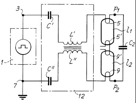
In Fig. 3, a power supply circuit according to
the invention with two lamps in series.
Detailed description of an-embodiment of the invention
In the circuit of Fig. 3 parts which are
identical or which correspond to those of the above-
described circuits of Figs. 1 and 2 are indicated with
the same reference numerals. More particularly, 11 and
lz indicate two discharge lamps in series, powered by a
power supply with inverter 1, of which only a
.LO diagrammatic representation is given and the two
connections of which are indicated by 3 and 7.
A capacitance Cz is arranged in parallel with
the lamps 11 and lz . The electrodes of the lamp 11 are
indicated by 5 and 5' and the electrodes of the lamp 12
are indicated by 9 and 9'.
Arranged in series with the assemblage
consisting of the two lamps 11 and 12 and of the
corresponding capacitor in parallel Cz is a resonant
circuit generically indicated by 12, which between the
pole 3 of the power supply 1 and the electrode 5 of the
lamp 11 comprises a first capacitance C' in series with
a first inductance L'. A second capacitance C " in
series with a second inductance L " is arranged between
the pole 7 and the electrode 9. The two inductances L'
and L " are integrated and wound on the same winding
core. The two capacitances C' and C " have
substantially equal values as do also the two
inductances L' and L " , so that the resonant circuit 12
is perfectly balanced with respect to the load and
consequently an oscillation of voltage between two
substantially equal values with a consequent cancelling
out of the inhomogeneity of brightness of the lamps on
account of the stray capacitances occurs at the points
Pl and P2 of the load circuit.
The same configuration can be used in a circuit
for powering a single lamp 1 which in this case will be
arranged between the electrodes 5 and 9, with the
capacitance CZ in parallel therewith and the balanced
CA 02227954 1998-O1-26
- 6
resonant circuit 12 between the lamp and the power
supply with inverter 1.
It is to be understood that the drawing shows
merely one example given solely by way of practical
demonstration of the invention, it being possible for
the invention to vary in its forms and arrangements
without however departing from the scope of the concept
which underlies the invention. The possible presence
of reference numerals in the enclosed claims has the
purpose of facilitating the reading of the claims with
reference to~the description and the drawing, and does
not limit the scope of the protection represented by
the claims.