Note: Descriptions are shown in the official language in which they were submitted.
CA 02228l3l l998-0l-28
W O 97/05709 PCT~US96/12531
ADAPI'IVE DESPREADER
BACKGROUND OF THE INVENTION
5 I. Field of the Invention
The present invention relates to communication systems. More
particularly, the present invention relates to a novel and improved method
and apparatus for enhancing the performance of direct sequence spread
10 spectrum receivers in the presence of unresolved multipath fading.
II. Description of the Related Art
Communication systems have been developed to allow transmission
15 of information signals from a source location to a physically distinct user
destination. Both analog and digital methods have been used to transmit
such information signals over communication channels linking the source
and user locations. Digital methods tend to afford several advantages
relative to analog techniques, including, for example, improved immunity
20 to channel noise and inL~ ce, increased capacity, and improved security
of communication through the use of encryption.
In transmitting an information signal from a source location over a
communication channel, the information signal is first converted into a
form suitable for efficient transmission over the channel. Conversion, or
25 modulation, of the information signal involves varying a parameter of a
carrier wave on the basis of the information signal in such a way that the
spectrum of the resulting modulated carrier is confined within the channel
bandwidth. At the user location, the original message signal is replicated
from a version of the modulated carrier received subsequent to propagation
30 over the channel. Such replication is generally achieved by using an
inverse of the modulation process employed by the source transmitt~r.
Modulation also facilitates multiple-access, i.e., the simultaneous
transmis~sion of several signals over a common th~nn~l Multiple-access
communication systems will often include a plurality of remote subscriber
35 units requiring intermittent service of relatively short duration rather than continuous access to the communication channel. Systems designed to
enable communication over brief periods of time with a set of subscriber
units have been termed multiple access communication systems.
A particular type of multiple access communication system is known
40 as a spread spectrum system. In spread spectrum systems, the modulation
CA 02228131 1998-01-28
W O 97/OS709 PCT~US96/12531
technique lltili7erl results in a spreading of the trancmitterl signal over a
wide frequency band within the communication channel. One type of
multiple access spread spectrum system is a code division multiple access
(CDMA) modulation system. Other multiple access communication system
5 techniques, such as time division multiple access (TDMA), frequency
division multiple access (FDMA) and AM modulation schemes such as
amplitude companded single sideband are known in the art.
However, CDMA has significant advantages over these modulation
techniques for multiple access communication systems. The use of CDMA
10 techniques in a multiple access communication system is disclosed in U.S.
Patent No. 4,901,307, entitled "SPREAD SPECTRUM MULTIPLE ACCESS
COMMUNICATION SYSTEM USING SATELLITE OR TERRESTRIAL
REPEATERS", and U.S. Patent No. 5,103,459, entitled "SYSTEM AND
METHOD FOR GENERATING SIGNAL WAVEFORMS IN A CDMA
15 CELLULAR TELEPHONE SYSTEM", both are assigned to the assignee of the
present invention, and both are incorporated by reference herein.
In a CDMA cellular telephone system, the same frequency band is
used for communication in all cells. The CDMA waveform properties that
provide processing gain are also used to discriminate between signals that
20 occupy the same frequency band. Furthermore, the high speed pseudonoise
(PN) modulation allows many different propagation paths to be separate,
provided the difference in pathways exceed the PN chip duration, or
one/bandwidth. If a PN chip rate of 1 MHz is employed, multiple path
demodulation can be employed against paths that differ by more than one
25 microsecond in path delay from the desired path. A one microsecond path
delay differential corresponds to differential path distance of 1,000 feet. The
urban environment typically provides differential path delays in excess of
one microsecond, and up to 10-20 microseconds are reported in some areas.
In narrow band modulation systems, such as the analog FM
30 modulation employed by conventional cellular telephone systems, the
existence of multiple paths can result in severe fading characteristics. With
wide band CDMA modulation, however, the different paths may be
discriminated in the demodulation process. This discrimination greatly
reduces the severity of multipath fading. Multipath fading is not totally
35 eliminated in using CDMA discrimination techniques, because there will
occasionally exist paths with delayed differentials of less than the minimum
path delay for the particular system. Signals having path delays on this
order cannot be discriminated against in the demodulator. It is, therefore,
CA 02228131 1998-01-28
W O 97/05709 PCT~US96112531
desirable that some form of diversity exist which would permit a system to
be utilized in order to further reduce the effects of fading.
The deleterious effects of fading can be controlled somewhat by
controlling transmitter power in the CDMA system. A system for cell-site
5 and mobile unit power control is disclosed in U.S. Patent No. 5,056,109,
entitled "METHOD AND APPARATUS FOR CONTROLLING
TRANSMISSION POWER IN A CDMA CELLULAR MOBILE TELEPHONE
SYSTEM", assigned to the Assignee of the present invention and
incorporated by r~rer~lce herein. Furthermore, the effect of multipath
10 fading can be reduced in the hand-off mode when the mobile unit is
transitioning between cell-site service area with the mobile unit
communicating cell-sites during the hand-off process. The hand-off scheme
is disclosed in U.S. Patent No. 5,101,501, entitled "SOFT HANDOFF IN A
CDMA CELLULAR TELEPHONE SYSTEM", assigned to the assignee of the
15 present invention and incorporated by refel~llce herein.
The existence of multipaths can provide path diversity to a wideband
CDMA system. If two or more paths are available with greater than one
microsecond differential path delay, two or more receivers can be employed
to separately receive the signals. Since these signals will typically exhibit
20 independence in multipath fading (i.e., they usually do not fade together),
the outputs of the two receivers can be diversity combined. A method and
apparatus for implementing a combining receiver of this sort is described in
detail in U.S. Patent No. 5,109,390, entitled "DIVERSITY RECEIVER IN A
CDMA CELLULAR TELEPHONE SYSTEM", assigned to the assignee of the
25 present invention and incorporated by lefere~-ce herein.
SUMMARY OF THE INVENTION
The present invention is a novel and improved method and
30 apparatus for enhancing the performance of direct sequence spread
spectrum receivers in the presence of unresolved multipath fading. The
present invention is an alternative to the diversity receiver structure,
described in the aforementioned U.S. Patent No. 5,101,501, for direct
sequence spread spectrum receivers. The present invention is similar in
35 function to the divel~iLy receiver, but it has the advantages of simplicity and
improved performance in the presence of unresolved multipath. It is also
more appropriate for high data rate systems, which may be desirable in
indoor applications. Its novelty lies in the incorporation of a despreading
and re-spreading operation within a traditional adaptive equalizer.
CA 02228131 1998-01-28
W O 97105709 PCT~US96/12531
The multipath propagation channels found in indoor environments
in the 800 to 2000 MHz range typically have rather short delay spreads. The
spread can range from approximately 20 ns to 300 ns depending on the size
of the building, the nature and design of the walls, and other factors. The
5 diversity receivers that are used for direct sequence reception in the cellular
outdoor environment are most effective when the delays between
multipath components are large compared to a spreading sequence chip. In
the standardized CDMA design, as described in detail in the aforementioned
U.S. Patent Nos. 4,901,307 and 5,103,459, the chip duration is approximately
10 800 ns long. The long chip duration relative to the delay spread means that
only one demodulated signal of the diversity receiver will be useful.
Moreover, the unresolved multipath will lead to flat Rayleigh fading of the
output from that one demodulated signal of the divel~ily receiver. Thus,
the divel ,iLy receiver gain that is possible with longer delays is not achieved.
The short delay spread indoors suggests that a novel method for
handling the multipath signal is nec~s~ry. The present invention utilizes
an equalizer like structure to achieve this goal. The purpose of the present
invention is to reduce intersymbol inLeLferel,ce, which arises from
multipath propagation. Eq1l~li7Pr~ using the classic least means squares
(LMS) algorithm normally use feedback based on individual symbol
decisions to update tap weights of a transversal filter. The LMS algorithm
estimates the inverse gradient of an error function with respect to the tap
weights, and adjusts the tap weights in a direction opposite to the estimated
gradient. Under reasonable conditions of channel statistics and gain the
filter converges to a state that is effective in mitigating the intersymbol
inLeLfel~ellce. The LMS algorithm is widely used because of its simplicity,
ease of computation, and the fact that it needs no repetition of the data.
However, in the present application, the LMS algorithm is not directly
applicable because of the direct sequence spreading.
In the CDMA cellular and PCS systems, the multipath spread
introduces intersymbol inleLferel~ce not at the symbol time scale (tens of
microseconds), but rather at the chip time scale (tens to hundreds of
nanoseconds). Therefore, the adaptive equalizer of the present invention
functions with feedback of chip-by-chip errors. In order to do this, the data
modulation must be estimated from the despread signal, the error
estimated, and the difference between soft and hard decisions re-spread by
the original pseudonoise sequence before being fed back as a tap weight
correction.
CA 02228l3l l998-0l-28
W O 97/05709 PCT~US96/12~31
The exemplary implementation of the present invention is used in
demodulating a pilot channel. A pilot channel is channel used to provide
basic timing synchronization information and carries no data. The use and
implementation of a pilot channel is described in detail in the
5 aforf~m~ntioned U.S. Patent No. 5,103,459. The present invention can be use
in demodulating other information channels with minor modifications.
leRIEF DESCRIPTION OF THE DRAWINGS
The features, objects, and advantages of the present invention will
become more apparent from the detailed description set forth below when
taken in conjunction with the drawings in which like reference characters
identify correspondingly throughout and wherein:
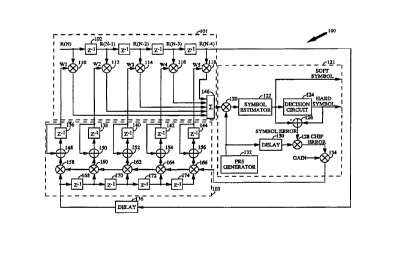
Figure 1 is a block diagram of the present invention.
DETAILED DESCRIPTION OF THE PREFERRED
EMBODIMENTS
FIG. 1 shows the novel adaptive despreader structure which permits
20 equalization of the broadband channel. Not illustrated in FIG. 1 is a receiver
which down converts in frequency the spread spectrum signal and converts
it to a digital baseband signal as is well known in the art. The adaptive
despreader 100 is comprised of: transversal filter 101, least means squares
(LMS) tap updating circuit 103 and symbol estimation, despreading and re-
25 spreading circuitry 121. Adaptive despreader 100 is illustrated as comprisedof discrete elements. In the exemplary embodiment, adaptive despreader
100 is implemented in a microprocessor or micro-controller programmed to
perform the functions described. Though FIG. 1 does not illustrate a
separate timing block it should be noted that such clock timing is typically
30 provided within a microprocessor or micro-controller or could be provided
by an independent timing source.
Transversal filter 101 is a finite impulse response (FIR) filter which
receives the digital signal R, representative of a baseband version of the
spread spectrum signal. Transversal filter 101 generates a filtered signal
35 based upon the most recently received sample R(n), and previously received
samples R(n), R(n-1), R(n-2), R(n-3) and R(n-4). The structure shown in FIG.
1 has five taps. That is the filtered value, S(n) is based upon five received
values R(n), and previously received samples R(n), R(n-1), R(n-2), R(n-3)
and R(n-4) provided to summing element 146. Although, in the exemplary
CA 02228131 1998-01-28
W O 97/05709 PCTrUS96/12531
embodiment, the structure shown is a five tap ~I R filter, any number of taps
may be used consistent with performance requirements.
The received signal is provided to a series of delay elements 102, 104,
106 and 108. In a spread spectrum communication system the smallest piece
of transmitted information is referred to as a chip. ~ach chip has a
predetermined chip period. Each of delay elements 102, 104, 106 and 108
delay the received chip by a value equal to the sampling period of the signal.
In the exemplary embodiment, the input sampling rate is a small integer
multiple of the chip rate. For example a chip rate of 1.25 ME~z, the integer
multiple could be 4 with a corresponding sampling rate of 5 MHz. Delay
elements 102, 104, 106 and 108 may be implemented using latches or other
memory elements which are well known in the art.
The current sample R(n) and output of each of delay elements 102,
104, 106 and 108 are respectively provided to multipliers 110, 11Z, 114, 116
and 118. In multipliers 110, 112, 114, 116 and 118, the sample values are
weighted by weighting tap values w1, w2~w3, w4 and w5, respectively, which
are computed by LMS tap updating circuit 103, described later herein. Each
of the weighted sample values are provided to summer (~;) 146.
Summer 146 sums each of the weighted sample values to generate the
output value, Sn. Summer 146 outputs the filtered values Sn at the chip
rate, that is one per chip period.
The output chip from transversal filter 101, Sn, is provided to symbol
estimation, despreading and re-spreading circuitry 121. The output chip, Sn,
is provided to multiplier 120. In multiplier 120 the input filtered chips Sn
are multiplied by binary digits of a pseudo random sequence provided by
pseudo random sequence (PRS) generator 132 at the chip rate. The product
of multiplier 120 is provided to symbol estimator 122. Symbol estimator 122
integrates the results of the outputs from multiplier 120 over a symbol
period, which is greater than the chip period, in order to generate the
despread symbol. Symbol estimator 122 may be formed from a digital
integrator well known in the art. Symbol estimator 122 may also provide a
symbol mapping, where the illLe~;laLed chip values provide a first symbol
estimate which maps into soft symbol by a predetPrminPd mapping. A
typical mapping is the Hadamard transform mapping.
If the spreading is bipolar phase shift keyed (BPSK), then the
despreading sequence should be bipolar (+1) valued, identical to the
spreading sequence used at the transmitter. If the spreading is quadrature
phase shift keyed (QPSK), then generally its I and Q components should
each be bipolar valued, and the despreading sequence is the complex
CA 02228l3l l998-0l-28
WO 97/05709 PCTrUS96/12531
conjugate of the spreading sequence used by the transmitter. In the
exemplary embodiment, PRS generator 132 is implemented using a shift
register, the design and implementation of which is well known in the art.
The despreading operation yields a low-pass signal component
5 ~olle~onding to the data modulation present in the original transmitted
signal of interest. InLt:lLeL~l.ce from other stations will not be compressed bythe pseudonoise multiplication and will remain a wideband waveform as is
described in detail in the aforementioned U.S. Patent Nos. 4,901,307 and
5,103,459.
Symbol estimator lZ2 operates on the output of summer 146. Symbol
estimator 122 filters or otherwise processes the samples from transversal
filter 101 and generates an estimate of the modulation symbol which was
transmitted during each symbol period. Normally, a large number of chips
affect each symbol, reflecting the large ratio of spreading bandwidth to data
15 rate. This symbol estimator output is labeled 'soft symbol' in FIG. 1.
The soft symbols are further processed by decision circuit 124. The
output of decision circuit 124is a complex value which is a reconstruction of
the original transmitted modulation symbol. In the case of demodulating a
pilot signal, that symbol is represented by a single complex number, such as
20 1 + 0j. In the case of demodulating a pilot signal, decision circuit 124 is acomparator where the integrated chip values provided by symbol estimator
122 are compared to a constant. This implementation of decision circuit 124
is useful in generating an unmodulated pilot estimate. On the other hand,
decision circuit 124 may be a complex circuit such as a Viterbi decoder which
25 supplies re-encoded channel symbols as a result of its final decisions.
An error waveform is calculated as the difference between the soft
decision symbol provided by symbol estimator 122 and the hard decision
symbol provided by decision circuit 124 in summer 146. This complex error,
e(n), is re-spread in multiplier 128 by a pseudo-random sequence provided
30 by PRS generator 132 which is delayed by delay element 130. Delay element
130 may be configured from a latch or memory element known in the art.
Tap weight updates are computed in accordance with the LMS
algorithm in LMS tap updating circuit 103. The original spread signal
samples must be used, not the modulation symbols. This differs from the
, 35 traditional LMS adaptive equalizer in that the signal is despread for symbol
decision making, and re-spread for tap updating.
The structure of decision circuit 124 can have different
implementations depending on its application. IN the exemplary
embo-lim~nt, where a substantial portion of the forward link power is
CA 02228131 1998-01-28
W O 97/05709 PCTAUS96/12531
devoted to a spread but otherwise unmodulated pilot, the transmitted
symbol is known a priori to be a constant. So the output of decision circuit
124 does not depend on the received signal at all, but is simply a constant,
such as 1 + j0. Thus, the soft symbols are short term averages of the
5 despreader output, and the symbol errors are differences between those
short term averages and the constant target.
The symbol decisions are based on the values of many chips. They
are, therefore, not available until some time after the last chip from which
they are comprised. Because of this delay, the received signal, R(n), must be
10 delayed before being provided to LMS tap updating circuit 103 and the
pseudo random sequence must be delayed before being provided to
multiplier 128. Delay element 130 delays the pseudo random sequence and
delay element 176 provides the delay for the received signal, R(n). Those
delays are at least one data symbol in length. The delays will be several
15 symbols if Viterbi decoder side information is used, since final symbol
decisions lag receipt by at least the truncation length of the decoder.
The delays shown in FIG. 1 are there to bring the decision error
feedback into time alignment with the channel samples. They are,
therefore, approximately one symbol in duration. Typical symbol periods
20 are 52.1,us. on the forward link and 208.3 ~LS on the reverse link. The
spreading code delay need remember only two bits per chip, or 128 and 512
bits. Thus, the signal samples, at 8X oversampling and 4 bits for I and Q
would need 8192 and 32768 bits, respectively.
In a system with code rate p, m-ary modulation, and data rate R, the
25 symbol period is given by:
T P log2 m (1)
So the delay in terms of samples are computed as:
p log2 m ~f~hip S, (2
Tsymb-fc~ip- R
where S is the oversampling ratio for the signal.
One can compute the number of taps needed in transversal filter 101
35 in terms of the total delay span of the multipath signals. Thus, if the delayspan is set at 200 nanoseconds, then at this sampling rate of 20 MHz the
number of taps can be com~uled as:
CA 02228l3l l998-0l-28
W O 97/05709 PCTAUS96/12531
200 ns ~ 20 MHz + 1 > 5 taps (3)
will be nec~s~ . y.
The success of this scheme depends on the adaptation speed being fast
5 enough to follow the short term changes in apparent multipath, mostly due
to motion of the handset. For a handheld unit the rate of change at 1800
MHz and 3 m/s (6.7 mph) can be estimated to be about 2fv/c = 36 nulls/sec,
or about 28 ms between nulls. This suggests that the adaptation time should
be no more than a few hundred microseconds for the scheme to be
10 successful. At vehicular speeds the time is reduced by about a factor of 10, or
about 2.8 ms.
A fixed gain is shown multiplying the error signal in multiplier 134
before it is provided back to LMS tap updating circuit 103. This gain must be
appropriately chosen, since it may cause slow convergence if it is too small,
15 and causes instability if it is too large.
LMS tap updating circuit 103 receives the weighted error signal from
multiplier 134 and the delayed samples from delay element 176. The
delayed samples from delay element 176 are provided to a series of delay
elements 168, 170, 172 and 174. Delay elements 168, 170, 172 and 174 each
20 delay the received sample by an additional sample period as described in
relation to delay elements 102, 104, 106 and 108.
The outputs from delay elements 176, 168, 170, 17Z and 174 are
provided to multipliers 158, 160, 162, 164 and 166, respectively. The output
of multipliers 158, 160, 162, 164 and 166 are provided to a first input of
25 summers 148, 150, 152, 154 and 156, respectively. The outputs from
summing elements 148, 150, 152, 154 and 156 are provided to delay elements
136, 138, 140, 142 and 144. The second input to summers 148, 150, 152, 154
and 156 is a single sample delayed output of each of the respective summers
136, 138, 140, 142 and 144. Delay elements 136, 138, 140, 142 and 144 delay the
30 input sample by a single sampling period. The outputs from delay elements
136, 138, 140, 142 and 144 are provided as the tap values to transversal filter
101 as provided to multipliers 110, 112, 114, 116 and 118, respectively.
This structure is simpler than a diversity receiver. Only one
demodulator is needed, in contrast to multiple demodulators in the
35 div~ y receiver. There is also no need to search for multipath signals and
to assign demodulation elements to the multipath signals, since the tap
locations are fixed at regular intervals. Because there is no dynamic
assignment, there is no loss due to assignment errors. Since there is only
one soft decision output, there is no need for de-skewing. At comparable
CA 02228l3l l998-0l-28
W O 97/05709 PCT~US96/12531
levels of complexity more taps may be used, possibly leading to better
dive~ y gain.
The previous description of the ~.e~.l~d embodiments is provided
to enable any person skilled in the art to make or use the present invention.
5 The various modifications to these embodiments will be readily apparent to
those skilled in the art, and the generic principles defined herein may be
applied to other embodiments without the use of the inventive faculty.
Thus, the present invention is not intended to be limited to the
embodiments shown herein but is to be accorded the widest scope consistent
10 with the principles and novel features disclosed herein.
I CI~IM: