Note: Descriptions are shown in the official language in which they were submitted.
CA 02228152 2001-09-27
CONDUCTIVE DEVICE
Technical Field
The present invention relates to a conductive portion
device having a plurality of independent conductive portions
and a method for manufacturing the same.
Background Art
Conventionally, printing is available as a technique of
forming a plurality of independent conductive portions on
circuit substrates, etc. However, in this case, it is
impossible to assemble electric circuit elements such as
capacitors in and attach the same to the conductive portions
by electric welding (resistance welding).
Therefore, in a case of forming a plurality of
independent conductive portions in which electric welding is
able to be carried out in order to assemble electric circuit
elements such as capacitors, and attach the same on a
circuit substrate, a worker has manually disposed a
conductive material (electric line) which forms the
1
CA 02228152 1998-O1-28
respective conductive portions.
However, with such a manual disposing by a worker as
described above, the production efficiency thereof is not
good. Furthermore, it is not favorable in view of saving
space i:E a device having a plurality of independent
conductive portions is thick.
It is, accordingly, an object of the invention to
provide .a conductive portion device in which a plurality of
independent conductive portions can be efficiently formed
and which is able to attempt to save space.
Furthermore, it is preferable that the above-mentioned
conductive portion device is incorporated at an appointed
place with respect to a material to be assembled such as a
circuit substrate.
It is, accordingly, another object of the invention
to provide a conductive portion device which is able to be
easily assembled and incorporated at an appointed plate
with respect to a material to be assembled such as a circuit
substrate.
Furthermore, when manufacturing the above-mentioned
conductive portion device, in a case where a worker manually
disposes a plurality of independent conductive materials
( electric lines ) , it is difficult to dispose the respective
2
CA 02228152 1998-O1-28
conductive materials with an appropriate positional
relationship among them. For example, in a case where the
respective conductive materials are disposed very adjacent
thereto, it is difficult to dispose the conductive materials
so that the clearance thereof is set as per appointed.
Therefore, it is still another object of the invention
to provide a method for manufacturing a conductive portion
device, by which a plurality of independent conductive
materials are easily disposed with an appointed positional
relationship.
Stall furthermore, it is a further object of the
invention to provide a method for manufacturing a conductive
portion device, which is able to easily produce conductive
portion devices which can be assembled in and attached to
a material to be assembled such as a circuit substrate in
a well positioned state, in the above-mentioned
manufacturing method.
Disclosure of the Invention
A first aspect of the invention is a conductive portion
device having a plurality of independent conductive portions ,
which comprises an insulation film and a plurality of
conductive materials attached to the insulation film and
constituting the respective independent conductive
3
CA 02228152 2001-09-27
portions.
More specifically, the present invention provides a
conductive device comprising an insulation film, a plurality
of conductive materials attached to the insulation film, and
at least one space formed between at least one pair of
adjacent conductive materials. The space is defined at
least in part by opposing end surfaces of the pair of
adjacent conductive materials, and wherein the space is
formed to engage a protrusion of an attaching base member.
The present invention also provides a method for
manufacturing a conductive device, the method comprising the
steps of attaching a coupled conductive material to an
insulation film, the coupled conductive material comprising
a plurality of conductive materials integrally connected at
a coupling member, and removing the coupling member of the
coupled conductive material attached to the insulation film,
thereby forming a plurality of separated conductive
materials. The method also comprises the steps of forming a
space between at least one pair of adjacent conductive
materials, and attaching a base member, having at least one
protrusion, to the insulation film by inserting the
protrusion, into said space. The coupling member removing
step and the space forming step are performed simultaneously
and, the space is at least partly defined by end surfaces of
the at least one pair of adjacent conductive materials.
The present invention also further provides a
conductive-portion device assembly comprising an attaching
base member having a protrusion and, a conductive device
combined with the attaching base member, the conductive-
4
CA 02228152 2001-09-27
portion device comprising an insulation film, a plurality of
conductive materials attached to the insulation film, and a
space formed between a pair of adjacent conductive
materials. The space is partly defined by end
surfaces of the adjacent conductive materials, and wherein
the space engages the protrusion of the attaching base
member.
With the first aspect of the invention, since a
plurality of conductive materials are attached to an
insulation film with their relative positions determined, it
is possible to dispose a plurality of conductive materials
simultaneously with assembling or attaching the conductive
portion device to an electric circuit substrate, etc. Thus,
this is more efficient than disposing the conductive
materials one by one.
Furthermore, since the conductive materials are
attached to the insulation film with their relative
positions predetermined in any appointed state, it is
possible to assemble the conductive materials more
efficiently than a case where conductive materials are
assembled one by one to an electric circuit, etc. with their
relative positions held in any appointed state.
Furthermore, since a plurality of conductive materials
are attached to an insulation film, the space of the
conductive portion device can be reduced, thereby making it
possible to further save the space thereof.
Furthermore, as an example of the invention, there is a
case where a plurality of conductive material which
constitute the above-mentioned respective independent
4a
CA 02228152 1998-O1-28
conductive portions may be adhered to an insulation film by
an adhesive agent, etc.
A second aspect of the invention is a conductive portion
device having a plurality of independent conductive portions ,
which comprises a plurality of conductive materials which
constitute the respective independent conductive portions
and thermoplastic insulation films thermally bonded at both
the sides of a plane constituted by the plurality of
conductive materials.
With the second aspect of the invention, since both
the surf: aces of the conductive materials are covered by
insulation films, the following effects can be produced in
addition to the operation and effect of the first aspect of
the invention.
That is, in a case where an insulation film exists at
only one surface as in the first aspect of the invention,
if, when producing a conductive portion device, the
conductive material is adhered by coating an adhesive agent
onto the entirety of the rear surface of the insulation film,
the adhesive agent may remain at places where no conductive
material exists on the rear surface of the insulation film
and may still be adhesive, and they may be adhered to other
members 'than the appointed members . However, with the second
CA 02228152 1998-O1-28
aspect of the invention, since insulation films exist on both
the sides, both the sides do not have any adhesivity, and
the above-noted shortcoming can be avoided.
A third aspect of the invention is a conductive portion
device to be attached to an attaching base member as set forth
in the first or the second aspect of the invention, wherein
a hole corresponding to a protrusion formed on the attaching
base member is formed.
The "hole" is formed on the conductive film at points
where only the insulation film exists in the conductive
portion device and is formed at the conductive material at
points where only the conductive materials exist in the
conductive portion device. At points where the insulation
film and conductive material are overlapped in the conductive
portion device, the hole is formed at both of them.
Furthermore, the holes may include those, capable of acting
as a hole: with its entirety, in which cutouts are formed at
points corresponding to a conductive material adjacent to
the point where no insulation film exists.
Furthermore, the representative example of "holes
corresponding to protrusion" is that the position of the
protrusion coincides with that of the hole and the
cross-sectional plane of the protrusion plane are almost the
6
CA 02228152 1998-O1-28
same as the shape and size of the holes . However, the present
invention is not limited to the above narrow concept, but
includes a wider concept.
In the invention, since a hole corresponding to a
protrusion formed on the attaching base member is formed,
it is possible to easily carry out positioning and attaching
of a conductive portion device by fitting the protrusion in
the hole. That is, it is possible to easily attach a
conductive portion device to an attaching base member at an
appointed position thereof and to prevent the slipping
thereof after the same is attached.
Furthermore, the invention is not limited to a
conductive portion device which can be positioned in either
direction (both X and Y directions) along the plane of a
conductive thin film. For example, in a case where there
is only one combination of the protrusion and hole and the
cross-sectional shape and size of the hole and protrusion
are not identical to each other, there is a case where the
positioning thereof cannot be carried out in one direction
(for example, X direction) even though the positioning is
possible in the other direction ( for example , Y direction ) .
Furthermore, in a case where there is only one combination
of the protrusion and hole and both the cross-sectional plane
7
CA 02228152 1998-O1-28
of the protrusion and shape of the hole are circular, there
is a case where a positional slip may arise so as to rotate
centering around the center of the protrusion and hole.
Furthermore, in a case where the size of the cross-sectional
plane of the protrusion is considerably larger than the size
of the hole, there may be a case where a slight positional
slip may arise. However, all of these are included in the
invention. That is, the invention includes conductive
portion devices for which at least a slight positioning can
be carried out (is able to lessen the positional slip).
A fourth aspect of the invention is a conductive portion
device as set forth in the third aspect thereof , wherein the
protrusion and the hole are formed so that, when the
conductive portion device is attached to the attaching base
member, the conductive portion device can be positioned in
either direction along the plane of the insulation film with
respect to the attaching base member.
According to the fourth aspect, since the protrusion
and hole are formed so as to be positioned in either direction
along the insulation film, it is possible to more accurately
obtain the effect of the third aspect of the invention.
For example, in a case where the cross-sectional plane
of the protrusion are almost the same as the shape and size
8
CA 02228152 1998-O1-28
of the hole and there are two or more combinations of the
protrusion and hole, it is possible to securely carry out
the positioning in both X and Y directions. Furthermore, even
though there is one combination of the protrusion and hole,
it is possible to prevent rotations centering around the
protrusion and hole when the cross-sectional plane of the
protrusion is almost the same as the shape and size of the
hole and the shape thereof is not circular.
A fifth aspect of the invention is a conductive portion
device as set forth in the third or the fourth aspect of the
invention, wherein the hole is formed between the adjacent
conductive materials.
The term "to be formed between the adjacent conductive
materials" includes not only a case where a hole is formed
on only the insulation film between adjacent conductive
materials , but also a case where a part of the hole extends
to the corresponding adjacent conductive material, etc. As
described with respect to the third aspect of the invention,
this also includes a case where cutouts are formed at the
points of the conductive materials opposite each other at
the point where no insulation film exists and is able to act
as a hole with its entirety.
In this invention, since a protrusion of the attaching
9
CA 02228152 1998-O1-28
base member is fitted in the hole formed between the adjacent
conductive materials, the adjacent conductive materials can
be prevented from being brought into contact with each other
by the protrusion in addition to the operations and effects
of the third or the fourth aspect of the invention, and by
the protrusion being an insulation material, it is possible
to prevent any short-circuit from occurring between both the
conductive materials.
A sixth aspect of the invention is a conductive portion
device as set forth in the first to the fifth aspects of the
invention, wherein the ends of the conductive materials
protrude in a direction of crossing the plane formed by the
insulation film.
In this invention, in addition to the operations and
effects according to the first to the fifth invention, an
effect can be obtained, by which it is possible to easily
connect electric circuit elements, etc. to the ends of the
conductive materials by welding, etc.
A seventh aspect of the invention is a method for
manufacturing a conductive portion device having a plurality
of independent conductive portions, which comprises the
steps of manufacturing a coupled conductive material having
the plurality of conductive portions integrally coupled to
CA 02228152 1998-O1-28
each other at a coupling part, from a sheet-like conductive
plate, attaching the coupled conductive material to an
insulation film, and eliminating the coupling part of the
coupled conductive material attached to the insulation film,
thereby forming conductive materials which constitute the
plurality of independent conductive portions.
In this invention, since the plurality of conductive
materials are attached to an insulation film with a plurality
of coupling materials coupled at coupling parts ( in the form
of a coupled conductive material) and thereafter the coupling
parts are eliminated, it is possible to easily dispose the
conductive materials at any appointed position with respect
to the insulation film.
That is , since a plurality of conductive materials are
integrally coupled to each other at the coupling parts from
manufacture of conductive materials to be coupled to
attaching thereof onto an insulation film, it is possible
to easily manufacture a plurality of conductive materials
with their relative positions held in any appointed state,
and thereafter their relative positions will not be changed.
Accordingly, since a plurality of independent conductive
materials are able to be formed by eliminating the coupling
parts after the coupled conductive materials are attached
11
CA 02228152 1998-O1-28
to the insulation film, even thereafter, the relative
positions of a plurality of conductive materials are not
changed by the insulation film.
Therefore, with the invention, it is possible to
dispose conductive materials more efficiently than a case
where conductive materials are disposed one by one on an
insulation film, and it is possible to easily manufacture
a conductive portion device described in the first aspect
of the invention.
An eighth aspect of the invention is a method for
manufacturing conductive portion device as set forth in the
seventh aspect of the invention, wherein the coupling part
is eliminated with a punch in the coupling part eliminating
step.
In the invention, since the coupling parts are
eliminated by a punch, it is possible to easily eliminate
the coupling parts.
A ninth aspect of the invention is a method for
manufacturing conductive portion devices as set forth in the
eighth aspect of the invention, wherein the portions, of the
insulation film, corresponding to the coupling part are
eliminated in advance to be larger than the cross section
of the punch .
12
CA 02228152 1998-O1-28
Herein, the term "to be eliminated" may include that
a hole is formed or a cutout part is formed.
In this invention, when eliminating the coupling parts
of the coupled conductive material by using a punch, only
the coupled conductive material is eliminated, and the
elimination by a punch is not carried out on the insulation
film. Therefore, the following effects can be obtained. That
is, if the insulation film is eliminated in a case where an
adhesive agent is coated on the rear side (the side of the
coupled conductive material) of the insulation film, the
adhesive agent oozes to the end face of the eliminated pieces
thereof and the eliminated pieces may have adhesivity, so
that they may be attached to the other members, and the
working efficiency may be reduced. However, with the
present invention, such an unfavorable occurrence can be
prevented.
A tenth aspect of the invention is a method for
manufacturing conductive portion device having a plurality
of independent conductive portions, which comprises the
steps of manufacturing a coupled conductive material having
the plurality of conductive materials integrally coupled to
each other at a coupling part, from a sheet-like conductive
plate, thermally bonding a thermostatic insulation film at
13
CA 02228152 1998-O1-28
both the sides of the coupled conductive material, and
eliminating the coupling part of the coupled conductive
material to which the insulation film is thermally bonded,
thereby forming conductive materials which constitute the
plurality of independent conductive portions.
In this invention, since a thermoplastic insulation
film is thermally bonded from both the sides of the coupled
conductive material with a plurality of coupling materials
coupled to each other at the coupling parts and thereafter
the coupling parts are eliminated, it is possible to easily
and efficiently dispose conductive materials at appointed
relative positions and possible to manufacture a conductive
portion device as set forth in the second aspect of the
invention.
An eleventh aspect of the invention is the methods as
set forth in the seventh to the tenth aspects of the invention,
which is a method for manufacturing a conductive portion
device to be attached to an attaching base member, wherein
a hole corresponding to a protrusion formed on the attaching
base member is formed by eliminating the coupling part in
the coupling part eliminating step.
Furthermore , in a case where there are a plurality of
coupling parts and the plurality of coupling parts are
14
CA 02228152 1998-O1-28
eliminated, all of the coupling parts are not necessarily
such that a hole corresponding to the protrusion of the
attaching base member is formed.
With the invention, since it is possible to form a hole
corresponding to the protrusion of the attaching base member
simultaneously with eliminating the coupling parts of the
coupled conductive materials, it is not necessary to form
the corresponding holes in another different step, and it
is possible to easily manufacture conductive portion devices
as set forth in the third aspect of the invention.
Brief Description of the Drawings
FIG. 1 is a perspective view showing a conductive
portion device according to a first preferred embodiment of
the invention with the thickness of film omitted. Also, the
film thickness is omitted in other drawings except FIG. 6
and FIG. 14. FIGS. 2 to 6 are perspective views showing a
process of manufacturing the conductive portion device.
FIG. 7 is a perspective view showing a conductive
portion device according to a second preferred embodiment
of the invention. FIG. 8 is a perspective view showing an
attaching base member to which the conductive portion device
is attached. FIG. 9 is a perspective view showing a state
CA 02228152 1998-O1-28
where the conductive portion device is attached to its
attaching base member. FIGS. 10 to 13 are perspective views
showing a process of manufacturing the conduct-ive portion
device.
FIG . 14 is a perspective view showing a third preferred
embodiment of the invention, wherein the thickness of both
films is expressed in exaggeration. FIG. 15 is a perspective
view showing one step of manufacturing the conductive portion
device.
FIG. 16 is a perspective view showing a conductive
portion device of a fourth preferred embodiment of the
invention and an attaching base member to which the
conductive portion device is attached. FIGS. 17 to 20 are
perspective views showing a process of manufacturing the
conductive portion device.
FIG. 21 is a perspective view showing a conductive
portion device of a fifth preferred embodiment of the
invention and an attaching base member to which the
conductive portion device is attached.
Best Modes for Carrying Out the Invention
[Embodiment 1]
Next, a description is given of a first preferred
16
CA 02228152 1998-O1-28
embodiment of the invention with reference to FIGS. 1 to 6.
As illustrated in FIG. 1, the conductive portion device
is formed by adhering four conductive materials 20 to the
rear side of a film (insulation film) 10.
The film 10 is made of polyester or polyphenyl sulfite
and has insulating property. The thickness of the film is
0.03 mm to 0.5 mm or the like. Four holes 14 are formed at
both the ends of the film 10.
Conductive materials (conductive portions) 20 are made
of conductive metal and are of band-like shape so as to have
a narrow width. Each conductive material 20 is disposed to
be parallel to each other in proximity with a small clearance
provided therebetween and is adhered to the rear side of the
film 10 by an adhesive agent. Resin-oriented, silicone-
oriented, or rubber-oriented adhesive agent may be employed.
Both the ends of each conductive material 20 are folded
upward at right angles, thereby forming connection ends 20a,
and the respective connection ends 20a are protruded upward
through the hole 14. The respective connection ends 20a are
such that an electric circuit element such as a capacitor
is electrically welded for connection.
Next, a description is given of a way of using the
conductive portion device and the operation and effects
17
CA 02228152 1998-O1-28
thereof .
Since in the conductive portion device, each
conductive material 20 is adhered to the film 10 in advance,
an appointed wiring can be formed by incorporating the
conductive portion device in an electric circuit substrate,
etc. That is, in comparison with a case where conductive
materials 20 ( electric wires ) are manually disposed one by
one, electric wiring can be easily carried out, and it is
very convenient and advantageous. Furthermore, since each
conductive material 20 is adhered to the film 10, the entire
substrate will not become thick, and space saving can be
achieved.
Furthermore, since the connection ends 20a of the
respective conductive material are folded to constitute a
right angle, it is possible to easily connect electric
circuits such as a capacitor to these connection ends 20a
by electric welding.
Next, a description is given of a method for
manufacturing the conductive portion device.
A sheet-like metal plate 30 and a sheet-like film are
prepared. Resin-oriented, silicone-oriented or rubber-
oriented adhesive agent is coated onto the rear side of the
film (see FIGS. 2 and 3).
18
CA 02228152 1998-O1-28
As illustrated in FIG. 2, a metallic plate 30 is die-cut
to make a coupled conductive material 32. That is, the coupled
conductive material 32 is constructed so that four conductive
materials (conductive portions) 20 are coupled by coupling
parts 34. The respective conductive materials 20 are at the
above-mentioned relative positions. That is, the respective
conductive materials 20 are parallel to each other and are
close to each other . The coupling parts 34 are disposed two
by two between the adjacent conductive materials 20.
Furthermore, the quantity, etc. of coupling parts 34 is not
limited to this.
On the other hand, as shown in FIG. 3, holes 14 are
formed on the film 10 by die-cutting. The holes 14 are
formed at the position corresponding to both the ends of the
respective conductive materials 20. Holes 16 for punching
are formed on the film 10 by die-cutting. The holes 16 are
formed at the positions corresponding to the respective
coupling parts 34 of the coupled conductive material 32.
Next, as shown in FIG. 4, the coupled conductive
material 32 is adhered to the rear side of the film 10
(hereinafter called film-attached coupled conductive plate
40).
Next, as shown in FIG. 5, the coupling parts 34 of the
19
CA 02228152 1998-O1-28
film-attached coupled conductive material 40 are eliminated
by a punching machine.
That is, as shown in FIG. 6, the film-attached coupled
conductive material 40 is set on a placing plane 62 of a die
60 of the punching machine, and a punch 66 is brought down,
thereby causing a die cutting to be performed. Furthermore,
the holes 16 for punching are larger than the cross-section
of the punch 66 . With this arrangement , a punching can be
performed at the coupling parts 34 of the coupled conductive
material 32 without punching the film 10.
Thus, four independent conductive materials 20
(conductive portions) can be formed from the coupled
conductive material 32.
Next, both the ends of the respective conductive
materials 20 are folded upward at right angles to form
connection ends 20a, wherein the connection ends 20a are
caused to protrude upward through the respective holes 14
of the film 10 .
As described above, a conductive portion device shown
in FIG. 1 can be manufactured.
A description is given of the effects of this
manufacturing method.
With the manufacturing method, when manufacturing a
CA 02228152 1998-O1-28
conductive portion device having four adjacent independent
conductive materials 20, the conductive material 20 is
adhered to the film 10 in the state of a coupled conductive
material 32 composed by integrally coupling the conductive
materials 20 at coupling parts 34.
Therefore, unlike a case where conductive materials
20 are manually adhered one by one to the film 10 or a case
where electric materials 20 are directly disposed on an
electric circuit substrate, conductive materials 20 can be
easily disposed at desired relative positions.
That is , since the respective conductive materials 20
are coupled to each other by coupling parts 34 from
manufacture of the coupled conductive materials 32 to
adhesion to the film 10, the respective conductive materials
20 can be easily manufactured at desired relative positions,
and after the manufacture is completed, their relative
positions are never changed. Furthermore, since four
independent conductive materials 20 can be formed by
eliminating the coupling parts 34 after they are adhered to
the film 10, the relative positions of the conductive
materials 20 are never changed thereafter.
Thus, it is possible to easily manufacture the
above-mentioned conductive portion device, and by disposing
21
CA 02228152 1998-O1-28
the conductive portion device, it is possible to dispose the
four conductive materials 20 at desired relative positions.
Furthermore, in this manufacturing method, the
coupling parts 34 of the coupled conductive materials 32 are
eliminated by punching. Therefore, the elimination of the
coupling parts 34 can be easily achieved.
The holes 16 are prepared beforehand at positions , of
the film 10 , corresponding to the coupling parts 34 of the
coupled conductive material 32. Therefore, the film 10 is
not punched by the punching machine when eliminating the
coupling parts 34.
Accordingly, the following effects can be obtained.
That is, as shown in FIG. 6, in a case where the punching
holes 16 are not formed beforehand on the film 10 , the film
iseliminated integrally andsimultaneously with punching
the coupling parts 34 of the coupled conductive material 32
(hereinafter called eliminated film pieces 42). At this
time, the adhesive agent coated to the rear side of the
eliminated film pieces 42 oozes from the sides ( the thickness
part ) of the eliminated film pieces 42 , and the eliminated
film pieces 42 may adhere to the inside, etc. of the discharge
opening 64 of the die 60 of the punching machine . Thus , the
working efficiency of the punching may be worsened. However,
22
CA 02228152 1998-O1-28
with the above-mentioned manufacturing method, the film 10
is not punched when eliminating the coupling parts 34 and
such a shortcoming does not occur.
[Embodiment 2]
Next , a description is given of a second preferred
embodiment of the invention on the basis of FIGS. 7 to 13,
centering around the difference from the first preferred
embodiment.
The conductive portion device 100 (FIG. 7) can be
attached to an attaching base member 160 (FIG. 8)
As shown in FIG. 8, the attaching base member 160 is
formed of synthetic resin and is of vessel-like shape. The
attaching base member 160 has a bottom plate 162 which is
lifted from the usual bottom, and two connection ports 164
are provided at one side face of the attaching base member
160 , wherein each of the connection ports 164 is communicated
with the rear side of the bottom plate 162.
Four connecting members (first to fourth connecting
members 171 to 174) made of metal is attached to the rear
side of the bottom plate 162 . The tip ends of the respective
connecting members 171 to 174 are connection ends 171a to
174a while the respective connection ends 171a to 174a are
protruded toward the surface side of the bottom plate 162
23
CA 02228152 1998-O1-28
through holes secured at the bottom plate 162. The base ends
of the respective connecting members 171 to 174 are
connection parts 171b to 174b. The connection parts 171b
to 174b are accommodated two by two in each of the connection
ports 164.
Furthermore, transistor attaching portions 166 and a
capacitor attaching portion 168 are formed on the bottom of
the attaching base member 160.
As shown in FIG. 7, in this conductive portion device
100, three conductive materials (conductive portions)
consisting of a first conductive material 121, a second
conductive material 122 and a third conductive material 123
which are formed and adhered to the rear side of the film
110 as in the conductive portion device according to the first
preferred embodiment.
Holes 112 , 114a and 114b and cutout parts 114c and 113
are formed on the film 110.
The respective conductive materials 121 to 123 are made
of metal having a conductive property and are made to be like
a band having a narrow width while both the ends thereof are
made further narrow and folded at right angles, thereby
forming the connection ends 121a, 121b, 122a, 122b, 123a and
123b.
24
CA 02228152 1998-O1-28
Accordingly, the respective connection ends 121a and
121b of the first conductive material 121 are protruded
upward through the hole 114a and the cutout part 114c . The
respective connection ends 122a and 122b of the second
conductive material 122 are pratruded upward through the hole
114b and the cutout part 114c. The respective connection
ends 123a and 123b of the third conductive material 123 are
protruded upward through the cutout part 113 and the cutout
part 114c.
Next, the method of using this conductive portion
device 100 is described below.
As shown in FIG. 9, the conductive portion device 100
is attached to the bottom plate 162 of the attaching base
member 160. A transistor 180 is attached to the transistor
attaching part 166 of the attaching base member 160 through
a hole 112 of the conductive portion device 100 while a
capacitor 184 is attached to the capacitor attaching part
168 of the attaching base member 160 through the hole 113
of the conductive portion device 100.
Thus, the respective terminals 181a, 181b and 181c of
the transistor 180 are brought into contact with the
connection end 121a of the first conductive member 121 , the
connection end 171a of the first connecting member 181 and
CA 02228152 1998-O1-28
the connection end 172a of the second connecting member 172,
and they are welded to be jointed.
Furthermore, the respective terminals 185a and 185b
of the capacitor 184 are brought into contact with the
connection end 123a of the third conductive material 123 and
the connection end 174a of the fourth connecting member 174
and welded to be jointed to each other. Furthermore, the
connection end 122a of the second conductive material 122
is brought into contact with the connection end 173a of the
third connecting member 173 and welded to be jointed to each
other.
Furthermore, as necessary, there may be cases where
other electric circuit elements are incorporated or other
conductive portion device 100 is arranged to overlap thereon .
In these cases, connections may be performed on the
connection ends 121b, 122b and 123b of the conductive
materials 121, 122 and 123 and the connection ends 172a and
174a of the second and fourth connecting members 172 and 174,
which are not used for the above-mentioned connections.
Thus , as in the firs t pref erred embodiment , according
to the conductive portion device 100, since the first to
third conductive materials 121, 122 and 123 are adhered
beforehand to the film 110, appointed wiring can be achieved
26
CA 02228152 1998-O1-28
by attaching this conductive portion device 100 onto the
attaching base member 160, and the operation is performed
much easier in comparison with a case where conductive
materials (electric wires) are manually disposed one by one.
Next, a description is given of a method for
manufacturing the conductive portion device 100.
A sheet-like metallic plate 130 and a sheet-like film
110 are prepared, and an adhesive agent is coated on the rear
side of the sheet.
As shown in FIG. 10, a coupled conductive material 132
is manufactured by die cutting the metallic plate 130. The
coupled conductive material 132 is such that three conductive
materials ( conductive portions ) 121 , 122 and 123 are coupled
to each other by coupling parts 134a, 134b and 134c.
On the other hand, as shown in FIG. 11, holes 112, 114a
and 114b and cutout parts 114c and 113 are formed on the film
110.
Similarly, a punching hole 116b is formed. Furthermore,
the above-mentioned hole 114a includes a punching hole 116a,
and the cutout part 114c includes a punching cutout part 116c .
Next, as shown in FIG. 12, the coupled conductive
material 132 is adhered to the rear side of the film 110
(hereinafter called film-attached coupled conductive
27
CA 02228152 1998-O1-28
material 140).
Next, as shown in FIG. 13, the coupling parts 134a,
134b and 134c are eliminated from the film-attached coupled
conductive material 140 by punching with a punching machine.
At this time, the punching is carried out through the punching
holes 116a and 116b and the punching cutout part 116c.
Therefore, it is possible to eliminate only the coupling
parts of the coupled conductive material 132 without punching
the film 110. Thus, three conductive materials consisting
of the first to third conductive materials 121, 122 and 123
are formed of the coupled conductive material 132.
Next, both the ends of the respective conductive
materials 121, 122 and 123 are folded upward at right angles,
thereby forming the connection ends 121a, 121b, 122a, 122b,
123a and 123b, and they are protruded through the holes 114a
and 114b, the cutout parts 114c and 113 of the film 110.
As described above, the conductive portion device 100
illustrated in FIG. 7 is manufactured.
With this manufacturing method, the same effects as
those of the manufacturing method according to the first
preferred embodiment can be obtained.
[Embodiment 3]
Next, a description is given of a third preferred
28
CA 02228152 1998-O1-28
embodiment of the invention on the basis of FIGS. 14 and 15,
centering around the points which are different from the
first preferred embodiment.
As shown in FIG. 14, the conductive portion device is
such that films 210A and 210B are disposed on both of four
conductive materials (conductive portions) disposed on one
plane. The entire circumferential edges 212A and 212B of
the films 210A and 210B are thermally bonded to be jointed
to each other. Both the films 210A and 210B are
thermoplastic.
Holes 212A and 213B are formed on both the films 210A
and 210B, and both the ends of the respective conductive
materials 20 are folded upward at right angles through the
holes 212A and 212B, thereby forming the connection ends 20a.
As in the first preferred embodiment, an appointed
wiring can be achieved by attaching this conductive portion
device to an appointed electric circuit substrate.
Furthermore, since both the sides of the conductive
material 20 is covered up by films 210A and 210B in this
conductive portion device, the following effects can be
produced, in comparison with a case where a film is attached
to only one side thereof ( the film having an adhesive agent
coated on its rear side).
29
CA 02228152 1998-O1-28
That is, in a case where a film having an adhesive agent
coated on its rear side is attached to one side of the
conductive material 20 , the layer of the adhesive agent is
exposed at the part, of the rear side of the film, where no
conductive material 20 is attached, and the part is adhesive.
Therefore, when incorporating elements there, the part may
be adhered to members other than the members to be
incorporated. However, this conductive portion device does
not have any adhesivity on both its sides , such a shortcoming
can be prevented from occurring.
Next, a description is given of a method for
manufacturing the conductive portion device.
A sheet-like metallic plate and two films 210A and 210B
are prepared . As in the first pref erred embodiment , a coupled
conductive material 32 is produced by die cutting the
metallic plate. The coupled conductive material is such that
four conductive materials (conductive portions) 20 are
coupled to each other by coupling parts 34.
On the other hand, holes 214A and 214B and punching
holes 216A and 216B are formed by die-cutting on both films
210A and 210B. The holes 214A and 214B are formed at the
positions corresponding to both ends of the respective
conductive materials 20. The punching holes 216A and 216B
CA 02228152 1998-O1-28
are formed at the positions corresponding to the respective
coupling parts 34 of the coupled conductive material 32.
Next, the coupled conductive material 32 is put between
both the films 210A and 2108, and the edges 212A and 2128
of the entire circumference are thermally bonded to be
jointed.
Next , the coupling parts 34 of the coupled conductive
material 32 are eliminated by punching with a punching
machine, thereby obtaining four conductive materials 20.
Next, both the ends of the respective conductive
materials 20 are folded upward through the hole 214A of the
film 210A in order to form connection ends 20a.
As described above, the conductive portion device
shown in FIG. 14 is produced. By this manufacturing method,
the effects as those of the manufacturing method of the first
preferred embodiment can be obtained.
[Embodiment 4]
Next, a description is given of a fourth preferred
embodiment of the invention on the basis of FIGS. 16 to 20,
centering around the points which are different from the
first preferred embodiment.
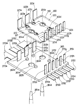
As shown in FIG. 16, a conductive portion device 300
is attached to an attaching base member 360.
3'1
CA 02228152 1998-O1-28
The attaching base member 360 is made of synthetic resin
and is of plate-like shape. Nine connecting members (the
first to the ninth connecting members 370A to 370I ) made of
metal are attached to the attaching base member 360 so as
to be embedded therein. The tip ends of the respective
connecting members 370A to 370I are connection ends 370a to
370i, which protrude on the surface side of the attaching
base member 360 at right angles.
Four positioning protrusions 362a to 362d are formed
at the attaching base member 360. The respective protrusions
362a to 362d are of substantially column-like shape.
Furthermore, the shape of the respective protrusions 362a
to 362d is not limited to the column-like shape. For example,
the shape may besubstantially conical, semi-spherical, etc.
Two holes 364a and 364b are formed on the attaching
base member 360. These holes 364a and 364b are formed in
correspondence to bosses 384a and 384b (described later).
The conductive portion device 300 is formed by adhering
three conductive materials(conductive portions) consisting
of a first conductive material 321, a second conductive
material 322 and a third conductive material 323, to the rear
side of the film 310.
The respective conductive materials 321 to 323 are made
32
CA 02228152 1998-O1-28
of metal having conductivity and are like a band having a
narrow width with each of the end sides branched into two
to be bifurcated, and each of both ends is folded at right
angles, thereby forming the connection ends 321a, 321d, 321e,
322b, 322f, 322g, 323c, 323h and 323i. The respective
connection ends 321a, 321d, 321e, 322b, 322f, 322g, 323c,
323h and 3231 correspond to the respective connection ends
370a to 3701 of the attaching base member 360.
Accordingly, holes 302a to 302d are formed at the
conductive portion device 300. Furthermore, preparatory
holes 304a and 304b are also formed at the conductive portion
device 300.
The respective holes 302a to 302d are formed to
correspond to the respective protrusions 362a to 362d of the
attaching base member 360. That is, the positions of the
respective holes 302a to 302d correspond to ( are coincident
with) the position of the protrusions 362a to 362d of the
attaching base member 360. Furthermore, the shape of the
respective holes 302a to 302d is substantially the same as
the cross-sectional shape of the protrusions 362a to 362d
of the attaching base member 360, that is, the shape of the
holes 302a to 302d and the cross section of the protrusions
362a to 362d are substantially circular, and the size of the
33
CA 02228152 1998-O1-28
respective holes 302a to 302d are substantially the same as
the size of the cross section of the protrusions 362a to 362d
of the attaching base member 360.
As shown in FIG. 2 0, the hole 302a is formed of a cutout
part 331a formed at the first conductive material 321 and
a cutout part 332a formed at the second conductive material
322. In other words, it can be said that the hole 302a is
formed of the three elements consisting of both the cutout
parts 331a and 332a, and a hole 316a of the film 310.
Similarly, the hole 302b is formed of a cutout part
331b of the first conductive material 321 and a cutout part
332b of the second conductive material 322 ( and a hole 316b
of the film 310 ) . The hole 302c is formed of a cutout part
332c of the second conductive material 322 and a cutout part
333c of the third conductive material 323 (and a hole 316c
of the film 310 ) . The hole 302d is formed of a cutout part
332d of the second conductive material 322, a cutout part
333d of the third conductive material 323 (and a hole 316d
of the film 310 ) .
Furthermore, the preparatory holes 304a and 304b are
formed so as to correspond to the respective holes 364a and
364b of the attaching base member 360. The hole 304a is
formed of a cutout part 341a of the first conductive material
34
CA 02228152 1998-O1-28
321 and a cutout part 342a of the second conductive material
322 ( see FIG. 17 ) ( and a hole 318a of the film 310 ( see FIG.
18)). Similarly, the hole 304b is formed of a cutout part
342b of the second conductive material 322 and a cutout part
343b of the third conductive material 323 (and a hole 318b
of the film 310 ) .
Next, returning to FIG. 16, a description is given of
a method of using this conductive portion device 300 and
peculiar operations and effects thereof.
Firstly, the attaching base member 360 is set at an
appointed position. At this time, the attaching base member
360 is set at an appointed position so that each of the bosses
384a and 384b is fitted into the respective holes 364a and
364b of the attaching base member 360. Both the bosses 384a
and 384b are made erect at appointed positions and are used
for positioning the attaching base member 360 and
preparatorily positioning the conductive portion device 300
with respect to the attaching base member 360.
Next, each of the bosses 384a and 384b is caused to
pass through the preparatorily positioning holes 304a and
304b of the conductive portion device 300, so that the
conductive portion device 300 is roughly positioned
preparatorily with respect to the attaching base member 360.
CA 02228152 1998-O1-28
Thereafter, the respective protrusions 362a to 362d of the
attaching base member 360 are caused to be fitted into the
holes 302a to 302d of the conductive portion device 300,
thereby positioning the conductive portion device 300 with
respect to the attaching base member 360.
Thus, it is possible to attach the conductive device
300 at an appointed position with respect to the attaching
base member 360 . Therefore , the respective connection ends
321a, 322b, 323c, 321d, 321e, 322f, 3228, 323h and 3231 can
be accurately brought into contact with the respective
connection ends 370a to 370i of the attaching base member
360.
Furthermore, since the positioning protrusions 362a
and 362b are located between the first conductive material
321 and the second conductive material 322, it is possible
to shirk that the first conductive material 321 and the second
conductive material 322 are brought into contact with each
other due to a certain reason, and the first conductive
material 321 can be prevented from being short-circuited to
the second conductive material 322. Furthermore, since a
plurality of positioning protrusions (362a and 362b) are
located between the first conductive material 321 and the
second conductive material 322, it is possible to further
36
CA 02228152 1998-O1-28
securely prevent them from being short-circuited, in
comparison with a case where the number of protrusion is
single. That is, in a case where any one or both of the
conductive materials ( 321 and 322 ) causes a positional slip
due to a certain reason, which turns so as to shirk the
corresponding single positioning protrusion, there is a
possibility that both the conductive materials 321 and 322
may be brought into contact with each other. However, in a
case where the number of the protrusions is plural, such a
possibility can be avoided. Furthermore, similarly; it is
possible to prevent the second conductive material 322 and
the third conductive material 323from being short-circuited
by the positioning protrusions 362c and 362d.
Furthermore, when attaching to another device the
assembly which is comprised of the attaching base member 360
and the conductive portion device 300 , by passing the bosses
which are similar to the bosses 484a and 484b and which are
formed at the another device through the holes 364a and 364b
of the attaching base member 360 and the holes 304a and 304b
of the conductive portion device 300, the assembly itself
can be easily attached to the another device at an appointed
position.
Next, a description is given of the method for
37
CA 02228152 1998-O1-28
manufacturing the conductive portion device 300.
A sheet-like metallic plate (see FIG. 17) and a
sheet-like film ( see FIG. 18 ) are prepared, and an adhesive
agent is coated onto the rear side of the film.
As shown in FIG. 17 , a coupled conductive material 332
is produced by die-cutting the metallic plate. The coupled
conductive material 332 is shaped so that three conductive
materials ( conductive portions ) 321 , 322 and 323 are coupled
to each other by coupling parts 334a to 334d. Cutout parts
341a, 342a, 342b and 343b are formed at the coupled conductive
material 332.Furthermore, connection ends 321a, 322b, 323c,
321d, 321e, 322f, 3228, 323h and 3231 are formed on the
coupled conductive material 332.
On the other hand, as shown in FIG. 18, holes 316a to
316d, and holes 318a and 318b are formed at the film 310 by
die-cutting the film 310.
Next, as shown in FIG. 19, the coupled conductive
material 332 is attached to the rear side of the film 310
(hereinafter called film-attached coupled conductive
material 340).
Next, as shown in FIG. 20, the coupling parts 334a to
334d are eliminated on the film-attached coupled conductive
material 340 by punching with a punching machine, and
38
CA 02228152 1998-O1-28
simultaneously, the cutout parts 331a and 331b of the first
conductive material 321, the cutout parts 332a to 332d of
the second conductive material 322 , and the cutout parts 333c
and 333d of the third conductive material 323 are formed.
At this time, the punching is carried out through the holes
316a to 316d of the film 310. Therefore, only the coupling
parts 334a to 334d of the coupled conductive material 332
can be eliminated without punching on the film 310. Thus,
three conductive materials consisting of the first to the
third conductive materials 321 , 322 and 323 are formed from
the coupled conductive material 332.
As described above, the conductive portion device 300
shown in FIG. 16 can be produced.
Accordingly, with this manufacturing method, it is
possible to obtain the effects as those of the first preferred
embodiment.
Furthermore, with this manufacturing method, by a
process of eliminating the caupling parts 334a to 334d of
the coupled conductive material 332 , the holes 302a to 302d
can be made simultaneously. Therefore, this is more efficient
than performing both the processes separately.
[Embodiment 5]
Next, a fifth preferred embodiment which is a
39
CA 02228152 1998-O1-28
modification example of the fourth preferred embodiment is
described on the basis of FIG. 21, centering around the points
which are different from the fourth preferred embodiment.
A conductive portion device 400 can be attached to an
attaching base member 460.
The attaching base member 460 is made of synthetic resin
and is of sheet-like shape. Nine connecting members (first
to ninth connecting members 470A to 470I ) made of metal are
attached so as to be embedded in the attaching base member
460.
Seven positioning protrusions 462a to 462g are formed
at the attaching base member 460. The positioning protrusions
462a and 462d are substantially of square-prism shape. The
positioning protrusions 462b, 462c, 462f and 462g are
substantially of triangular-prism shape. The positioning
protrusion 462e is substantially of circular-column shape.
The conductive portion device 400 may be formed by
attaching the three conductive materials (conductive
portions ) consisting of a first conductive material 421, a
second conductive material 422 and a third conductive
material 423 adhered onto the rear side of the film 410.
Positioning holes 402a to 4028 are formed on the
conductive portion device 400. Each of the holes 402a to 402g
CA 02228152 1998-O1-28
is formed so as to correspond to the respective protrusions
362a to 362g of the attaching base member 460 . That is , the
positions of the respective holes 302a to 302g correspond
to (are coincident with) the positions of the respective
protrusions 462a to 462g of the attaching base member 460.
Furthermore, the shape and size of the respective holes 402a
to 402g are substantially the same as the shape and size of
the cross section of the respective positioning protrusions
462a to 4628.
Furthermore, since the holes 402a and 402b are located
at points where the film 410 and the first conductive material
421 overlaps to each other, they may be formed of holes formed
at both the film 410 and the first conductive material 421.
Since the holes 402c and 402e are located at points where
only the film 410 exists (that is, no conductive materials
421 to 423 exist), they are formed at the film 410. Since
the hole 402d is located at points where the film 410 and
the second conductive material 422 overlaps to each other,
the same is formed of a hole formed at both the film 410 and
the second conductive material 422. Since the holes 402f
and 4028 are located at points where only the third conductive
material 423 exists (that is, no film 410 exists), it is
formed of a hole formed at the third conductive material 423.
41
CA 02228152 1998-O1-28
As in the fourth preferred embodiment, it is possible
to attach the conductive portion device 400 at an appointed
position with the attaching base member 460 so that the
respective positioning protrusions of the conductive
portion device 400 are fitted into the holes 402a to 402g
of the conductive portion device 400.
Furthermore, in this preferred embodiment, although
seven sets of positioning protrusions 462a to 4628 and holes
402a to 402g are provided, all the sets are not necessarily
required. In other sets than a set of a column-like
positioning protrusion 462e and a circular hole 402e, if any
one of the sets is provided, the conductive portion device
400 can be located with respect to the attaching base member
460.
Furthermore, if two or more sets of the column-like
positioning protrusions 462e and circular hole 402e exists,
the conductive portion device 400 can be located with respect
to the attaching base member 460.
Furthermore , as described above , even in a case where
only one set of a triangular prism positioning protrusion
462c and a triangular hole 402c exists, the conductive
portion device 460 can be located with the attaching base
member 460. However, since the hole 402 is provided at only
42
CA 02228152 1998-O1-28
the film 410, it is necessary for the respective conductive
materials 421 to 423 to be accurately positioned with respect
to the film 410 in order to accurately locate the respective
conductive materials (the first conductive material 421 to
the third conductive material 423) with respect to the
attaching base member 460.
Furthermore, the invention is not limited to each of
the above-mentioned preferred embodiments, it is needless
to say that the invention can be carried out in various kinds
of variations and modifications on the basis of the knowledge
of those skilled in this field.
43