Note: Descriptions are shown in the official language in which they were submitted.
CA 02228213 1998-O1-27
WO 97/05596 PCT/CA95/00450
INTEGRATED ANALOG SOURCE DRIVER FOR ACZTVE MATRIX LIQUID CRYSTAL DISPLAY
Field of the Invention
This invention relates generally to active-matrix liquid crystal displays
(AMLCDs), and more particularly to an analog source driver integrated directly
on
an AMLCD.
Fackground of the Invention
l0
Silicon integrated circuits are well known in the art for driving LCDs. Prior
art drivers which are fabricated separately from the LCD may be manufactured
with
transistor characteristics which can be matched reasonably well, and
operational
amplifier type feedback circuitry can be used to reduce the gain and offset
variations
between channels.
It is also known in the prior art to incorporate drivers for AMLCDs directly
on the LCD glass. Integral drivers have been designed in an effort to
eliminate
expensive prior art separate driver integrated circuits (ICs) and unreliable
edge
2 o interconnections between the drivers and AMLCDs, thereby reducing overall
system
cost and size of the optical heads incorporating the AMLCDs.
However, it is not a simple matter to design such integrated drivers since it
is difficult to manufacture TFT operational amplifiers as the output stages
would be
required to consist of plural TFTs connected in series across the power rails.
It
would not be possible to prevent all of the series pairs of TFTs on such an
integrated
driver from conducting simultaneously. This would result in non-uniformity and
poor
performance in some cases would short circuit the power supply.
3 o There have been several approaches suggested in the prior art for the
design
of integrated TFT (Thin Film Transistor) gate drivers. A gate driver functions
basically as a shift register. Consequently, prior art integrated gate drivers
have been
designed using drain clocking circuitry for achieving low power dissipation in
NMOS
CA 02228213 1998-O1-27
WO 97/05596 PCT/CA95/00450
2
CdSe TFTs comparable to that normally associated with CMOS devices. One such
prior art driver is set forth in an article of Schleupen, K., et al. entitled
"An
Integrated 4-bit Gray-Scale Column Driver for TV AMLCDs", 1994 SID Digest ,
(Society for Information Display).
,
However, there has been less progress in the prior art toward a consensus on
the design of TFT source drivers for AMLCDs. Indeed, there are presently two
distinct approaches to the design of source drivers: digital and analog.
Existing
digital source drivers are known for providing multiple bit outputs (eg. a 4
bit digital
1o driver can be implemented using four large capacitors and 21 TFTs), which
are
sufficient for low amplitude resolution applications such as aircraft
instruments or
simple on/off checklist displays. Although digital drivers are expandable to a
larger
number of bits, the device size approximately doubles for each added bit. By
way
of contrast, a single analog driver can be designed which is suitable for any
size of
display. Such a design should utilize no resistors, should be capable of
implementation in NMOS enhancement mode and must be compatible with the active
matrix TFTs (ie. identical thickness of semiconductor material).
A source driver comprises three basic functional blocks: an input video
2 o multiplexer, a storage device, and an output drive stage. The input video
multiplexer
and storage device may be connected in series or may effectively be connected
in
parallel if a double buffered sample-and-hold (S/H) is provided.
In the parallel embodiment, two or more S/Hs per output line, requiring one
2 5 TFT per S/H, are addressed for writing on alternate lines and reading on
other Iines
in accordance with the display pixel format and the video input format. The
output
of the S/Hs are multiplexed onto one output driver by additional TFTs, one per
S/H,
requiring four TFTs for the minimum implementation.
3 o For the series embodiment, the input S/Hs are loaded in succession after
which the stored data is loaded broadside into another parallel S/H which
functions
as an analog register. The series embodiment reduces the device input
capacitance
CA 02228213 1998-O1-27
WO 97/05596 PCT/CA95/00450
3
and only requires two TFTs for the minimum implementation but reduces the
voltage
to the driver since the charge on the first S/H must also drive the second S/H
without
amplification. The second TFT' must be characterized by a low resistance for
transferring the charge in a short deadtime between switching since the first
row of
TFTs cannot be permitted to receive signal again until the transfer has been
completed. The capacitors in the series S/H topology need only be of
sufficient size
to provide drive current for the duration of one line since that is all the
storage time
that is needed. However, the presence of two series stages tends to increase
the
switching noise. The double-buffered S/H needs twice the capacitance since
data
loaded at the beginning of one line must be retained through the end of the
next line.
The design of the output drive stage must take into consideration a number of
criteria and limitations dictated by the requirements for integration with the
display.
An essential feature of the output driver stage is that it must provide
accurate output
for any load while remaining independent of TFT threshold voltage.
Digital and analog drivers have been proposed which use a capacitive output
drive. However, these prior art designs are non-scalable to different direct-
view
applications since the output capacitor must be much larger than the combined
2 o capacitance of the source line and pixel capacitance (with one line of
array TFT's on).
Therefore, these prior art source drivers are restricted to use with very
small displays
for either projection or helmet-size direct viewing.
Summary of the Invention
According to the present invention, an integrated analog source driver is
provided which may be implemented using a minimal number of TFTs and
capacitors
(14 NMOS TFTs and 3 capacitors in the preferred embodiment), and no resistors
or
other types of devices. The integrated analog source driver of the present
invention
3 o may be fabricated concurrently with the active matrix devices of a
display, without
requiring any additional process steps. The output impedance of the inventive
integrated analog source driver is low enough to drive a broad selection of
displays
CA 02228213 1998-O1-27
WO 97/05596 PCT/CA9~/00450
4
ranging from projection/helmet displays to workstation displays. _ According
to the
present invention, the driver characteristics are made independent of TFT
characteristics through the use of a novel circuit architecture.
The integrated analog source driver of the preferred embodiment has two S/H a
stages, one being connected to the true analog video signal containing
standard RGB
type information, etc., and the other being connected to the inverted analog
video
signal. Adjacent video lines are connected to opposite polarity video signals,
and are
switched after each line in such a way that the polarity of the video may be
made to
1o alternate in both row and column directions in the manner of a
checkerboard, to
minimize the DC signal component tending to dissociate the LCD fluid and
polarize
the alignment layer (although alternatives to the checkerboard polarity method
may
be utilized such as row inversion, column inversion, frame inversion, etc.).
This
alternation is further reversed every frame. The two S/H outputs per source
driver
are multiplexed onto the gate of a source follower TFT such that while one S/H
is
driving the output stage with the signal for the current line, the other S/H
is acquiring
the signal for the next line. The output stage is a source follower which
drives one
active matrix source line and is the top TFT in a totem pole output stage. The
bottom device of the totem pole is a reset TFT whose drain is also connected
to the
2 0 output source line. The source follower and reset TFTs are prevented from
conducting current at the same time by switching off the source follower
either by a
second gate or by removing its supply voltage while the reset TFT is
conducting.
An autozero circuit is connected to the output stage for cancelling the effect
2 5 of TFT threshold voltage on the output source follower TFT. The autozero
circuit
operates such that the output voltage is driven to the signal level and then
reset to the
most negative voltage after the active matrix is disabled (by driving all
matrix gates
to the inactive state). The source follower gate is then grounded and the
output
voltage at the source line is stored on a capacitor whose other terminal is
grounded.
3 o The voltage on this capacitor is reversed by grounding the opposite side
and this
voltage is then placed in series with the S/H capacitor which is currently
driving the
output. The output is reset again and then the S/H gate signal is connected in
series
CA 02228213 1998-O1-27
WO 97/05596 PCT/CA95/00450
with the autozero value in the capacitor. This combined signal is applied to
drive the
source follower for the next line. Autozeroing in this fashion counteracts the
offset
of the output source follower TFT so that variations in the threshold voltage
of the
TFT do not affect the output. Since the gain in a follower stage is slightly
less than
5 unity, regardless of TFT variations, no gain calibration is required.
Brief Introduction to the Drawing
A detailed description of the preferred embodiment is provided herein below
1 o with reference to the drawings, in which:
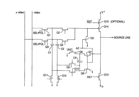
Figure 1 is a schematic diagram of an integrated analog source driver
according to the present invention; and
Figure 2 is a timing diagram showing sequence of operation of the elements
of the driver shown in Figure 1.
Detailed Descriution of the Preferred Embodiment
2 o The integrated analog source driver shown in Figure 1 uses a double-
buffered
input S/H (Q1, C1 and Q3, C2) driven by a shift register (not shown, but being
of
well lmown design). The shift register generates the Q1 and Q3 gating signals
shown
in Figure 2. When either one of the TFTs Q1 or Q3 is conducting, the
corresponding
one of the analog video signals (+ VIDEO, - VIDEO) is sampled via the
associated
2 5 storage capacitor C 1 or C2. However, in order to sample the signals onto
C 1 or C2,
TFTs Q11 or Q12, respectively, must be conducting so as to ground the lower
terminal of the capacitors. The double-buffered S/H outputs are multiplexed to
the
driver stage (Q14 and Q15) by two TFTs Q2 and Q4, in accordance with the
timing
signals for Q2 and Q4 as shown in Figure 2. A reset TFT Q13 is required to
reset
3 o the output signal in the presence of large pixel capacitance on the output
(SOURCE
LINE).
CA 02228213 1998-O1-27
WO 97/05596 PCT/CA95/00450
6
The stored charge on C 1 or C2 must have added to it a further charge equal
to the threshold voltage (V~ of the source follower Q14 to cancel the effects
of the
threshold voltage, and thereby eliminate threshold dependent non-uniformities
superimposed on the signal applied to the SOURCE LINE which would otherwise
occur. Therefore, as discussed in greater detail below, an autozero circuit is
incorporated for biasing capacitors C1 and C2 via series connected capacitor
C3 with
a sufficient charge to cancel the TFT threshold voltage (V~ of the source
follower
TFT Q14.
1o Thus, as shown in Figure 2, there are four operational phases per video
line.
First, the true (or inverted) video signal is applied to the SOURCE LINE
(denoted
as LINE O/P in Figure 2). The gates of the AMLCD TFT array switch on and off
in the usual manner for the duration of the LINE O/P, for generating the
required
video signal via the array pixel electrodes (not shown) which are connected to
the
SOURCE LINE.
Next, a first reset (denoted as RST in Figure 2) is performed, followed by the
aforementioned autozero function (AZ in Figure 2), and finally a second short
reset
(RST) is performed, as discussed in greater detail below.
25
The double-buffered input S/H design reduces insertion loss and input voltage
requirements, and permits line-by-line video inversion without extra
switching. Pixel-
by-pixel inversion is effected by driving the alternate S/~Is in the same row
by
antiphase video sources (+ VIDEO and - VIDEO). No external inversion is
required.
As indicated above, the driver stage comprises a source follower TFT (Q14),
shown in Figure 1 with an upper cascode gate (Q15) which is used for switching
,
only. As an alternative, two separate TFTs Q14 and Q15 may be used, or the V+
3 o supply may be gated externally without requiring TFT Q15. Also, as
discussed '
above, a reset TFT (Q13) is connected to the output (SOURCE LINE) to pull down
the output line voltage to a minimum voltage (V ) before and after autozero
capacitor
CA 02228213 1998-O1-27
WO 97/05596 PCT/CA95/00450
7
C3 is charged. The first and second resets occur during the "deadtime" between
LINE O/P phases, and must be able to discharge the SOURCE LINE capacitance
(typically several hundred pF). Since each pixel of the AMLCD is driven by a
video
signal of opposite polarity to the one above (or before) it, it is possible
for a
maximum signal voltage to be followed by a minimum voltage. Therefore, the
first
reset must be of sufficient duration to permit the SOURCE LINE capacitance to
be
discharged. The second reset (after autozero) is only half as long as the
first reset
since the SOURCE LINE voltage is below ground voltage after autozeroing. Since
the design includes no resistors, the capacitive load is reset to the negative
rail (V-),
1o and after RST signal is released, the source follower drives the output
(SOURCE
LINE) to the sampled signal level.
The autozero circuit shown in Figure 1 uses eight TFTs (Q5, Q6, Q7, Q8,
Q9, Q10, QlI and Q12) and one capacitor (C3). In operation, the driver input
is
grounded by switching TFT QS on with an autozero (AZ) signal. In response, the
output voltage (which is negative and approximately equal in magnitude to the
TFT
threshold voltage V~ is stored on capacitor C3 as a result of the AZ signal
also
switching TFTs Q7 and Q8 on while the unzero signal (UNZ) maintains TFT Q6 off
and logic low gate signals maintain TFTs Q9 and Q10 in the off state.
Accordingly,
2 o the polarity of the stored voltage is such that the capacitor plate
connected to Q6 and
Q7 is negative relative the plate connected to Q8, Q9 and Q10. Capacitor C3 is
then
electrically disconnected by switching off Q7 and Q8 (falling edge of AZ).
Capacitor
C3 is then electrically reconnected to the circuit by switching on TFT Q6
(rising edge
of UNZ) and one of either Q9 or Q10 (in Figure 2, Q9 is shown being switched
on).
2 5 The plate connected to Q6 and Q7 remains electrically negative relative to
the plate
connected to Q8, Q9 and Q10, but is electrically connected in such a way that
the
threshold voltage V~ is added rather than subtracted from the signal stored on
C 1 or
C2. Since the gain of the source follower is approximately unity, when voltage
is
inverted and placed on the gate of follower transistor Q14 by TFT Q6 and one
of
3o TFTs Q9 or Q10, it drives the output (SOURCE LINE) to zero volts regardless
of
the actual value of Vt.
CA 02228213 1998-O1-27
WO 97/05596 PCT/CA95/00450
8
As can be seen from Figure 2, the switching required to operate the driver of
the present invention is somewhat complex since the basic video S/H circuitry
requires four TFTs (Ql, Q2, Q3 and Q4) plus one transistor (QS) to ground the
gate ,
of source follower TFT Q14, and double-throw switching of the bottom terminals
of
S/H capacitors Cl and C2 between ground and the autozero capacitor C3 through
Q9,
Q10, Qll and Q12. Each side of the double buffer input must be connected
separately to the autozero capacitor C3 since when one of C1 or CZ is
connected to
the autozero capacitor C3 the other S/H capacitor must be grounded to store
the input
video signal. The TFTs (QS - Q12) and capacitor C3 used for autozeroing are
1 o preferably the same (small) size as the S/H TFTs and capacitors.
The total parts count of 14 (or 15) TFTs and 3 capacitors for implementing
the all-purpose analog driver of Figure 1 compares favourably with the 21 TFTs
and
8 capacitors used in the prior art 4-bit non-scalable switched-capacitor
driver
described in the article of Schleupen, K., et al., discussed above. It should
be noted
that this parts count does not include the TFTs used in the shift register
(not shown)
for addressing the S/H inputs nor the gates (not shown) used to generate the
Ql and
Q3 switching waveforms. Depending on the structure of the input S/H circuits
(there
may be more than two S/H circuits per channel), a S/H circuit fed by the video
signal
2 0 of either polarity must be activated for each input. Which input S/H
circuit is
activated depends on the polarity of the signal to be applied to the output.
In the
embodiment shown, either Q1 or Q3 would be selected. Accordingly, this may be
effected by using a pair of shift registers with output gating that selects
which one of
Ql or Q3 will be switched on. This selection logic would require the sampling
pulses
2 5 to be demultiplexed either at the shift register output or by the use of
cascode TFTs
a.~' ~Tlptlt CaTi'lplin~o l'~PViC'.PC~ ~e f~Trt~er is prefiar~~~o einnu
~.pi~,r' t ~L.e 1. an. '
va.uvav uuaw suuias at Lilt slillL reglJl.Gr
output does not degrade signal integrity whereas double-gate devices for Q1
and Q3
would likely inject extra switching noise. The shift register and the
additional
switching gates are not shown because they form part of the prior art, they
are
3 o ancillary to and do not form a part of the actual circuit of the invention
as set forth
in the claims below.
CA 02228213 1998-O1-27
WO 97/0596 PCT/CA95/00450
9
In summary, the integrated analog source driver of the_ present invention
overcomes the advantages of prior art p-Si and CdSe integrated source driver
designs
__ which use capacitive drives and which are only suitable for small displays,
by
providing a driver which is suitable as a "one-size-fits-all" solution for any
size of
display. It is believed to be hitherto unknown in the art to use autozeroing
as a
means of obtaining linear current amplification with independence from TFT
threshold characteristics. Furthermore, the driver is processed (ie.
fabricated)
concurrently with the array TFTs and therefore requires no new processes or
extra
processing steps and current amplification is provided. The small number of
circuit
1 o elements ~TFTs and capacitors - no resistors) allows the driver of the
present
invention to be made smaller than existing drivers for use with small pixel
pitches,
which is an important commercial consideration for high-resolution helmet and
projection display applications. The output impedance of the integrated driver
of the
present invention is sufficiently low to drive the source line capacitance of
a large
display panel, and the driver input impedance is high. The driver speed is
compatible
with video inputs. For wideband video, a plurality of separate inputs may be
provided to reduce bandwidth requirements. Also, video inversion may be
effected
in a straightforward manner
2 o Other embodiments and variations of the invention are possible For
example,
the input circuitry may be made according to a variety of designs to suit
different
input and pixel arrangements and polarity schemes. Also, the driver can be
fabricated
from a number of suitable semiconductor materials, such as amorphous silicon,
polycrystalline silicon, single-crystal silicon, gallium arsenide, germanium-
silicon as
2 5 well as cadmium selenide. All such alternative embodiments and variations
are
believed to be within the scope of the present invention having regard to the
claims
appended hereto.