Note: Descriptions are shown in the official language in which they were submitted.
CA 022282l4 l998-0l-27
W O 97/05654 PCT/CA95/00454
SEMICONDUCTOR SWITCH ARRAY WITH ELECTROSTATIC DISCHARGE
PROTECTION AND METHOD OF FABRICATING
TECHnNICAL FIELD
The present invention relates to a method of
protecting a semiconductor switch array from
electrostatic discharge damage and to a semiconductor
switch array incorporating electrostatic discharge
protection.
R~ JND ART
.Electrostatic discharge (ESD) damage is a well
known phenomenon and can occur during the fabrication of
semiconductor devices such as metal-oxide semiconductor
(MOS) structures. In structures of this nature, ESD
damage can result in gate insulating layer breakdown,
large shifts in threshold voltage and large leakage
currents between the gate and source electrodes or gate
and drain electrodes.
ESD damage is a more pronounced problem during
the fabrication of thin film transistor (TFT) switch
arrays for use in liquid crystal displays or in flat
panel detectors for radiation imaging. This is due to
the fact that the TFT switches are formed on an
insulating substrate (typically glass) and thus, the
source and drain electrodes may charge to a very high
voltage. Also, because peripheral circuits to which the
TFT switch array is to be connected are generally not
formed on the same sub~trate as the TFT switch array, the
gate and source lines must extend from the TFT switch
array sufficiently to allow the peripheral circuits to be
3 5 connected to the TFT switch array via wire bonding pads.
Any static charge picked up by the gate and source lines
is transferred to the gate and source electrodes of the
TFT switches as well as to the intersecting nodes of the
gate and source lines where the static charge is held.
CA 02228214 1998-01-27
W O 97/05654 PCT/CA95/00454
If the static charge reaches a high enough level, the
dielectric gate insulating layer between the gate and
source electrodes may breakdown. Even if this breakdown
can be avoided, the voltage differential between the gate
and source electrodes or gate and drain electrodes caused
by this held static charge may cause the threshold
voltage of the TFT switches to shift in either a positive
or negative direction.
Recently, a large amount of attention has been
given to the problems resulting from ESD damage
especially in active matrix liquid crystal displays and
flat panel detectors for radiation imaging. It is now
believed that ESD damage is also caused by equipment
related problems during the fabrication, handling and
testing of these types of devices. The trends to use
higher throughput equipment with higher speed substrate
h~n~ g as well as to downscale during the fabrication
process to reduce metal line width and reduce parasitic
capacitance in the TFT switches decrease ESD immunity.
one common ESD damage protection circuit used
with TFT switch arrays makes use of closed shorting bars
surrounding the TFT switch array to link all of the
source lines and the gate lines of the TFT switch array
together. The shorting bar associated with the gate
lines is formed at the time the gate lines are formed
while the shorting bar associated with the source lines
is formed at the time the source lines are formed. The
two shorting bars are electrically connected through vias
formed in the TFT switch array structure. Because the
shorting bars connect the gate and source electrodes of
all of the TFT switches in the array, the gate and source
electrodes remain at the same potential throughout the
fabrication process. This prevents any voltage
differentials from occurring across the gate and source
CA 02228214 1998-01-27
WO 97/05654 PCT/CA9S/00454
electrodes and therefore, inhibits ESD damage at these
electrodes.
Once the TFT switch array has been completely
fabricated, the shorting bars are removed by cutting off
u part of the glass substrate where the shorting bars
located. This cutting process is done before the
individual TFT switches are tested and before the gate
and source lines are connected to peripheral circuits.
Although the above ESD damage protection
circuit is widely used, once the shorting bars have been
removed, no ESD damage protection remains. This poses
problems since ESD damage often occurs during testing of
the TFT switches and during bonding of the gate and
source lines to peripheral equipment. This is in view of
the fact that at this stage, the TFT switch array is
handled by individuals and contacted with electronic
measuring equipment.
Another ESD damage protection network for TFT
switch arrays is disclosed in U.S. Patent No. 4,803,536.
This ESD damage protection network makes use of a strip
of N+ amorphous silicon resistive material film extending
to all of the bonding pads. The value of the resistive
material film is at least an order of magnitude greater
than the impedance of external driver circuits connected
to the bonding pads. By manipulating the resistance of
the resistive material film, static charges disperse to
all of the gate and source lines with an RC constant.
Although individual TFT switches can be tested without
removing the resistive material film, the resistive
material film crosses over all of the gate and source
lines. This causes crosstalk and electronic noise which
in certain applications, such as x-ray imaging where
signal currents are small, are serious problems.
CA 02228214 1998-01-27
W O 97/05654 PCT/CA95/00454
U.S. Patent No. 5,313,319 discloses yet another
ESD protection circuit for a TFT switch array. This
protection circuit includes static protection capacitors
formed on the substrate of the TFT switch array between
the gate and source lines. The thickness of the static
protection capacitors are chosen to ensure that they
breakdown due to static charges before ESD damage to the
TFT switches occurs. Unfortunately, the static
protection capacitors increase stray capacitance in the
TFT switch array thereby increasing electronic noise
making the TFT switch array unsuitable for many
applications.
Japanese Patent Nos. JPA2-61618, JPA62-198826
and JPAl-303416 and U.S. Patent No. 5,371,351 disclose an
ESD protection circuit for a TFT switch array which makes
use of photodiodes formed of an a-Si film. The
photodiodes connect the gate lines with the source lines
to minimize any potential voltage difference between
them. When the photodiodes are illuminated, the
resistance of the protection circuit decreases
dramatically creating short circuits between the gate and
source lines. When testing individual TFT switches, or
when operating the TFT switch array in normal conditions,
no incident light is permitted to impinge on the
photodiodes. This keeps the resistance of the protection
circuit very high to minimize crosstalk and leakage
currents.
U.S. Patent No. 5,220,443 discloses an ESD
protection circuit for a TFT switch array. The
protection circuit includes a common electrode
interconnecting the gate and source lines. Non-linear
resistive elements having a resistance that decreases
with an increase in voltage are connected between the
gate and source lines. The non-linear resistive elements
are realized using two back to back thin film diodes.
CA 02228214 1998-01-27
W O 97/05654 . PCT/C A95/00454
Because the resistive elements provide a large resistance
between the gate and source lines, individual TFT
switches can be tested without cutting the glass
substrate. Even after cutting the glass substrate, some
of the non-linear resistive elements remain to improve
- the ;~lln;ty of the TFT switch array to ESD damage.
However, the immunity of the TFT switch array to ESD
damage after cutting is significantly less than before
cutting.
The prior art ESD protection circuits referred
to above all have some common drawbacks. Firstly, none
of the ESD protection circuits protect the TFT switch
array from the first manufacturing stage (usually gate
line formation) to the last manufacturing stage (usually
wire bonding). During the manufacture of TFT switch
arrays for liquid crystal displays, it has been found
that ESD damage may occur during the process of spin
coating or stripping photoresist, during the cleaning
process using DI water, and during plasma etching. These
processes are often performed prior to the completion of
the TFT switch array structure. Isolating the gate lines
before f;n;sh;ng source line metallization as suggested
in the prior art may result in the build up of
electrostatic charge on the gate lines. Electrostatic
charges on the gate lines may become buried under the
dielectric film forming the gate insulating layer and
incubate until later stages in the manufacturing process.
During these later stages, the buried electrostatic
charges may move along the gate lines and concentrate at
a few points or boundary lines causing a breakdown in the
dielectric gate insulating layer.
In addition, in some instances since the gate
and source lines are interconnected by protection
elements, a failure in the connection between a gate or
source line and a protection element will result in the
CA 022282l4 l998-0l-27
W O 97/05654 PCT/CA951~0154
gate or source line being isolated from the common
electrode.
In the case of U.S. Patent No. 5,220,443,
although some ESD damage protection circuitry remains on
the substrate during the wire bonding process, the
impedance between an arbitrary gate line and a source
line may become too large to discharge electrostatic
charge quickly enough to avoid ESD damage. Accordingly,
better protection against ESD damage is desired.
It is therefore an object of the present
invention to provide a reliable method of protecting a
semiconductor switch array from ESD damage and a
semiconductor switch array incorporating electrostatic
discharge protection which obviates or mitigates at least
one of the above-described disadvantages.
8UMMaRY OF ~HE ll!lVI:~. lON
According to one aspect of the present
invention there is provided a method of inhibiting
electrostatic discharge damage to an array of
semiconductor switches formed on a common substrate and
arranged in rows and columns, individual ones of one of
the rows or columns of said array being interconnected by
source lines and the individual ones of the other of the
rows or columns of said array being interconnected by
gate lines, said method comprising the steps of:
during formation of said gate lines, connecting
one end of each gate line directly to a shorting element
and another end of each gate line to a shorting element
via a protection element;
during formation of said source lines,
connecting one end of each source line directly to a
shorting element and connecting another end of each
CA 02228214 1998-01-27
W O 97/05654 PCT/CA95/00454
source line to a shorting element via a protection
element; and
electrically coupling said shorting elements.
,~ .
According to yet another aspect of the present
~ invention there is provided a semiconductor switch array
incorporating electrostatic discharge protection
comprising:
an array of semiconductor switches formed on a
10 common substrate and arranged in rows and columns, the
individual ones of one of the rows or columns of said
array being interconnected by source lines and the
individual ones of the other of said rows or columns
being interconnected by gate lines; and
a pair of electrically coupled shorting
elements formed on said substrate, each of said gate and
source lines being connected to one of said shorting
elements directly and to one of said shorting elements
via a protection element.
In one embodiment, it is preferred that the
method further comprises the step of connecting the one
and another ends of each of the source lines to a first
shorting element, connecting the one ends of each of the
25 gate lines to a second shorting element and the another
ends of each of the gate lines to the first shorting
element electrically coupling the first and second
shorting elements.
In another embodiment, it is preferred that the
method further comprises the step of connecting the one
ends of the source and gate lines to a first shorting
element, connecting the another ends of the source and
gate lines to a second shorting element and electrically
coupling the first and second shorting elements. In this
case, it is also preferred that the one and another ends
of the source and gate lines alternate between opposite
CA 02228214 1998-01-27
WO 97/05654 PCT/CA95/00454
sides of the array. In both embodiments, it is preferred
that the protection elements are in the form of resistive
protection elements.
The present invention provides advantages in
that the ESD damage protection is maintained throughout
the entire manufacturing and testing process of the
semiconductor switch array and is fully compatible with
conventional semiconductor switch array fabrication
processes.
BRIEF DESCRIPTION OF THE DR~WINGS
Embodiments of the present invention will now
be described more fully with reference to the
accompanying drawings in which:
Figure 1 is a schematic of a flat panel
detector for radiation imaging incorporating a TFT switch
array;
Figure 2 is an equivalent circuit of a pixel
forming part of the flat panel detector illustrated in
Figure l;
Figure 3 is a schematic of a TFT switch array
incorporating an ESD damage protection circuit;
Figure 4 is a cross-sectional view of Figure 3;
Figure 5 is another cross-sectional view of
Figure 3;
Figure 6 is a schematic of an alternative
embodiment of a TFT switch array incorporating an ESD
damage protection circuit;
Figure 7 is a top plan view of a portion of the
TFT switch array illustrated in Figure 6;
Figure 8 is a top plan view of another portion
of the TFT switch array illustrated in Figure 6; and
Figure 9 is a cross-sectional view of Figure 7
taken along line 9-9.
-
CA 02228214 1998-01-27
WO 97/0S654 PCT/CA95/00454
BEST MODES FOR CARRYING OUT THE 1NV~11ON
Referring now to Figure 1, a flat panel
detector for radiation imaging is shown and is generally
indicated by reference numeral 20. The flat panel
detector includes a semiconductor switch array 21 in the
form of a plurality of pixels 22 arranged in rows and
columns. Gate lines 24 interconnect the pixels 22 of
each row while source lines 26 interconnect the pixels of
each column. The gate lines 24 lead to a gate driver
circuit 28 which provides pulses to the gate lines in
succession in response to input from a control circuit
29. The source lines 26 lead to charge amplifiers 30
which in turn are connected to an analog multiplexer 32.
The analog multiplexer provides image output which can be
digitized to create a digitized radiation image in
response to input from the control circuit 29.
Figure 2 shows an equivalent circuit of one of
the pixels 22. As can be seen, the pixel 22 includes a
radiation transducer CSE coupled to a storage capacitor CST
in the form of a pixel electrode 36. The pixel electrode
36 constitutes the drain electrode of a thin film
transistor ("TFT") switch 38. The source electrode of
TFT switch 38 is coupled to one of the source lines 26
while the gate electrode of the TFT switch is coupled to
one of the gate lines 24.
When the radiation transducer CSE is biased and
is exposed to radiation, it causes the pixel electrode to
store a charge proportional to the exposure of the
radiation transducer Cs~ to radiation. Once charged, the
charge can be read by supplying a gating pulse to the
gate terminal of TFT switch 38. When the TFT switch
receives the gate pulse, it connects the pixel electrode
36 to the source line 26 allowing the pixel electrode to
discharge. The charge on the source line 26 is detected
CA 02228214 1998-01-27
W O 97/05654 PCT/CA95/00454
by the charge amplifier 30 which in turn generates an
output voltage proportional to the detected charge. The
output voltage of the charge amplifier is conveyed to the
analog multiplexer 32.
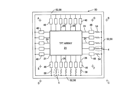
Referring now to Figure 3, during the
fabrication process, the array 21 of pixels 22 including
the gate and source lines 24 and 26 respectively are
fabricated on a common glass substrate. Wire bonding
pads 46 are formed at the ends of the source lines 26 for
testing or for wire bonding purposes. Similarly, wire
bonding pads 48 are formed at the ends of the gate lines
24. As mèntioned previously, during fabrication of the
TFT switch array 21, during its testing or when
connecting peripheral circuits to the TFT switch array 21
such as gate driver 28 and charge amplifiers 30, ESD
damage to the TFT switch array may occur. To reduce the
occurence of ESD damage during fabrication of the TFT
switch array 21, an ESD damage protection circuit 50 is
also fabricated on the glass substrate as will now be
described.
The ESD damage protection circuit 50 includes a
first shorting element in the form of a ring 52
~u~-oullding the TFT switch array and interconnecting all
of the gate lines 24 of the TFT switch array 21.
Specifically, the shorting ring 52 is connected directly
to the wire bonding pads 48 on one side of the TFT switch
array 21.
A second shorting element in the form of a ring
56 also surrounds the TFT switch array and interconnects
all of the source lines 26 of the TFT switch array 21.
The second shorting ring 56 is connected directly to the
wire bonding pads 46 on one side of the TFT switch array
21 and is connected to the wire bonding pads 46 on the
other side of the TFT switch array through resistive
CA 02228214 1998-01-27
WO 97/OS654 PCT/CA95/00454
protection elements 58. Shorting ring 56 is also
connected to each of the wire bonding pads 48 on the
other side of the TFT switch array 21 through a resistive
protection element 54. The two shorting rings 52 and 56
are electrically connected through vias (not shown)
formed in the TFT switch array structure. The resistive
protection elements 54, 58 provide current paths for
leaking electrostatic charges collected by the gate and
source lines 24 and 26 and have resistances at least one
order of magnitude greater than the impedance of the gate
and source lines.
Figures 4 and 5 best illustrate the resistive
protection elements 54 and 58 respectively. As can be
seen in Figure 4, resistive protection element 54
includes a Cadmium Selenide (CdSe) semiconductor material
c-h~n~el 78. Wire bonding pad 48 contacts the channel 78
through a via formed in the gate insulating layer 74 and
passivation layer 76. Shorting ring 56 also contacts the
channel 78. Resistive protection element 58 also
includes a CdSe channel 78 contacted by wire bonding pad
46 and shorting ring 56. Shorting ring 56 as mentioned
previously is connected to shorting ring 52 through vias
(not shown). The resistances of the resistive protection
elements 54 and 58 can be designed to change with bias
voltage in a linear or non-linear manner and may take the
form of one of a variety of structures such as for
example, TFT switches, TFD's (thin film diodes), zener
diodes or photodiodes.
As one of skill in the art will appreciate, the
shorting ring 52 is formed when the gate lines 24 are
being formed on the substrate of the TFT switch array
structure. The shorting ring 56 is formed when the
source lines 26 are being formed on the substrate.
CA 02228214 1998-01-27
WO 97/05654 PCT/CA95/00454
After the TFT switch array 21 and ESD damage
protection circuit 50 have been formed on the glass
substrate, the TFT switch array structure can be cut
along scribe lines ABCDA to expose the wire bonding pads
46 and 48 connected to the source and gate lines
ext~n~;ng from one side of the TFT switch array
permitting the individual TFT switches 38 in the array to
be tested. These scribe lines are marked so that part of
each shorting ring 52, 56 remains intact keeping the gate
and source lines 24 and 26 interconnected through the
resistive protection elements 54 and 58 during the
testing stage. If electrostatic charges appear on the
gate or source lines resulting in any unbalanced
potentials across the dielectric film constituting the
gate insulating layer of the TFT switch array, the
electrostatic charges will disperse quickly through the
resistive protection elements connected to the gate and
source lines.
Once testing has been completed, the outputs
from the gate driver 28 can be connected to the wire
bonding pads 48 of the exposed gate lines 24 via a wire
bonding process. Similarly, the inputs to the charge
amplifiers 30 can be connected to the wire bonding pads
46 of the exposed source lines 26 via a wire bonding
process. Thus, the TFT switch array 21 can be connected
to the peripheral circuitry with half of the ESD damage
protection circuit intact.
After the wire bonding processes have been
completed, the r~;n;ng half of the ESD damage
protection circuit 50 can be severed from the TFT switch
array 21 using a laser cutting operation made along
scribe lines EFG. However, the re~;ni~g half of the ESD
damage protection circuit may be useful when the flat
panel detector 20 is in operation by allowing gate pulses
applied to the gate lines to be fed back to the gate
CA 022282l4 l998-0l-27
W O 97/05654 PCT/CA9S/00454
13
driver 28 to shape the gate pulse waveform or to reduce
electronic noise. In addition, the remaining connections
between the resistive protection elements 54 and 58 and
the shorting rings 52 and 56 permits excess charge to
leak to ground, in the event that bond-wires peel off or
in the event that defects in the charge amplifiers 30 or
gate drivers 28 occur.
In some applications especially in high
resolution TFT liquid crystal displays and TFT flat panel
detectors, it is desired to use peripheral circuitry
connected to the gate and source lines on both sides of
the TFT switch array 21. Referring now to Figures 6 to
9, another embodiment of a TFT switch array 121
incorporating an ESD damage protection circuit 150 is
shown which is better suited to accommodate double-sided
peripheral circuitry. In this embodiment, like reference
numerals will be used to indicate like components with a
("100") added for clarity.
As can be seen, the ESD damage protection
circuit 150 includes a shorting ring 152 interconnecting
all of the gate lines 124 of the TFT switch array 121.
The shorting ring 152 is connected to only one end of
each gate line 124 through wire hon~; ng pads 148. The
connections between the shorting ring 152 and the wire
bonding pads 148 alternate between opposite sides of the
TFT switch array. Shorting ring 152 also interconnects
all of the source lines 126 of the TFT switch array
through vias formed in the TFT switch array structure.
The shorting ring 152 is connected to only one end of
each source line 126 through wire bonding pads 146. The
connections between the shorting ring 152 and the wire
bonding pads 146 also alternate between opposite sides of
the TFT switch array 121.
CA 02228214 1998-01-27
W 097/05654 PCT/CA95/00454
A second shorting ring 156 is connected to the
other end of each gate line 124 via resistive protection
elements 154. Shorting ring 156 is also connected to the
other end of each source line 126 via resistive
protection elements 158. The shorting rings 152 and 156
are electrically connected through vias 160 and 162
formed at the corners of the TFT switch array structure
(see Figures 7 and 8).
Figure 7 best illustrates one of the resistive
protection elements 154 although it should be realized
that both sets of resistive protection elements 154 and
158 are similar. As can be seen, resistive protection
element 154 includes a metal connection tab 170
contacting gate line 124 through vias 172 formed in the
gate insulating and passivation layers 174 and 176 of the
TFT switch array structure. The tab 170 contacts a CdSe
semiconductor material ~h~nnel 178. The shorting ring
156 also contacts the ch~n~el 178 but is spaced from the
connection tab 170.
After the TFT switch array 121 and ESD
protection circuit 150 have been formed on the glass
substrate, the TFT switch array can be cut along scribe
lines ABCDA to permit the individual TFT switches in the
TFT switch array to be tested. Similar to the previous
embodiment, the scribe lines are marked so that after
cutting, one end of each of the gate and source lines 124
and 126 r~ ~;n~ connected to shorting ring 156 via
resistive protection elements 154 and 158 respectively.
Once testing has been completed, the peripheral
circuits can be connected to the exposed wire bonding
pads 146 and 148 on opposite sides of the TFT switch
array 121. After this, the connections between the gate
and source lines and the shorting ring 156 can be severed
using a programmable laser cutting machine programmed to
CA 02228214 1998-01-27
W 0 97/05654 PCT/CA95tO0454
jump over the gate and source lines 124 and 126 connected
to peripheral circuits.
As one of skill in the art will appreciate, the
ESD damage protection circuits are present from the first
manufacturing stage of the TFT switch array (gate line
formation) right through to testing and connection of the
TFT switch array to peripheral circuits. Because of
this, the likelihood of ESD damage occurring to the TFT
switch array is reduced as compared to prior art switch
arrays.
Although the ESD damage protection circuits
have been described in conjunction with a TFT switch
array used in a flat panel detector for radiation
imaging, it should be apparent to those of skill in the
art that the ESD damage protection circuits can be
fabricated during the formation of TFT switch arrays for
other applications. Also, the ESD damage protection
circuits can be fabricated during the formation of other
semiconductor switch arrays where it is desired to
protect the switch array from ESD damage during its
formation and testing.
Those of skill in the art will also appreciate
that variations and modifications may be made to the
present invention without departing from the scope
thereof as defined by the appended claims.