Note: Descriptions are shown in the official language in which they were submitted.
CA 02228333 1998-01-29
THE~MOELECTRIC PRODUCT AND METHOD
FIELD OF THE INVENTION
This invention relates to cold junction compensators for use in thermoelectric,
thermocouple, or thermistor circuits, and in resistance - temperature circuits,
and to methods of use.
BACKGROUND OF THE INVENTION
In thermoelectric circuits it is necessary, for certain measurements, to utilise two
identical thermocouples and, whilst keeping one at a reference temperature, to
use the other to sense the temperature of an environment to be investigated.
Under laboratory conditions, the temperature of the first thermocouple is usually
maintainecl at ice point (zero degrees centigrade) by use of an ice bath, or at
some higher fixed temperature by means of a temperature-controlled oven, and
the first thermocouple is usually known as the reference or 'cold junction'. Tlle
other thermocouple is inserted in the environment under investigation and is
known as the 'sensing junction' or 'hot junction'. The known conventional
methods fi~r m~int~ining the first temperature-controlled junction at a constanttemperature are ~ti~f~ctory for use under laboratory conditions, but are
impractical in terms of weight, size, cost, power consumption, maintenance,
warm-up time and ice replacement or cont~min~tion, in many industrial
applications, and especially in aircraft and missile applications. The methods of
the present invention replace the above methods, as set out herein.
In particular, most practical constructions used hitherto have been of relatively
large size ,~d cumbersome in use because of the necessity to include a number
of separate items of equipment requiring interconnection with wiring between
those items, and also with wiring between the thermocouple junction itself and
the indication and/or recording equipment.
In the use of thermoelectric circuits it is desirable to have so-called'linearization'. This term describes the process by which an electrical circuit
converts the highly non linear curve of thermoelectric voltage versus
temperature to a linear curve of a device output voltage versus temperature.
CA 02228333 1998-01-29
Each calibration has in practice a unique non-linear calibration curve. By
providing linearization, the user does not need to use a table to relate a linear to
a non-linea~r curve, but can simply measure the output of the device and then
know that, for example, 1 milli-volt of output voltage is
equivalent to, say, 1 degree Centigrade or 1 degree Fahrenheit of measured
temperature.
Similarly in RTD (Resistance Temperature Detectors) and thermistors there is
need for correction. The output of an RTD is already linear for output versus
temperature, but the output curve is unique, and is offset. With this invention,the provision of linearization ensures that the user can measure the output of the
RTD and know that, say 1 milli-volt of output voltage, is equivalent to either 1degree Centigrade or 1 degree Fahrenheit of measured temperature.
Cold junction compensators for use with thermocouple circuits are disclosed in the
following documents:
US PATE~rr DOCUMENTS
1,205,325 11/1916 Clark ........... 136/222 X
1,228,678 6/1917 Johnson.......... 136/.222 X
1,411,033 3/1922 Jensen........... 136/222X
3,22~,597 12/1965 Engelhard ....... 73/361
3,650,154 3/1972 Arnett et al .... 73/361
3,916,691 11/1975 Hollander et al.. 73/361
4,133,700 1/1979 Hollander et al
FOREIGN PATENT DOCUMENTS
691809 8/1964 Canada .......... 73/361
OTHER PUBLICATIONS
Product Bulletin 803-A, Omega Engineering. Inc., 4 pages. Catalog No. C021 .
Consolidated Omega Devices. Inc., 6 pages.
Avasthy, 'Cold Junction compensation for Thermocouple Sensors' Jul. 1973,
CA 02228333 1998-01-29
pp 21 l to 2 ] 2, Institution of Engineers (India), vol. 53, pt 6.
U.S. Patent No. 4133700 of Hollander et al discloses a cold junction
compensator which provides the electrical equivalent of an ice-bath reference
thermocouple at a selected temperature, for example zero degrees Centigrade. Input
connectors, for engagement with conventional thermocouple units, form
thermocouple junctions with conductors connected to a battery-operated
Wheatstone ~3ridge circuit adapted to supply an equal and opposite voltage output
compensatic,n for variations in the thermocouple junction output at
different ambient temperatures.
OBJECTS OF THE INVENTION
A main object of the present invention is to provide an apparatus to serve as a
thermocoup]e output -to - analog connector module of a compact and easily
handled nat lre.
Another object is to provide such a connector module in which cold junction
compensatic,n is provided
Yet another object is to provide such a connector module in which the voltage
output is linearly related to the thermocouple temperature reading.
Yet another object is to provide such a connector module in which the voltage
output can readily be related alternatively to degrees Centigrade and to degreesFahrenheit.
Yet another object is to provide such a connector tnodule in which all the
linearity. and cold junction compensation corrections are perfo~ned by a
microprocessor.
A still further object is to provide such a connector module which can be readily
prograrr~ned for any of the thermocouple types J, K, or T, as explained herein.
CA 0222X333 1998-01-29
It is a further object of the present invention to provide an improved
construction of cold junction compensator which is in the form of a relatively
small and compact module cont~inin{~ all of the components required for a
compensation circuit fully wired and including any necessary power supply, the
module being adapted, for example, to include connector means, such as a pair
of sockets, for rapid connection and disconnection of a thermoelectric device,
and having output provision for a meter and/or recorder.
A still further object of the invention is to provide such a module with included
circuitry for linearization of the voltage output of a device so as to be
proportional to the temperature being tested.
Yet another object of the invention is to provide such a module with means at
least to lower, and preferably to elimin~te entirely, any stray electromagnetic
induction 'noise' which may be picked up by input leads from the device being
used in conjunction with the module.
Still further objects of the invention are to provide methods for obtaining an
analog resu.ltant from an electrical output of a thermoelectric device, and for
obtaining a linearized analo~ resultant, and for providing for calibration of said
analog resultant in degrees Centigrade and in degrees Fahrenheit, and for
providing coldjunction compensation of said analog resultants.
Still further objects and advantages of the invention will be apparent from the
description which follows with reference to the accompanying drawings.
CA 02228333 1998-01-29
SUMMARY OF THE INVENTION
According to the present invention, a cold junction compensator device
comprises, on a support. input terminals for connection to leads of a
thermoelectlic (thermocouple, thermistor, RTD) device, a printed circuit board
carlying the electronic components required for cold junction compensation,
and for lineanzation where applicable, battery means for power supply to the
printed circuit components, and output terminals for application of leads to a
voltage measuring meter and/or a voltage recorder or to a display wl~ich may
show a temperature in degrees Centigrade or degrees Fahrenheit
The support may further carry any one or more of the following:
(i) means for shielding the input terminals from stray electromagnetic induction noise;
(ii) 'on-off' switching means for the device;
(iii) one or more potentiometers for calibration of the circuitry;
(iv) means for indicating, at the exterior, the status of the power supply battery
means;
(v) switch nneans for ch~n~ing the output of the device to read in degrees
Centigrade or degrees Fahrenheit.
The hand- held support may have one or more removable and replaceable cover
portions for easy access to the interior thereof.
The compensator may be included in a module having input sockets or input plugs
to coact with plugs or sockets of conventional thermocouple units. The compensator
and battery may be encapsulated, or an accessible switch may be included in the
battery circuit.
CA 02228333 1998-01-29
A compensator device with linearization according to this invention is
adapted to the management of thermoelectric components including - ceramic semi
conductors, thermocouples, silistors, thermistors, RTD's (resistance temperaturedetectors) and thyristors. Electric currents are converted to readouts in degrees of
temperature; and temperature can be selected to control electrical performance
of operating equipment.
The invention is adapted to temperature sensors for, measurement, compensation, and
control and to flow sensing, gas analysis, liquid level/viscosity sensing, infrared
measurement and microwave power management. It is used in linearized networks
and bridge circuits. It is useful for instrument calibration.
BRIEF DESCRIPTION OF THE DRAW~N~JS
In the drawi]lgs:
Figure 1 is a composite perspective view of a hand-held cold junction
compensator module, with its base and two cover portions shown separated,
together with a representative meter and/or voltage recording means;
Figure 2 is a block diagram of the circuit of the cold junction compensator
module;
Figure 3 is a circuit block diagram of a connector module;
Figure 4A is a plan view of the module, with cover removed;
Figure 4B is a plan view of a cover for the module;
Figure 4C is a transverse section of the module casing taken at a first position of
the casing;
Figure 4D is a transverse section of the module casing taken at a second
position of the casing;
CA 02228333 1998-01-29
Figure 4E is an underplan view of the module;
Figure 4F iS a central vertical lon~itudin~l section through the module casing,
Figure 4G is an underplan view ofthe module c~cin~;
Figure 4H is an end view from one end of the module casing;
Figure 4I is another end view of the module casing, with part omitted;
Figure 4J is an end view of the entire module casing;
Figure 4K shows plan7 end and side views of an insertable plug for connection
to the module;
Figure S is a perspective illustration of the module in use, in conjunction with a
thermocouple, and a read-out/recording ~ s;
Figure 6 is a perspective view of the module, seen from one side and one end;
Figure 7 is a perspective view of the module, seen from the other side and otherend;
Figure 8 is a perspective view of the module seen from the underside;
Figure 9 is a perspective view of parts of another embodiment of cold junction
compensator module, with the parts seen in separated condition;
Figures lOA, lOB, lOC and lOD are respective portions of a circuit schematic
of the module of Figure 9;
CA 02228333 1998-01-29
Figure 11 is a perspective view of a casing of the module equipped with an
encircling coloured strip of resilient material for sealing and identification
purposes, e.p. in a contrasting yellow colour.
DETAILED DESCRIPTION OF THE PREFERRED
EMBODIMENTS
Referring to f;gure 1 of the drawing, a cold junction compensator module
comprises a base lA, a first cover portion lB, and a second cover portion lC.
A volt, or other, meter and/or a recording device, is denoted by reference 2.
The cover portion lB can be secured in position on the base lA by two screws
3 which pass through holes 4 in the cover portion lB and engage threaded
bosses 5 of ithe base lA. The cover portion lC can be secured on the base lA
by any conventional means, for example by m~king a sliding fit on side wall
ribbing 6 whLich may be a~lJro~liately undercut.
The base lA has an encircling wall 7 which is cut away (not shown) at the
right-hand end in this figure to permit access of two differently-sized male plug
pins of a th.ermoelectric aevice to a~l)rol)liate female so.ckets 8 mounted on
respective terminal posts 9 secured on the base lA. Each female socket 8 is
surrounded by a respective ferrite sleeve 10 to provide shielding from stray
electromagnetic interference.
Within the base lA there is secured a printed circuit board 11 having
appropriate circuitry for a compensation and linearization circuit. Also on the
board there ]is provided means for mounting batteries 12 supplying power to the
circuitry. A 'battery status' indicator (L.E.D) 13 can ~e brought into use when
required by means of a battery status switch 14. A main on-off switch for the
circuitry is shown at 15. Potentiometers 16 allow for calibration of the circuitry.
A switch 17 permits ch~nging of the output of the module to read in terms of
degrees Centigrade or degrees Fahrenheit, as the case may be. Output terminals
18 can be connected by respective leads 19 to the meter or recording device 2.
CA 02228333 1998-01-29
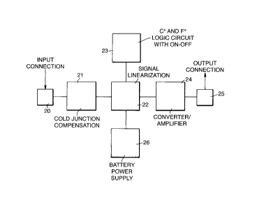
Figure 2 shows a block diagram of the cold ~unction compensator module. Input
connection 20 (corresponding to items 8, 9 and 10 of figure 1) has its output end
connected to the coldjunction compensation portion 21 of the printed circuit board.
The output of the compensation circuit is connected to the signal linearization
circuit 22 of the printed circuit board and the output therefrom can be varied to read
in terms of de,grees Centigrade or degrees Fahrenheit by operation of the logic
circuit 23. lrhe selected and linearized output passes to a converter/amplifier 24,
from which the output passes to output connection means 25 coupled to, for exarnple,
a voltmeter or voltage recording device (not shown). A battery supply 26, with on-off
switching and battery-status indicator, provides power.
As comparecl with previous encapsulated cold junction compensators, the present
invention has the following unique features and functions:
(i) It has the ability to linearize the thermoelectric output to a convenient 1 nnilli-volt
per degrele Centigrade or I milli-volt per degree Fahrenheit curve; also the output
signal can be calibrated to a specific unit of voltage or current per degree
CentigradLe or Fahrenheit and the linearized output signal is compatible with
instrumentation such as millivolt chart recorders, VOM, and other display
and recording devices.
(ii) It include s the use of ferrite cores to protect the thermoelectric input signals
from stray RFI radiation;
(iii) It includes a battery-life indicator which actuates automatically, as distinct from
requirinlJ the user to actuate a switch for that purpose;
(iv) It can be arranged to provide for 'Banana Plug' output connectors, as distinct
from screw terminals;
(v) Rubber gaskets may easily be included to make the device water resistant;
(vi) The inclusion of calibration potentiometers which are imrnediately
accessible to the user and can be used to check and adjust the calibration
CA 02228333 1998-01-29
in the field;
(vii) The module can be provided with a high input impedance, which:-
a) Allows for the use of thermocouples with high resistance while keeping the
signal loss to a minimum;
b) Perm~ts the use of thermocouples with long leads;
c) Permits the use of thermocouples made from fine gauge wire where speed
of response is desired.
Where there is a high input impedance, the input circuitry will be extremely
sensitive to RFI or EMI, and the built-in RFI or EMI suppression provides the
necessary protection.
(viii) The module can be provided with a low impedance output, and,-
a) With the output signal being kept close to ground potential there is less
chance of stray electromagnetic si~n~ls being induced into the signal leads;
b) A low impedance output will allow the signal to be transmitted over a
greater clistance with less chance of RFI or EMI.
(ix) The input and output can be balanced, which:-
a) Helps prevent ground loops;
b) Cuts down on interference affecting the input and output signal due to
cancellation of induced signals.
Referring IIOW to Figures 3 to 8, the apparatus shown in detail is a hand-held
thermocouple-to-analog connector module. It converts a thermocouple input
to a linear, compensated, analog output. The unit provides either lmV/Degreee
Fahrenheit or lmV/Degree Centigrade analog output. For example, if the
thermocouple input to the module is measu~ng 400 Degrees Fahrenheit
temperature, the unit provides 400 mV analog output.
The apparatus is microprocessor based. All the linearity and cold junction
compensation corrections are performed by a microprocessor The
CA 02228333 1998-01-29
microprocessor also interfaces with a key switch, and provides the functions of
the switch. It also performs all the logical functions and it drives all of a
plurality of LED' s on board. LED = light ernitting diode.
Figure 3 shows the circuit block diagram. The unit is powered by a 3 volts
lithium AA size battery. A switch interrupt circuit 101 interfaces with a key
switch and a microprocessor. This circuit controls the power to the rest of the
board. A charge pump circuit 102 converts the 3 volts input to +5.5 V and -
2.0V outputs. These voltages are used to power the rest of the circuit. A
voltage reference circuit 103 provides a stable and precise +5 volts output to the
rest of the board. A thermocouple amplifier circuit 107 amplifies the
thermocouple input to a high level signal. The high level signal goes through a
second stage of amplification and offset correction at amplifier 106. A
microprocessor 104 converts the output of the second stage amplifier 106 to a
digital signal. TC = thermocouple.
A thermocouple jumper selection 111 programs the microprocessor for any of
the three lypes of thermocouples J, K or T. Based on the thermocouple
selection, t]he microprocessor programs an analog switch 112 to set the gain andthe offset fi~r the corresponding thermocouple. The analog.switch also provides
the proper offset selection of an output amplifier 110 to switch between
lmV/degree Fahrenheit and lmV/degree Centigrade output.
TC = Thermocouple
J = Iron - constantan
K = C'hromel - alumel
T = Copper - constantan
There is a surface mount temperature sensor that measures the temperature of
the cold junction. The microprocessor takes the signal from the gain offset
arnplifier 106 and the temperature sensor 108 and by using the internal look-up
tables, it calculates the amount of correction the input signal needs and it
provides a pulse width modulation signal output. This signal goes through a
low pass filter circuit 9 to get converted to a DC signal. This DC signal is then
CA 02228333 1998-01-29
summarized with the output signal from the thermocouple amplifier 107 and the
temperature sensor 108. The output of the output arnplifier 110 provides a
linear, and compensated, analog signal output (1 mV/degree).
One unique ièature of this apparatus is that the microprocessor, which has a 4
channel, 8-biit analog to digital converter (AID) on board, only calculates
and provides the linearity correction necessary for the specific therrnocouple
at a specific temperature in the form of a pulse width modulation signal output.As a result, about 95% of the analog output comes directly from the output
of the thermocouple amplifier 107 and the temperature sensor 108 and only 5% of the
rem~ining signal comes from the microprocessor.
This arrange:ment is preferred over the conventional way of digitizing an analogsignal and providing a linearized signal output which is controlled by the
microprocessor completely.
The advantage of this arrangement is that the microprocessor is only providing
the linearity correction signal and as. a result it is possible to obtain the same
level of accuracy for the analog output with an 8-bit Al D versus a 10 or 12 bitAlD that controls the analog output completely.
The unit can be calibrated with a thermocouple simulator. In order to calibrate
the unit, three potentiometers have to be adjusted. P1 adjusts the temperature
span. P2 adjiusts the zero offset of the thermocouple. P3 adjusts for the degreeCentigrade offset. This allows proper conversion between mV/degree Fahrenheit
and mV/degree Centigrade analog output.
Figures 4A to 4J show the design concept of the c~sing The casing consists of two
plastic shells P, Q and a rubber gasket, R, which is sandwiched between the two
shells. This provides a water splash proof, sealed design. The case has 3 flex
fingers, S. T,he way the three finger areas are designed, makes these areas flexible.
With a graphic layer covering this area, and a momentary switch underneath the
flex finger, tlhis provides the membrane key action. The case also has 6 holes for
positioning I,ED'S, on the PC board. It also has a partition area, U, for adding
CA 02228333 1998-01-29
a liquid crystal display as an enhancement. The case incorporates a uni-connector,
V. This provides both an SMP and an OST thermocouple connection.
The lower shell Q provides a cradle for the AA size battery W. The top shell
also has a series of decorative grooves X, which give the case special style andlook. The two shells are assembled using mounting screws in holes Y.
The following is a s~mm~ry of the feature of a preferred embodiment of the
apparatus:
(a)A thermocouple to analog converter provides a linear compensated
ImV/degree Fahrenheit or Centigrade analog output;
(b) microprocessor based design;
(c) one button (key switch) operation;
(d) Off--- C)n (lmV/degree Centigrade) ------ On (lmV/degree Fahrenheit) -----
Off;
(e) The unit can be calibrated for three types of thermocouple inputs;
(f) J - from 100 to + 750 degree Centigrade;
(g) K - from -100 to + 1250 degree Centigrade;
(h) T - from -100 to + 350 de~ee Centigrade;
(i) There are three indicating LED's on board;
(j) 1 - Green LED for mV/degree Centigrade. It flashes once every 3 seconds in
normal operation.
2 - Green LED for mV/degree Fahrenheit. It flashes once every 3 seconds in
nonnal operation.
3 - Red ],ED for low battery indication. In normal operation, it is off. When
the battery voltage is low, it flashes once every second. When the battery
voltage gevts too low, the microprocessor shuts the p~wer off completely;
(k) If the. thermocouple input opens; the analog output can be driven upscale or downscale. At the same time the corresponding green LED flashes faster
(every sec).
(I) It operates from a single AA size 3 volts lithium battery. The battery should
last aboul: 3 months under continuous operation.
]4
CA 02228333 1998-01-29
(m) The PC board is designed to pass EMC requirements. The board is multi-
layer. The two internal layers are the ground plane and the power plane.
The two outside layers are the signal layers.
Referring to Figure 9, a base 201 has a cover 202 and the base and cover fit
together with a gasket 203. 204 is a modified uni-connector, and 205 is a PC
board which seats within the assembly of base and cover. Items 206 are
spacers. Items 207 are brass inserts which are used in the mechanical securing
together of the base and covers, by means of screws 208. Screw 209 engages
m a socket on base 202 to secure the uni-connector 204 in position. Screws
210 engage through openings in connector tabs of uni-connector 204, and
through openings in PC board 205, and are threaded into mounting pillars on
cover 202. A battery 211 can be engaged between connector clips on the PC
board 205. A screw 212 engages through an opening in the PC board 205 and
engages in a threaded mounting pillar 213 on the cover 202. 214 is a front labelfor the assembly, and 215 is a rear label, and 217 is a serial/model number
label.
Figures lOA, lOB, lOC, and lOD collectively show a circuit schematic of the
module of Figure 9.
Figure 11 is a perspective view of a modified form of casing for the module, thecasing 301 (shown empty of all other items of the module) having an encircling
sealing strip 302 of resilient material which is made of a distinctive colour, for
exarnple yellow, for the easy identification of the module.
The invention also provides a method for obt~inin~ an analog resultant from an
electrical output of a thermoelectric device which coIhprises steps of feeding
said electrical output to a linearization means, and feeding a linearized voltage
output from said linearization means to a display means. The method may
include the further step of converting said linearized output from said
linearization means selectively to a display of degrees Centigrade and to a
display of degrees Fahrenheit. There may be a still further step of calibrating
said linearized voltage output to a desired temperature scale.
CA 02228333 1998-01-29
The invention also provides a method for obtaining a coldjunction compensated
analog resultant from an electrical output of a therrnoelectric device, providing
coldjunction compensation of said electncal output, converting said cold-
junction compensated electrical output into a linearized output, and feeding said
output to a display.
16