Note: Descriptions are shown in the official language in which they were submitted.
CA 02228~38 1998-02-04
Field of the Invention
The invention relates to electrical testing probes and
lights for electrical testing probes.
Background of the Invention
Electrical testing probes are used to determine whether or
not a particular spot on a piece of equipment or wire is at a
voltage different from a given voltage. This is done by
attaching one end of the probe to a source of the given voltage
and touching the other end of the probe to the spot to be tested,
or using a pointed end of the probe to pierce a wire to be
tested. A small incandescent light bulb is electrically
connected between the two ends of the probe. If the voltage
difference across the light bulb is sufficient then current flows
through the bulb and the bulb lights. There are large numbers of
these types of probes in existence; mainly for use in automotive
testing. Obviously they are very limited in the testing
functions that they can perform.
Many improvements have been made to these simple probes.
For example, Sainz in US patent number 4,740,745 entitled
Polarity and Continuity Tester for Primary and Secondary
Automotive Circuits issued April 26, 1988 describes a probe with
a dual colour LED extending from one end of the probe. A voltage
drop across the probe in one direction causes the LED to
illuminate red and a voltage drop in the other direction across
the probe causes the LED to illuminate green. This allows the
user to check not only the existence of a voltage difference
CA 02228~38 1998-02-04
across the probe; but also, the polarity of the voltage
difference.
Mellott in US patent number 5,270,638 entitled Probe Device
for Testing Polarity of a Power Supply and Polarity of Test
Element with Respect to the Power Supply issued December 14, 1993
further describes a probe having a printed circuit board with two
dual colour LEDs inside of a transparent handle. The printed
circuit board fits into a custom cavity and is connected through
electrical clips to wires extending from the end of the cavity.
It is an object of the present invention to provide an
alternative probe and LED configuration.
Summary of the Inventlon
In a first aspect the invention provides a testing probe
having a prod, a handle, an end cap, a wire, a cavity, first and
second testing contacts, and a LED cartridge assembly. The prod
extends from the handle. The end cap encloses the cavity within
the handle and is removable from the handle to allow access to
the cavity. At least a portion of the handle is translucent
through to the cavity. The wire extends from the end cap outside
of the handle. The first and second testing contacts are in the
cavity and oppose one another. The first test contact is
electrically connected to the prod. The second test contact is
electrically connected to the wire. The LED cartridge assembly
has a first LED with a first anode and a first cathode and a
second LED with a second anode and a second cathode. Each LED
fits within a well in a holder. The first anode and second
CA 02228~38 1998-02-04
cathode are connected to a first assembly contact on a first end
of the holder and the first cathode and second anode are
connected to a second assembly contact on a second end of the
holder opposing the first end. A portion of the holder is
translucent to allow transmission of light from the first and
second LEDs through the holder. The holder is ~;mPncioned to fit
within the cavity of the probe with the first and second assembly
contacts in contact with, but not attached to, the first and
second testing contacts. The LED cartridge assembly is able to
be slipped into and out of the cavity when the end cap is removed
from the handle.
In a second aspect the invention provides an LED cartridge
assembly for use in a cavity of a testing probe between first and
second testing contacts. The testing probe has a prod, a handle,
an end cap, and a wire. The prod extends from the handle. The
end cap encloses the cavity within the handle. The end cap is
removable from the handle to allow access to the cavity. At
least a portion of the handle is translucent through to the
cavity. The wire extends from the end cap outside of the handle.
The first and second testing contacts are in the cavity and
oppose one another. The first test contact is electrically
connected to the prod. The second test contact is electrically
connected to the wire. The LED cartridge assembly has a first
LED with a first anode and a first cathode and a second LED with
a second anode and a second cathode. Each LED fits within a well
in a holder. The first anode and second cathode are connected to
a first assembly contact on a first end of the holder and the
first cathode and second anode are connected to a second assem~bly
contact on a second end of the holder opposing the first end. A
CA 02228~38 1998-02-04
portion of the holder is translucent to allow transmission of
light from the first and second LEDs through the holder. The
holder is dimensioned to fit within the cavity of the probe with
the first and second assembly contacts in contact with, but not
attached to, the first and second testing contacts. The holder,
first and second LEDs and first and second assembly contacts are
able to be slipped together into and out of the cavity when the
end cap is removed from the handle.
The LED cartridge assembly may have a spring for the first
assembly contact, and a button contact for the second assembly
contact. The holder may have first and second wells with the
first LED in the first well and the second LED in the second
well.
The holder may be generally cylindrical with a longitudinal
axis and opposing first and second holder ends along the
longitudinal axis. In this configuration, the first well extends
from the first holder end into the holder along the axis, the
second well extends from the second holder end into the holder
along the axis.
The respective anodes and cathode may be connected to one
another via leads extending from the first and second LEDs around
either side of the holder.
A first slot may be cut through the first well and the axis
from the first end toward the first LED. A second slot may be
cut through the second well and the axis from the second end
toward the second LED. In this configuration, the leads pass
CA 02228~38 1998-02-04
through the first and second slots and around the sides of the
holder.
The holder may have first and second opposing grooves
running longitudinally along either side of the holder with the
leads fitting into the grooves.
The second assembly contact may be a button contact
enclosing the second well at the second end of the holder. The
first assembly contact may be a spring extending along the axis
in the first well.
A protection resistor may be connected between the second
anode and the second assembly contact. Non-conductive electrical
insulation may be placed between the spring and the first
cathode. Non-conductive electrical insulation may be placed
between the resistor and the second cathode.
A conductive eyelet may be pressure fit into the second well
at the second end for receiving the second assembly contact. The
first LED may have a first colour and the second LED may have a
second colour visually distinguishable from the first colour.
The first and second LEDs may be in a single LED package in
a single well.
Brlef Descrlptlon of The Drawlngs
For a better understanding of the present invention and to
show more clearly how it may be carried into effect, reference
CA 02228~38 1998-02-04
will now be made, by way of example, to the accompanying drawings
which show the preferred embodiment of the present invention and
in which:
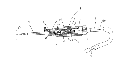
~igure 1 is a cross-section of a probe and LED cartridge
assembly according to the preferred embodiment of the
present invention,~igure 2 is a cross-section of the cartridge assembly of Figure
1,~igure 3 is a cross-section of portions of the cartridge
assembly of Figure 1 showing electrical connections,~igure 4 is an electrical diagram of the portions shown in
Figure 3,~igure 5 is a cross-section of a holder of the cartridge
assembly of Figure 1,
Figure 6 is a side view of the holder of Figure 5,
Figure 7 is an end view of the holder of Figure 5,~igure 8 is a cross-section of a prior art probe and bulb
assembly, and~igure 9 is a cross-section of a probe according to an alternate
preferred embodiment of the present invention.
Detalled Descrlptlon of the Drawlngs
Referring to Figure 1, a polarity testing probe 1 has a~andle 3. The handle 3 has a generally tubular cavity 5.
Extending from one end of the cavity 5 through the handle 3 is a~rod 7.
CA 02228~38 1998-02-04
Enclosing another opposing end of the cavity 5 is an end cap
9.
The end cap 9 may be pressure fit into the handle, as shown
in Figure 1. Alternatively, it may be screw fit or fit by some
alternative releasable means as would be evident to a person
skilled in the art.
A wire 11 extends from the end cap 9 outside the cavity 5.
There is an end cap contact 13 on the end cap 9 within the cavity
5. The contact 13 and the wire 11 are electrically connected.
On the opposing end of the wire 11 is a clamp 14 or other holding
device which would be evident to a person skilled in the art.
The prod 7 has a prod contact 15 opposing the contact 13
within the cavity. At an end of the prod 7, opposite the prod
contact 15, the prod 7 has a pointed tip 17. The prod 7 is
conductive from the tip 17 to the contact 15. Typically the prod
7 would be formed from metal. The tip 17 can be sharp enough,
and the prod 7 stiff enough, to pierce insulated electrical wire.
In an alternate embodiment, the tip 17 could be in alternate
shapes, such as a screw driver blade, not shown, for dual purpose
use; however, in such an application, the prod 7 would not be
able to pierce insulated wire for testing inside the wire.
In the preferred embodiment, the handle 3 is injected
moulded over the prod 7. The prod 7 has splines 18 to prevent
rotation or other movement between the handle 3 and prod 7.
CA 02228~38 1998-02-04
Alternatively, the prod 7 could be set into the handle after
moulding using a press fit with swages or other movement
resistant coupling, not shown, in place of the splines 18.
The end cap contact 13 and the prod contact 15 are opposing
test contacts 13, 15 within the cavity 5. Other opposing test
contacts could be used as would be evident to a person skilled in
the art, such as a button and folded spring combination as is
typically used in low voltage dry cell battery cavities, not
shown, or simply two opposing button contacts.
Within the cavity 5 between the contacts 13, 15 is a
cartridge assembly 19.
Referring to Figures 1 and 2, the cartridge assembly 19 has
two LEDS 21, 23 held by a holder 25. The holder 25 holds the
LEDS 21, 23 in place during manufacturing. The holder 25 also
provides support to the LEDS 21, 23 to prevent them, or their
leads, from contacting one another when the assembly 19 is placed
in the cavity 5. The leads of an LED are typically made from
aluminum and do not provide much support on their own. The
holder 25 also has other functions as will be evident from this
description to those skilled in the art.
The holder 25 and handle 3 are translucent and, preferably,
colourless. The holder 25 and handle 3 must allow the
transmission of light from the LED to the user of the probe in
such a way that the illumination of one LED 21, 23 is
distinguishable from the illumination of the other LED 23, 21,
CA 02228~38 1998-02-04
- 10 -
respectively. For the purpose~ of this description, transparent
materials are considered to be a subset of translucent materials.
The holder 25 and handle 3 are also non-electrically
conductive. The holder 25 is generally cylindrical and has an
axis 25b, which is generally aligned with the axis 25a.
Clear polycarbonate plastic has been found to be suitable
for both the handle 3 and holder 25. It is transparent and
transmits the light from the LEDs 21, 23 to outside the handle 3
with limited distortion, maintaining satisfactory brilliance,
particularly when combined with the latest ultra bright LEDs for
LEDs 21, 23.
Alternatively, acrylic or glass could be used for the handle
3 or holder 25, depending on the cost, temperature, ultraviolet,
and scratch and damage resistance properties and other propertieR
desired for the particular application.
Where the location of the LEDs is sufficiently
distinguishable by the user through the handle 3 and the holder
25, the LEDs need not be of different colour. Transparent handle
3 and holder 25 would be preferable in such an application. Even
though use of a single colour of LED is possible, different
colour LEDs 21, 23 are preferable for ease of use. The user need
only see the colour and does not have to closely examine the
probe 1 in order to determine which LED 21, 23 is illuminated.
The handle 3 and holder 25 do not have to be translucent
throughout there entirety. The handle 3 and holder 25 would be
CA 02228~38 1998-02-04
sufficiently translucent if translucent windows, not shown, were
provided through the handle 3 and holder 25 to the LEDs 21,23.
However, it is preferable for the holder 25 and handle 3 to be
translucent for 360 degrees about the longitudinal axis 25a of
the probe 1. It is also preferable for the handle 3 and holder
to be entirely translucent to permit light from the LEDs to pass
in all directions.
Referring to Figures 3 and 4, each LED has an anode 21a, 23a
and a cathode 21b, 23b. The anode 21a of one LED 21 i9 connected
to the cathode 23b of the other LED 23. The cathode 2lb of LED
21 is connected to the anode 23a of LED 23. The anode 21a is
also connected to a conductive spring 26 usually formed from
metal. A protection resistor 27 is connected to the other anode
23a. In low voltage DC application, for example the 6, 12 and 24
volts typically found in automotive applications, a 330 ohm, 1
watt resistor 27 has been found to be adequate. Other size
resistors can be used in other applications. Properly
configured, the probe can be used in all types of polarity
testing applications, for example computers, electronics and
aviation.
Referring to Figures 5 and 6, the holder 25 is generally
cylindrical. It has opposing wells 29, 31 drilled into opposing
ends of the holder 25. A slot 33, 35 is provided through an
outer portion 37, 39 of each well 29, 31.
Referring to Figures 5, 6 and 7, grooves 41, 43 are
provided on the exterior of the holder 25 between the slots 33,
35.
CA 02228~38 1998-02-04
- 12 -
Referring to Figure 2, LED 21 fits within well 29 and LED 23
fits within well 31. The wells 29, 31 may have a different
profile for LEDs having different package configurations. The
anode 21a is bent through slot 33 into groove 41. The cathode 23b
is bent through slot 35 into groove 41. Anode 21a and cathode 23b
are electrically connected together by soldering or other means
known in the art. Similarly, cathode 21b and anode 23a are
connected together along groove 43.
Spring 26 is soldered or connected to anode 2la in another
manner known in the art; 90 that, the spring 26 extends outwardly
from the LED 21 in the well 29. Similarly, the resistor 27 is
connected to the anode 23a and extends outwardly in the well 31.
Insulating washers 44a, 44b are placed between the spring 26
and cathode 21b and between the resistor 45 and cathode 23b,
respectively, to prevent shorting.
A tubular eyelet 45 with a flange 46 slips over the resistor
27 in the well 31. The well 31 is circular in cross-section and
closely receives the eyelet 45. The flange keeps the eyelet 45
from slipping completely into the well 31. The resistor 27 is
soldered or otherwise electrically connected to a solder button
47. The eyelet 45 simply acts as a receiving substrate for the
solder 47.
Referring to Figures 1 and 7, the well 29 is circular in
cross-section and ~;menRioned to allow the cartridge assembly 19
to closely fit over the prod contact 15 within the cavity 5. The
spring 26 comes into contact with the prod contact 15. The end
CA 02228~38 1998-02-04
cap 9 encloses the cavity 5 and the force of the spring 26
ensures that proper contact in maintained between the spring 26
and the prod contact 15 and between the end cap contact 13 and
the solder button 47. The solder button 47 and the spring 26 act
as cartridge assembly first and second contacts 47, 25,
respectively.
If one of the test contacts 13, 15 has a spring mechanism,
not shown, or the assembly 19 is closely matched to the ~;m~n~ion
between the test contacts 13, 15 in order to maintain proper
contact between the first contact 47 and the contact 13 and
between the second contact 25 and the contact 15 then the second
contact could be a button contact formed with an eyelet and
solder button, not shown, in place of the spring 26 in a manner
similar to the eyelet 45 and solder button 47.
In operation, the clamp 14 is attached to an acting ground,
for example the negative terminal of an automotive battery or an
exposed metallic portion of an automobile body, not shown. The
user grasps the handle 3 and touches a component to be tested.
If the component has a positive polarity with respect to the wire
11 then current flows through LED 21 and it illuminates. For the
preferred embodiment, LED 21 is red to indicate positive
polarity. If the component is negative with respect to the wire
11 then LED 23 will conduct and will illuminate. For the
preferred embodiment, LED 23 is green to indicate negative
polarity. As will be evident to those skilled in the art LEDs of
other colours could be used. Alternatively, the clamp can be
attached to a first wire in a circuit, not shown, and the prod 7
CA 02228~38 1998-02-04
touched to a second wire, not shown, in the circuit to determine
the relative polarity of the two wires.
If it is desired to replace the assembly 19, for repair or
replacement, the end cap 9 is simply removed and the cartridge is
slipped out of the cavity 5. Another assembly 19 can easily be
slipped into the cavity 5 and the end cap 9 is fit back into the
cavity. The used assembly 19 itself can be discarded or
defective components can be repaired if desired
Referring to Figure 8, the assembly 19 may be retrofit into
existing incandescent bulb probes 100. These probes 100
typically have a bulb assembly 102 with a bulb 103, bayonet mount
104 and a filament 105. The mount has an end contact 106 and
side contacts 108. The end contact 106 is insulated from the
side contacts 108. The side contacts 108 are connected to one
end of the filament 105 while the end contact 106 is connected to
the other end of the filament. A spring 110 fits over the bulb
opposite the end contact 106 until the spring 110 meets the side
contacts 108.
Other elements of the probe 100 are similar to the probe 1
and will not be re-described. Where the same reference numerals
are used below in describing components of the probe 100, the
components have the same functionality as the similarly numbered
component for the probe 100.
The assembly 102 is very simple to use. The clamp 14 is
attached to ground and the prod 7 is touched to a component to be
tested, not shown. If there is sufficient voltage difference
CA 02228~38 l998-02-04
- 15 -
between the prod 7 and the wire 11 then the bulb 103 will
illuminate. This simply indicates a voltage difference. It does
not indicate the polarity of that difference.
In order to upgrade the probe 100 to a probe 1, the assembly
102 is simply removed and replaced by an assembly 19. The
upgraded probe now has the ability to test for polarity.
The assembly 19 can also be use in other probes, not shown,
that have an internal cavity and opposing test contacts.
Referring to Figure 9, a probe 200 has an alternate
cartridge assembly 202 with two LEDs in a single package 204.
Each LED in the package 204 has a different colour. The package
2 04 replaces the LEDs 21, 2 3 and the anode and cathode of one of
the LEDs within the package 204 are connected to the cathode and
anode, respectively, of the other LED within the package 204. The
connection of the anodes and cathodes together may be internal to
the package 204 and first and second leads 206, 208 extend from
the package 204 as is shown in the preferred embodiment. One lead
206 i9 connected to the spring 26 and the other lead 208 i9
connected to the resistor 45. Alternatively, a lead for each
anode and cathode could extend from the package, not shown, and
the connections between anodes and cathodes would be external to
the package.
The package 204 fits in one of the wells 29, 31. Figure 9
shows the package 204 in well 29. The anode 206 fits through the
slot 33 and in the groove 41. The cathode 208 iS trimmed and
connected to the resistor 27.
CA 02228~38 l998-02-04
- 16 -
It i8 to be noted that the probes 1, 100 and 200 of the
preferred embodiment are identical except for the assemblies 19,
102, 202. This is a real advantage in manufacturing. An entire
line of probes 1, 100, 200 can be produced by reusing much of the
same tooling. Capital costs are reduced. Changing market
conditions, both in consumer demand and availability of supply,
can be more easily met by a manufacturer than with custom
configurations for each different probe 1, 100, 200.
Another advantage to the assemblies 19 and 202 of the
preferred embodiments is that they are not attached, by clips or
otherwise, to the remainder of the probes 1, 200. The assemblies
19, 202 simply slip in and out of the cavity 5. This feature
could be similarly achieved by having button contacts, not shown,
on both ends of the assemblies 19, 202 rather than a spring 26
and solder button 47. In this case it would be advantageous to
have a spring, or other resilient. contact, on either the prod
contact 15 or the end cap contact. 13 in order to provide lateral
pressure on each of the contacts 15, 13, 25, 47; however, if
tolerances are sufficiently accurate this may not be necessary
and simple button contacts could be used for each of the contacts
15, 13, 25, 47.
It will be understood by those skilled in the art that this
description is made with reference to the preferred embodiment
and that it is possible to make other embodiments employing the
principles of the invention which fall within its spirit and
scope as defined by the following claims.