Note: Descriptions are shown in the official language in which they were submitted.
CA 02228~71 1998-02-02
TITLE OF THE INVENTION
W~FER PROCESSING APPARATUS, WAFER PROCESSING METHOD,
AND SOI WAFER FABRICATION METHOD
BACKGROUND OF THE INVENTION
FIELD OF THE INVENTION
The present invention relates to a wafer processing
appa:ratus, a wafer processing method, and an SOI wafer
fabr:ication method and, more particularly, to a wafer
processing apparatus, a wafer processing method, and an
SOI wafer fabrication method which process a wafer by
dipping the wafer into a processing solution.
Wet etching is a typical example of processing
performed by dipping a wafer into a solution. One
subject of wet etching is to improve the in-plane
uniformity. Conventionally, the in-plane uniformity is
ensured by supplying fresh etching solution to the
react:ion surface by circulating the etching solution in
a bat:h.
Another example of the processing performed by
dipping a wafer into a solution is wafer cleaning
processing. Japanese Patent Laid-Open No.8-293478 has
disclosed a wafer cleaning apparatus which increases the
wafer cleaning efficiency by applying ultrasonic waves
CA 02228~71 1998-02-02
while vertically moving and rotating wafers contained in
a carrier cassette in a solution by a cam mechanism.
Another example of the wafer cleaning apparatus is
a ca,ssetteless wafer cleaning apparatus. A cassetteless
wafe:r cleaning apparatus is generally an apparatus in
whic]-L rod members are arranged parallel to each other,
grooves are formed in these rod members, and wafers are
clearLed while being supported by these grooves. In an
apparatus which cleans wafers contained in a carrier
cassette, portions of the wafers in the grooves of the
carrier cassette are difficult to clean. Also, since
most portions of the two sides of each wafer are covered
with constituent members of the carrier cassette, the
cleaning solution for wafers is mostly supplied from an
opening in the lower portion of the carrier cassette.
This tends to result in poor cleaning. A cassetteless
wafer cleaning apparatus is very effective to solve
these problems. Japanese Patent Laid-Open No.7-169731
has clisclosed a cassetteless wafer cleaning apparatus
capable of processing wafers of different sizes.
The wafer cleaning apparatus described in Japanese
Patent Laid-Open No.8-293478 cannot uniformly clean
wafers because the strength of ultrasonic waves is made
uneven by the constituent members of the carrier
casse!tte. In this wafer cleaning apparatus, the carrier
cassette is essential to prevent a fall of wafers when
CA 02228~71 1998-02-02
the wafers are rotated or vertically moved by the cam
mechcmism. The carrier cassette is commonly made from a
resin such as PFA or PEEK, but these materials do not
easi]y transmit ultrasonic waves. This decreases the
efficiency of the cleaning processing.
Also, the wafer cleaning apparatus described in
Japanese Patent Laid-Open No.7-169731 is very effective
to improve poor cleaning. However, the apparatus cannot
uniformly clean wafers because the wafers are cleaned
while being fixed in a bath. Additionally, since contact
portions between wafer support members and wafers are
fixed during cleaning, these contact portions are
difficult to clean.
SUMMARY OF THE INVENTION
The present invention has been made in
consideration of the above situation and has as its
object to make wafer processing uniform.
A wafer processing apparatus according to the
present invention is a wafer processing apparatus for
processing a wafer by dipping the wafer into a
processing solution, comprising a wafer processing bath,
and a rotary support mechanism for supporting a wafer
while rotating the wafer by a plurality of rod members
arranged substantially parallel to each other.
CA 02228~71 1998-02-02
The wafer processing apparatus preferably further
comp:rises ultrasonic generating means for generating
ultrasonic waves in the processing bath.
In the wafer processing apparatus, the rotary
support mechanism preferably applies a rotating force to
a wa:Eer by rotating at least a rod member, which
supports the wafer from a bottom surface side of the
processing bath, of the rod members.
In the wafer processing apparatus, the rotary
support member preferably applies a rotating force to a
wafer by rotating the rod members in the same direction.
In the wafer processing apparatus, each rod member
preferably has a groove for limiting movement of a wafer
in an axial direction.
In the wafer processing apparatus, the rotary
support mechanism preferably comprises driving force
generating means for generating a driving force for
rotating a wafer outside the processing bath.
In the wafer processing apparatus, the rotary
support mechanism preferably further comprises a crank
mechanism for transmitting the driving force generated
by the driving force generating means to the rod members.
The wafer processing apparatus preferably further
comprises a driving mechanism for rocking the rotary
support mechanism in the processing bath.
The wafer processing apparatus preferably further
CA 02228~71 1998-02-02
comprises a driving mechanism for floating or dipping
the rotary support mechanism.
In the wafer processing apparatus, the processing
bath preferably comprises a circulating mechanism
including an overflow bath.
In the wafer processing apparatus, the circulating
mechanism preferably comprises means for reducing
contamination of a wafer caused by particles which may
be produced by the rotary support mechanism.
In the wafer processing apparatus, the ultrasonic
generating means comprises an ultrasonic bath, an
ultrasonic source, and an adjusting mechanism for
adjusting a position of the ultrasonic source in the
ultrasonic bath, and ultrasonic waves are transmitted to
the processing bath via an ultrasonic transmitting
medium placed in the ultrasonic bath.
In the wafer processing apparatus, at least
portions of the processing bath and the rotary support
mechanism, which may come into contact with a processing
solution, are preferably made of a material selected
from the group consisting of quartz and plastic.
In the wafer processing apparatus, at least
portions of the processing bath and the rotary support
mechanism, which may come into contact with a processing
solution, are preferably made of a material selected
from the group consisting of a fluorine resin, vinyl
CA 02228~71 1998-02-02
chloride, polyethylene, polypropylene,
polybutyleneterephthalate (PBT), and
polyetheretherketone (PEEK).
In the wafer processing apparatus, the rotary
support mechanism preferably supports a wafer by four
rod members.
In the wafer processing apparatus, the rod members
are preferably arranged in a position where rotation of
a wafer having an orientation flat is not prevented by
the orientation flat when the wafer is processed.
A wafer processing apparatus according to the
present invention is a wafer processing apparatus for
processing a wafer by dipping the wafer into a
processing solution, comprising a wafer processing bath,
support means for supporting a wafer from both sides and
below by a rod member to hold the wafer substantially
perpendicular to a bottom surface of the processing bath,
and cLriving means for rotating the supported wafer.
The wafer processing apparatus preferably further
comprises ultrasonic generating means for generating
ultrasonic waves in the processing bath.
In the wafer processing apparatus, the driving
means preferably applies a rotating force to a wafer by
rotating the rod member.
In the wafer processing apparatus, the rod member
preferably has a groove for limiting movement of a wafer
CA 02228~71 1998-02-02
in an axial direction.
A wafer processing method according to the present
invention is a wafer processing method of processing a
wafer by dipping the wafer into a processing solution,
wherein a wafer is rotated while being supported from
two sides and below by a rod member, the wafer being
held substantially perpendicular to a bottom surface of
a processing bath.
In the wafer processing method, it is preferable
that while a wafer is rotated in the processing bath,
ultrasonic waves be generated in the processing solution.
The wafer processing method is suited to wafer
etch:ing by using an etching solution as the processing
solution.
The wafer processing method is suited to etching of
a wafer having a porous silicon layer by using an
etching solution as the processing solution.
An SOI wafer fabrication method according to the
present invention is an SOI wafer fabrication method of
fabricating an SOI wafer by using the wafer processing
method described above in a part of fabrication steps.
A wafer processing method according to the present
invention processes a wafer by using the wafer
processing apparatus described above.
A wafer processing method according to the present
invention etches a specific layer formed on a wafer by
CA 02228~71 1998-02-02
using the wafer processing apparatus described above.
An SOI wafer fabrication method according to the
present invention fabricates an SOI wafer by using the
wafer processing method described above in a part of
fabrication steps.
Further objects, features and advantages of the
present invention will become apparent from the
following detailed description of embodiments of the
present invention with reference to the accompanying
drawings.
BRIEF DESCRIPTION OF THE DRAWINGS
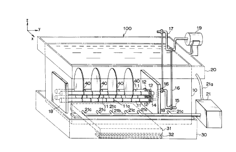
Fig. 1 is a perspective view showing an outline of
the construction of a wafer processing apparatus
according to a preferred embodiment of the present
invention;
Fig. 2 is a sectional view of the wafer processing
apparatus shown in Fig. 1;
Fig. 3 is a sectional shape showing the shape of a
wafer rotating rod;
Fig. 4 is a view showing an outline of the
construction of a wafer rotating mechanism;
Fig. 5 is a view showing an outline of the
construction of the wafer rotating mechanism;
Fig. 6 is a view schematically showing the
-- 8
CA 02228~71 1998-02-02
arrangement of a wafer processing system in which a
plurality of wafer processing apparatuses are arranged;
Fig. 7 is a view showing another example of the
construction of the wafer rotating mechanism;
Fig. 8 is a view showing an outline of the
construction of a wafer processing apparatus including
the wafer rotating mechanism shown in Fig.7; and
Figs.9A to 9F are sectional views showing the steps
of an SOI wafer fabrication method.
DETAILED DESCRIPTION OF THE PREFERRED EMBODIMENT
A preferred embodiment of the present invention
will be described below with reference to the
accompanying drawings. Fig.1 is a perspective view
showing an outline of the construction of a wafer
processing apparatus according to the preferred
embodiment of the present invention. Fig.2 is a
sectional view of the wafer processing apparatus shown
in Fig. 1.
In a wafer processing apparatus 100 according to
this embodiment, portions which may come into contact
with a processing solution are preferably made from
quartz or plastic in accordance with the intended use.
Preferable examples of the plastic are a fluorine resin,
vinyl chloride, polyethylene, polypropylene,
CA 02228~71 1998-02-02
polybutyleneterephthalate (PBT), and
polyetheretherketone ( PEEK). Preferable examples of the
fluorine resin are PVDF, PFA, and PTFE.
This wafer processing apparatus 100 has a wafer
processing bath 10, an overflow bath 20, an ultrasonic
bath 30, and a wafer rotating mechanism (11 to 19) for
supporting wafers 40 while rotating these wafers.
To process wafers, the wafer processing bath 10 is
filled with a processing solution (e.g., an etching
solution or a cleaning solution). The overflow bath 20
for temporarily storing any processing solution
overflowing from the wafer processing bath 10 is
provided around the upper portion of the wafer
processing bath 10. The processing solution temporarily
stored in the overflow bath 20 is discharged from the
bottom portion of the overflow bath 20 to a circulator
21 through a discharge pipe 21a. The circulator 21
removes particles by filtering the discharged processing
solution and supplies the processing solution to the
bottom portion of the wafer processing bath 10 through a -
supply pipe 21b. Consecluently, particles in the wafer
processing bath 10 are efficiently removed.
The wafer processing bath 10 preferably has a depth
by which the wafers 40 are completely dipped. This
prevents particles in the air and those gathering around
the upper portion of the wafer processing bath 10 from
- 10 -
CA 02228~71 1998-02-02
adhering to the wafers 40.
The ultrasonic bath 30 is arranged below the wafer
processing bath 10. An ultrasonic source 31 is supported
by an adjusting mechanism 32 inside the ultrasonic bath
30. This adjusting mechanism 32 includes a mechanism for
adjusting the vertical position of the ultrasonic source
31 and a mechanism for adjusting the horizontal position
of the ultrasonic source 31, as mechanisms for adjusting
the relative positional relationship between the
ultrasonic source 31 and the wafer processing bath 10.
By this mechanism, ultrasonic waves to be supplied to
the wafer processing bath 10, more specifically, to the
wafers 40 can be optimized. The ultrasonic source 31
preferably has a function of adjusting the frequency or
strength of ultrasonic waves to be generated. This
further optimizes the supply of ultrasonic waves. Since
the apparatus thus has the function of optimizing the
supply of ultrasonic waves to the wafers 40, various
types of wafers can be processed. The ultrasonic bath 30
is filled with an ultrasonic transmitting medium (e.g.,
water), and this ultrasonic transmitting medium
transmits ultrasonic waves to the wafer processing bath
10 .
The wafers 40 are held to be nearly perpendicular
to the bottom surface of the wafer processing bath 10 by
four wafer rotating rods 11 having grooves lla for
CA 02228~71 1998-02-02
engaging with the wafers 40. These wafer rotating rods
11 have a function of supporting the wafers 40 while
rotating them and form a part of the wafer rotating
mechanism. The wafer rotating rods 11 are rotatably
supported by a pair of opposing rod support members 18
and rotated in the same direction by a driving torclue
generated by a motor 19. The wafer rotating rods 11
preferably have a small diameter by which the
transmission of ultrasonic waves is not prevented.
The number of wafer rotating rods 11 is preferably
as small as possible. To ensure the frictional force
with the wafers 40, however, it is preferable to use two
wafer rotating rods 11 for limiting the movement in the
rolling direction ~x-axis direction) of the wafers 40
and two wafer rotating rods 11 for supporting the wafers
40 from below. By arranging two appropriately spaced
wafer rotating rods 11 below wafers, the driving torclue
can be efficiently transmitted to wafers having
orientation flats. This is so because if only one wafer
rotating rod 11 is present below the wafer and the
orientation flat of the wafer is positioned on this
wafer rotatlng rod 11, the wafer cannot be rotated by
the wafer rotating rod 11.
Standing waves, i.e., high- and low-strength
portions of ultrasonic waves are usually formed between
the bottom surface of the wafer processing bath 10 and
- 12 -
CA 02228~71 1998-02-02
the liquid surface. In this wafer processing apparatus
100, however, the nonuniformity of the processing
resu:lting from standing waves is decreased because the
wafers 40 can be processed while being rotated.
This wafer processing apparatus 100 has a structure
in which members on the bottom portion of the wafer
processing bath 10 and around the wafers 40 are removed
as many as possible. Accordingly, the supply of
ultrasonic waves to the wafers 40 can be made efficient
and lmiform. Also, this structure allows the processing
solution near the wafers 40 to freely flow. This makes
the processing for the wafers uniform and prevents the
occurrence of a processing failure.
Fig. 3 is a sectional view showing the shape of the
wafer rotating rod 11. The wafer rotating rod 11 has a
plurality of grooves lla for supporting the beveling of
the wafer 40 by clamping it. The shape of the grooves
lla is preferably a U shape or a V shape. In this wafer
processing apparatus, no specific region of the beveling
of the wafer 40 is constantly supported because the
wafer rotating rod 11 supports the wafer 40 while
rotating it. Accordingly, the beveling of the wafer 40
can also be uniformly processed.
Figs. 4 and 5 are views showing an outline of the
construction of the wafer rotating mechanism. The four
wafer rotating rods 11 are arranged parallel to each
CA 02228~71 1998-02-02
other in the horizontal direction (y-axis direction) so
as to extend along a columnar shape formed by the wafers
40. A driving force transmission gear 12 is provided
near the end portion of each wafer rotating rod 11. A
driving torque generated by the motor 19 is transmitted
to a crank 15 via a crank 17 and a connecting rod 16. A
driving force transmission gear 14a is provided at the
end portion of the crank 15. The driving torque
transmitted to the driving force transmission gear 14a
is transmitted to the driving force transmission gears
12 via intermediate gears 14. By this arrangement, the
wafer rotating rods 11 rotate in the same direction at
the same speed.
In the embodiment shown in Figs.4 and 5, the
driving torque generated by the motor 19 is transmitted
to the crank 15 and distributed to the wafer rotating
rods 11 in order to simplify the construction. However,
cranks can also be provided in a one-to-one
correspondence with the wafer rotating rods 11. If this
is the case, it is unnecessary to provide the driving
force transmission gears 12 and 14a and the intermediate
gear 14. Consequently, the production of particles
resulting from the friction of the gears can be
prevented.
It is not always necessary to simultaneously rotate
the four wafer rotating rods 11. To efficiently transmit
- 14 -
CA 02228~71 1998-02-02
the rotating force to the wafers 40, however, it is
preferable to rotate at least one wafer rotating rod 11
below the wafers 40. Furthermore, to more efficiently
transmit the rotating force to the wafers 40 or to
smoothly rotate wafers having orientation flats, it is
preferable to rotate the two wafer rotating rods 11
below the wafers 40.
The wafer rotating mechanism is not restricted to
the above construction. That is, any mechanism can be
used as long as the mechanism can rotate the wafer
rotating rods 11 in the same direction. For example, it
is also possible to use a construction which transmits
the driving force of the motor 19 to the driving force
transmission gear 14a by a bevel gear or a belt.
In this wafer processing apparatus 100, supply
ports 21c for supplying the processing solution to the
wafer processing bath 10 are arranged near the bottom
portion of the wafer processing bath 10 so that the
processing solution circulates upward from the bottom
portion of the wafer processing bath 10. Furthermore, in
this wafer processing apparatus 10, a plurality of
supply ports 21c are arranged near the wafers 40 to
adjust the flowing direction of the processing solution,
so that the processing solution near the driving force
transmitting mechanism constituted by the gears 12, 14,
and 14a, the crank 15, the connecting rod 16, and the
CA 02228~71 1998-02-02
like does not move to the wafers 40. This reduces the
possibility of the wafers 40 being cont~m;n~ted by
particles that may be produced by the friction of the
driving force transmitting mechanism.
Some other means can also be used to prevent the
contamination of wafers by particles which may be
produced by the driving force transmitting mechanism.
For example, it is effective to adjust the diameter of
each supply port 21c or to form a partition for
separating the wafers 40 and the driving force
transmitting mechanism.
Fig. 6 is a view schematically showing the
arrangement of a wafer processing system in which a
plurality of wafer processing apparatuses are arranged.
Wafer processing apparatuses lOOa to lOOc have
essentially the same construction as the wafer
processing apparatus 100 described above. In this
embodiment, the apparatuses lOOa and lOOc are used as
cleaning apparatuses, and the apparatus lOOb is used as
an etching apparatus.
Each of single wafer transfer robots 60a to 60c
holds a wafer by vacuum-chucking the rear surface of the
wafer. Under the control of a computer, the transfer
robot 60a vacuum-chucks a wafer 40 completely processed
in the preceding step, transfers the wafer 40 to the
cleaning apparatus lOOa, and sets the wafer 40 so that
- 16 -
CA 02228~71 1998-02-02
the wafer fits in corresponding grooves lla of wafer
rotating rods 11 of the cleaning apparatus lOOa. When a
predetermined number of wafers 40 are set in a wafer
processing bath 10, the cleaning apparatus lOOa executes
cleaning processing while rotating the wafer rotating
rods 11 under the computer control.
When the cleaning apparatus lOOa completely cleans
the wafers 40, under the computer control the transfer
robot 60b vacuum-chucks the wafer 40 in the wafer
processing bath 10 of the cleaning apparatus lOOa,
transfers the wafer 40 to the etching apparatus lOOb as
the next wafer processing apparatus, and sets the wafer
40 so that the wafer fits in the corresponding grooves
lla of the wafer rotating rods 11. When a predetermined
number of wafers are set in the wafer processing bath 10,
the etching apparatus lOOb executes etching processing
while rotating the wafer rotating rods 11 under the
computer control.
When the etching apparatus lOc completely etches
the wafers 40, under the computer control the transfer
robot 60c vacuum-chucks the wafer 40 in the wafer
processing bath 10 of the etching apparatus lOOb,
transfers the wafer 40 to the cleaning apparatus lOOc as
the next wafer processing apparatus, and sets the wafer
40 so that the wafer fits in the corresponding grooves
lla of the wafer rotating rods 11. When a predetermined
CA 02228 j71 1998-02-02
number of wafers are set in the wafer processing bath 10,
the cleaning apparatus lOOc executes cleaning processing
while rotating the wafer rotating rods 11 under the
computer control.
Fig.7 shows another example of the construction of
the wafer rotating mechanism. This wafer rotating
mechanism 110 has a function of rocking wafer support
members in the wafer processing bath 10 and a function
of raising the wafer support members to a position above
the wafer processing bath 10, thereby enabling loading
and unloading of the wafers 40 outside the wafer
processing bath 10. The former function can make the
processing performed for the wafers 40 more uniform. The
latter function facilitates loading and unloading of the
wafers 40. With this function, it is also possible to
move wafers to another processing bath while the wafers
are set in the rotating mechanism.
In this wafer rotating mechanism 110, two rod
support members 18 and 18' are connected by connecting
members 51. The motor 19 is fixed to the rod support
member 18' rather than the overflow bath 20. An arm 52
for moving the wafer rotating mechanism 110 by a robot
is attached to the rod support member 18'.
Fig. 8 is a view showing an outline of the
arrangement of a wafer processing apparatus including
the wafer rotating mechanism 110. A robot 50 can sink
- 18 -
CA 02228~71 1998-02-02
and raise the wafer rotating mechanism 110 into and from
the wafer processing bath 10 under the control of a
computer. Therefore, wafers can be set outside the wafer
processing bath 10. Also, wafers can be moved to another
processing bath while being set in a wafer rotating
mechanism 110. Additionally, the robot 50 has a function
of vertically and horizontally rocking the wafer
rotating mechanism 110 in the wafer processing bath 10.
With this function the processing performed for wafers
can be made more uniform.
Examples of the wafer processing performed by the
wafer processing apparatus 100 will be described below.
[Example 1]
This example is directed to cleaning processing.
Wafers were set in the wafer processing bath 10
filled with ultrapure water, and ultrasonic waves of
about 1 MHz were applied to clean the wafers while the
wafers were rotated. By this cleaning, 90% or more of
particles on the wafer surfaces were removed. Also, this
removal of particles was done uniformly on the wafer
surface.
[Example 2]
This example concerns cleaning processing using a
solution mixture of ammonia, hydrogen peroxide, and pure
water. Cleaning using this solution mixture is suited to
particle removal from the surface of a silicon wafer.
- 19 -
CA 02228~71 1998-02-02
Silicon wafers were set in the wafer processing
bath 10 filled with a solution mixture of ammonia,
hydrogen peroxide, and pure water at about 80~C. While
the wafers were rotated, ultrasonic waves of about 1 MHz
were applied to clean the wafers. By this cleaning, 95%
or more of particles were removed from the wafer
surfaces. Also, this removal of particles was done
uniformly on the wafer surface.
[Example 3]
This example pertains to etching of a silicon layer.
Silicon wafers were set in the wafer processing
bath 10 filled with a solution mixture prepared by
mixing hydrofluoric acid, nitric acid, and acetic acid
at a ratio of 1 : 200 : 200. While the wafers were
rotated, ultrasonic waves of about 0.5 MHz were applied
to etch the wafer surfaces for 30 sec. Consequently, the
silicon wafers were uniformly etched by about 1.0 ~m.
The uniformity of the etching rate was +5% or less on
the wafer surface and between the wafers.
[Example 4]
This example relates to etching of an SiO2 layer.
Hydrofluoric acid is suitable for the etching of an SiO2
layer.
Wafers on which an SiO2 layer was formed were set in
the wafer processing bath 10 filled with 1.2%
hydrofluoric acid. While the wafers were rotated,
- 20 -
CA 02228~71 1998-02-02
ultrasonic waves of about 0.5 MHz were applied to etch
the SiO2 layer for 30 sec. Consequently, the SiO2 layer
was uniformly etched by about 4 nm. The uniformity of
the etching rate was +3% or less on the wafer surface
and between the wafers.
[Example 5]
This example is about to etching of an Si3N4 layer.
Hot concentrated phosphoric acid is suitable for the
etching of an Si3N4 layer.
Wafers on which an Si3N4 layer was formed were set
in the wafer processing bath 10 filled with hot
concentrated phosphoric acid. While the wafers were
rotated, ultrasonic waves of about 0.5 MHz were applied
to etch the Si3N4 layer. Consequently, the Si3N4 layer
was uniformly etched by about 100 nm. The uniformity of
the etching rate was +3% or less on the wafer surface
and between the wafers.
[Example 6]
This example exemplifies to etching of a porous
silicon layer. A solution mixture of hydrofluoric acid,
hydrogen peroxide, and pure water is suitable for the
etching of a porous silicon layer.
Wafers having a porous silicon layer were set in
the wafer processing bath 10 filled with a solution
mixture of hydrofluoric acid, hydrogen peroxide, and
pure water. While the wafers were rotated, ultrasonic
CA 02228~71 1998-02-02
waves of about 0.25 MHz were applied to etch the porous
siiicon layer. Consequently, the porous silicon layer
was uniformly etched by 5 ~m. The uniformity of the
etching rate was +3% or less on the wafer surface and
between the wafers.
Note that the mechanism of etching of porous
silicon is disclosed in K. Sakaguchi et al., Jpn. Appl.
Phys. Vol.34, part 1, No.2B, 842-847 (1995). According
to this reference, porous silicon is etched when an
etching solution penetrates into the pores of porous
silicon by a capillary action and etches the walls of
the pores. As the walls of the pores become thinner,
these walls cannot support themselves beyond some point.
Finally, the porous layer entirely collapses to complete
the etching.
[Example 7]
This example concerns an SOI wafer fabrication
method. Figs.9A to 9F are sectional views showing the
steps of the SOI wafer fabrication method according to
this example.
First, a single-crystal Si substrate 501 for
forming a first substrate was anodized in an HF solution
to form a porous Si layer 502 (Fig.9A). The anodization
conditions were as follows.
Current density: 7 (mA/cm2)
Anodizing solution : HF : H2O : C2HsOH = 1 : 1 : 1
CA 02228~71 1998-02-02
Time : 11 (min)
Porous Si thickness : 12 (~m)
Subsequently, the resultant substrate was allowed
to oxidize in an oxygen atmosphere at 400~C for 1 h. By
this oxidation, the inner walls of pores of the porous
Si layer 502 were covered with a thermal oxide film.
A 0.30-~m thick single-crystal Si layer 503 was
epitaxially grown on the porous Si layer 502 by a CVD
(Chemical Vapor Deposition) process (Fig.9B). The
epitaxial growth conditions were as follows.
Source gas : SiH2Cl2/H2
Gas flow rates : 0.5/180 (Q/min)
Gas pressure : 80 (Torr)
Temperature : 950 (~C)
Growth rate : 0.3 (~m/min)
Next, a 200-nm thick sio2 layer 504 was formed on
the single-crystal Si layer (epitaxial layer) 503 by
thermal oxidation (Fig.9C).
The first substrate thus formed as shown in Fig.9C
and an Si substrate 505 as a second substrate were so
adhered as to sandwich the SiO2 layer 504 (Fig.9D).
The single-crystal Si substrate 501 was removed
from the first substrate to expose the porous Si layer
502 (Fig.9E).
The wafers shown in Fig.9E were set in the wafer
processing bath 10 filled with a solution mixture of
- 23 -
CA 02228~71 1998-02-02
hydrofluoric acid, hydrogen peroxide, and pure water.
While the wafers were rotated, ultrasonic waves of about
O.25 MHz were applied to etch the porous Si layer 502
(Fig. 9F). The uniformity of the etching rate of the
porous Si layer 502 was +5% or less on the wafer surface
and between the wafers. By applying ultrasonic waves
while wafers are rotated as described above, it is
possible to uniformly promote the collapse (etching) of
porous Si on the wafer surface and between the wafers.
In the etching of the porous Si layer 502, the
single-crystal Si layer (epitaxial layer) 503 functions
as an etching stop layer. Therefore, the porous Si layer
502 is selectively etched on the entire surface of the
wafer.
That is, the rate at which the single-crystal Si
layer 503 is etched by the etching solution described
above is very low, so the etching selectivity of the
porous Si layer 502 to the single-crystal Si layer 503
is 105 or more. Accordingly, the etching amount of the
single-crystal Si layer 503 is about a few tens of A and
practically negligible.
Fig.9F shows the SOI wafer obtained by the above
steps. This SOI wafer has the 0.2-~m thick single-
crystal Si layer 503 on the SiO2 layer 504. The film
thickness of this single-crystal Si layer 503 was
measured at one hundred points over the entire surface
- 24 -
CA 02228~71 1998-02-02
and found to be 201 nm + 4 nm.
In this example, a heat treatment was further
performed in a hydrogen atmosphere at 1100~C for about 1
h. When the surface roughness of the resultant SOI
wafers was evaluated with an atomic force microscope
(AFM~, the root-mean-square of the surface roughness in
a square region of 5 ~m side was about 0.2 nm. This
quality is equivalent to that of common Si wafers on the
market.
Also, after the above heat treatment the cross-
sections of the SOI wafers were observed with a
transmission electron microscope. As a consequence, no
new crystal defects were produced in the single-crystal
Si layer 503, indicating that high crystallinity was
maintained.
It is possible to form an SiO2 film on the single-
crystal Si film (epitaxial layer) 503 of the first
substance as described above, on the surface of the
second substrate 505, or on both. In any of these cases,
results similar to these described above were obtained.
Furthermore, even when a light-transmitting wafer
such as a quartz wafer was used as the second substrate,
a high-quality SOI wafer could be formed by the above
fabrication steps. However, the heat treatment in the
hydrogen atmosphere was performed at a temperature of
1000~C or less in order to prevent slip in the single-
- 25 -
CA 02228~71 1998-02-02
crystal Si layer 503 caused by the difference between
the thermal expansion coefficients of the quartz (second
substrate) and the single-crystal Si layer 503.
[Example 8]
This example is directed to another SOI wafer
fabrication method. Fabrication steps which can be
expressed by drawings are the same as those shown in
Figs. 9A to 9F, so the method will be described below
with reference to Figs. 9A to 9F.
First, a single-crystal Si substrate 501 for
forming a first substrate was anodized in an HF solution
to form a porous Si layer 502 (Fig.9A). The anodization
conditions were as follows.
First stage:
Current density : 7 (mA/cm2)
Anodizing solution : HF : H2O : C2H5OH = 1 : 1 : 1
Time : 5 (min)
Porous Si thickness : 5.5 (~m)
Second stage:
Current density : 21 (mA/cm2)
Anodizing solution : HF : H2O : C2HsOH = 1 : 1 : 1
Time : 20 (sec)
Porous Si thickness : O.5 (~m)
Subsequently, the resultant substrate was allowed
to oxidize in an oxygen atmosphere at 400~C for 1 h. By
this oxidation, the inner walls of pores of the porous
- 26 -
CA 02228~71 1998-02-02
Si layer 502 were covered with a thermal oxide film.
A 0.15-~m thick single-crystal Si layer 503 was
epitaxially grown on the porous Si layer 502 by a CVD
(Chemical Vapor Deposition) process (Fig.9B). The
epitaxial growth conditions were as follows.
Source gas : SiH2Cl2/H2
Gas flow rates : 0.5/180 ~Q/min)
Gas pressure : 80 (Torr)
Temperature : 950 (~C)
Growth rate : 0.3 (~m/min)
Next, a 100-nm thick SiO2 layer 504 was formed on
the single-crystal Si layer (epitaxial layer) 503 by
oxidation (Fig.9C).
The first substrate thus formed as shown in Fig.9C
and a second Si substrate 505 were so adhered as to
sandwich the SiO2 layer 504 (Fig.9D).
The adhered wafers was separated into two wafers
from the porous Si layer formed at a current density of
21 mA/cm2 (second stage), thereby exposing the porous Si
layer 503 to the surface of the second substrate 505
(Fig.9E). Examples of the method of separating the
adhered wafers are 1) mechanically pulling the two
substrates, 2) twisting the substrates, 3) pressurizing
the substrates, 4) driving a wedge between the
substrates, 5) peeling the substrates by oxidizing from
their end faces, 6) using thermal stress, and 7)
CA 02228~71 1998-02-02
applying ultrasonic waves, and it is possible to
selectively use any of these methods.
The wafers shown in Fig.9E were set in the wafer
processing bath 10 filled with a solution mixture of
hydrofluoric acid, hydrogen peroxide, and pure water.
While the wafers were rotated, ultrasonic waves of about
O.25 MHz were applied to etch the porous Si layer 502
(Fig.9F). The uniformity of the etching rate of the
porous Si layer 502 was +5% or less on the wafer surface
and between the wafers. By applying ultrasonic waves
while wafers are rotated as described above, it is
possible to uniformly promote the collapse (etching) of
porous Si on the wafer surface and between the wafers.
In the etching of the porous Si layer 502, the
single-crystal Si layer (epitaxial layer) 503 functions
as an etching stop layer. Therefore, the porous Si layer
502 is selectively etched on the entire surface of the
wafer.
That is, the rate at which the single-crystal Si
layer 503 is etched by the etching solution described
above is very low, so the etching selectivity of the
porous Si layer 502 to the single-crystal Si layer 503
is 105 or more. Accordingly, the etching amount of the
single-crystal Si layer 503 is about a few tens of A and
practically negligible.
Fig.9F shows the SOI wafer obtained by the above
- 28 -
CA 02228~71 1998-02-02
steps. This SOI wafer has the 0.1-~m thick single-
crystal Si layer 503 on the SiO2 layer 504. The film
thickness of this single-crystal Si layer 503 was
measured at one hundred points over the entire surface
and found to be 101 nm + 3 nm.
In this example, a heat treatment was further
performed in a hydrogen atmosphere at 1100~C for about 1
h. When the surface roughness of the resultant SOI
wafers was evaluated with an atomic force microscope
(AFM), the root-mean-square of the surface roughness in
a square region of 5 ~m side was about 0.2 nm. This
quality is equivalent to that of common Si wafers on the
market.
Also, after the above heat treatment the cross-
sections of the SOI wafers were observed with a
transmission electron microscope. As a consequence, no
new crystal defects were produced in the single-crystal
Si layer 503, indicating that high crystallinity was
maintained.
It is possible to form an sio2 film on the single-
crystal Si film (epitaxial layer) 503 of the first
substrate as described above, on the surface of the
second substrate 505, or on both. In any of these cases,
results similar to these described above were obtained.
Furthermore, even when a light-transmitting wafer
such as a quartz wafer was used as the second substrate,
- 29 -
CA 02228~71 1998-02-02
a high-quality SOI wafer could be formed by the above
fabrication steps. However, the heat treatment in the
hydrogen atmosphere was performed at a temperature of
1000~C or less in order to prevent slip in the single-
crystal Si layer 503 caused by the difference betweenthe thermal expansion coefficients of the quartz (second
substrate) and the single-crystal Si layer 503.
In this example, the first substrate (to be
referred to as the separated substrate hereinafter)
obtained by separating the adhered wafers into two
wafers can be reused. That is, the separated substrate
can be reused as the first or second substrate by
selectively etching the porous Si film remaining on the
surface of the substrate by the same etching method as
for the porous Si film described above and processing
the resultant material (e.g., annealing in a hydrogen
processing or a surface treatment such as surface
polishing).
In examples 7 and 8 described above, epitaxial
growth is used to form a single-crystal Si layer on a
porous Si layer. However, it is also possible to use
other various methods such as CVD, MBE, sputtering, and
liquid phase growth in the formation of a single-crystal
Si layer.
Also, a semiconductor layer of a single-crystal
compound such as GaAs or InP can be formed on a porous
- 30 -
CA 02228~71 1998-02-02
Si layer by epitaxial growth. If this is the case,
wafers suited to high-frequency devices such as "GaAs on
Si" and "GaAs on Glass (Quartz)" and OEIC can be made.
Furthermore, although a solution mixture of 49%
hydrofluoric acid and 30% hydrogen peroxide is suitable
for an etching solution for selectively etching a porous
Si layer, the following etching solutions are also
suited. This is so because porous Si has an enormous
surface area and hence can be readily selectively etched.
~a) hydrofluoric acid
(b) solution mixture prepared by adding at least
one of alcohol and hydrogen peroxide to hydrofluoric
acid
(c) buffered hydrofluoric acid
(d) solution mixture prepared by adding at least
one of alcohol and hydrogen peroxide to buffered
hydrofluoric acid
(e) solution mixture of hydrofluoric acid, nitric
acid, and acetic acid
Note that the other fabrication steps are not
limited to the conditions in the above examples, and so
other various conditions can be used.
The present invention can make wafer processing
uniform.
The present invention is not limited to the above
embodiments and various changes and modifications can be
CA 02228~71 1998-02-02
made within the spirit and scope of the present
invention. Therefore, to apprise the public of the scope
of the present invention the following claims are made.
- 32 -