Note: Descriptions are shown in the official language in which they were submitted.
CA 02229069 1998-02-09
W O 97/06446 PCT~US96tl2967
~ MULTIPATH ERROR RE~UCTION IN A SPREAD SPECTRUM RECEIVER
FOR RANGING APPLICATIONS
Bac~qround of the Invention
This invention relates to digital radio
receivers which are used for navigation systems and
other ranging applications, wherein the received signals
are encoded with a pseudo-random noise (PRN) type code.
This invention deals specially with environments where
the multipath fading is severe.
The United States government has placed into
orbit a number of satellites as part of a global
positioning system (GPS). A GPS receiver receives
signals from several such satellites and can determine
very accurate parameters, such as position, velocity,
and time. There are both military and commercial uses.
A primary military use is for a receiver in an aircraft
or ship to constantly determine the position and
velocity of the plane or ship. An example of a
commercial use includes surveying and the accurate
determination of the location of a fixed point or a
distance between two fixed points, with a high degree of
accuracy. Another example is the generation of a high
accuracy timing reference.
In order to accomplish this, each satellite
continually transmits two L-band signals. A receiver
simultaneously detects the signals from several
satellites and processes them to extract information
from the signals in order to calculate the desired
CA 02229069 1998-02-09
WO 97/06446 PCTnJS96/12967
parameters, such as position, velocity or time. The
United States government has adopted stAn~rds for these
satellite transmissions so that others may utilize the
satellite signals by building receivers for specific
5 purposes. The satellite transmission standards are set
forth in detail by an "Interface Control Document" of
3~ockwell International Corporation, entitled "Navstar
GPS Space Segment/Navigation User Interfacest~, dated
September 26, 1984, as revised December 19, 1986.
Briefly, each satellite transmits an Ll signal
on a 1575.42Mhz carrier, usually expressed as 1540f~,,
where fo=1.023Mhz. A second, L2 signal transmitted by
each satellite, has a carrier frequency of 1227.6 Mhz,
or 1200fo. Each of these signals is modulated in the
15 satellite by at least one pseudo-random signal function
that is unique to that satellite. This results in
developing a spread spectrum signal that resists radio
frequency noise or intentional jamming. It also allows
the L-band signals from a number of satellites to be
20 individually identified and separated in a receiver.
One such pseudo-random function is a precision code ("P-
code") that modulates both of the L1 and L2 carriers in
the satellite. The P-code has a 10.23Mhz clock rate and
thus causes the L1 and L2 signals to have a 20.46Mhz
25 bandwidth. The length of the code is seven days; that
is, the P-code pattern is begun again every seven days.
In addition, the L1 signal of each satellite is
modulated by a second pseudo-random f~mction, or a
unique clear acquisition code ("C/A code'')~ having a
30 1.023Mhz clock rate and repeating its pattern every one
millisecond, thus contAin;ng 1023 bits. Further, the Ll
carrier is also modulated by a ~0 bit-per-second
navigational data stream that provides certain
information of satellite identification, status and the
35 l-i~ce.
CA 02229069 1998-02-09
W O 97/06446 PCT~US96/12967
In a receiver, in the process of demodulating
those satellite signals, signals corresponding to the
known pseudo-random functions are generated and aligned
in phase with those modulated onto the satellite
signals. The phase of the carriers from each satellite
being tracked is measured from the results of
correlating each satellite signal with a locally
generated pseudo-random function. The relative phase of
carrier signals from a number of satellites is a
measurement that is used by a receiver to calculate the
desired end quantities of distance, velocity, time, etc.
Since the P-code encrypted functions (Y-code) are to be
~classified by the United States government so that they
can be used for military purposes only, commercial users
of the GPS must work directly only with the C/A code
pseudo-random function.
Th~ government of the former USSR has pla~ed
into orbit a similar satellite positioning system called
GLONASS; more information on its standard can be found
in the "Glo~al Satellite Navigation System GLONASS-
Interface Control Document" of the RTCA Paper No. 518-
91/SC159-317, approved by the Glavkosmos Institute of
Space Device Engineering, the official former USSR
GLONASS responsible organization. Although the present
invention is described herein for use with the United
States GPS system, it can be applied to a receiver
designed to acquire the &LONASS signals or any radio
frequency system using pseudo-random noise sequences for
ranging.
One of the major factors influencing the final
accuracy of a distance, velocity, etc., measurement
being made is the accuracy with which the signal phase
measurements are made. In turn, this phase measurement
precision is altered if, in addition to the direct line-
o~-sight propagation signal, a multipath fading signal
is also received. The phase of the ~/A code, for
CA 02229069 1998-02-09
W O 97/0644~ PCTAJS96/12967
example, is determined by use of a delay locked loop
(DLL) correlator, wherein the phase of the internally
generated C/A PRN code sequence is adjusted in a control
loop to ~; n i m; ze an error signal. The DLL uses early
and late versions of the internally generated code in a
signal correlator that is part of it. Many such
receivers use a time spacing between the early and late
versions of one PRN code chip. (A "chip" is the time
during which the code remains at a plus or minus one.)
Operation of the DLL within such receivers is affected
by any multipath signal present, thus causing a tracking
error. The phase locked condition of the DLL is not
only controlled by the line-of-sight signal, as is
desired in order to elimin~te a cause of phase
measurement errors, but rather is affected by the
multipath signals as well.
Errors caused by multipath distortion in the
out-of-phase condition can be reduced by narrowing the
delay spacing between the early and late correlators in
the DLL. Although this technique reduces the effect of
the received multipath signals somewhat by reducing the
loop gain to the weaker multipath signals, inaccuracies
still result. The tracking error is never completely
eliminated by simply narrowing the early-late delay
spacing, no matter what delay in a multipath signal
exists.
Therefore, it is a primary and general object
of the present invention to further reduce, and even, in
some cases, eliminate phase measurement errors that
result when one or more multipath versions of a PRN
encoded signal are present.
Summary of the Invention
This and additional objects of the present
invention are realized, briefly and generally, by
providing a DLL correlator having a zero loop gain over
CA 02229069 1998-02-09
W097/06446 PCT~S96/12967
a majority of a range of relative phase difference
between the locally generated PRN code and that encoded
in the radio frequency signal being received from a
satellite or other source, while, at the same time,
providing a finite magnitude of loop gain in an
operating phase difference region positioned about a
zero phase difference. That is, the DLL operates to
minimi ze the error signal for a received signal having
a relative phase within a narrow operating phase window
and is thus unaffected by multipath versions of that
signal which are outside of the window in a region where
the loop gain is zero. The present invention exhibits
a code loop error which goes practically to zero for far
multipath delay, virtually eliminating the influence of
the far multipath on the pseudorange measurement
accuracy. This improvement is not obtained at the
expense of the performances on near multipath, however,
in which case the performance is similar to that of the
narrow correlator.
In one form of the invention, the radio
frequency signal is initially acquired by operating the
DLL as a narrow coxrelator, where there is some gain
over the entire range of relative phase differences.
After the signal has been acquired by locking the DLL
onto a combination of the line-of-sight and multipath
signals, the DLL is switched to provide a loop gain in
only the small central region, thereby discriminating
against the multipath signals.
According to one specific aspect of the
3~ present invention, this OLL response is obtained by
providing more than one early-late correlator in
parallel, with the early-late delays being different.
The results of the correlations are arithmetically
combined. The size of the central relative phase
operating range of the loop response is set by the
specific early-late delay values chosen for the
CA 02229069 1998-02-09
W O 97/06446 PCT~US96/12967
correlators. In the embodiment described hereinafter,
two correlators are used, one correlator having an
early-late delay of 0.1 chip and the other correlator
having a delay of 0.05 chip. During an initial
acquisition of the radio frequency signal, only the
wider early-late correlato~ is used.
According to another specific aspect of the
present invention, the desired DLL responses are
obtained by using specific gating signals in combination
~0 with an accumulator/integrator, rather than using early-
late versions of the locally generated PRN code. These
gating signals are significantly less than one chip in
duration and, when in phase with the incoming signal
code, occur at each transition of that code between its
plus one and negative one values. The gating signals
have equal positive and negative areas and have a
positive or negative polarity at a center that
designates whether the PRN code transition that it
represents is positive or negative going. During
initial acquisition of the radio frequency signal, the
gating signals are shaped as simple positive or negative
going pulses occurring at code transitions.
Additional objects, advantages and features of
the various aspects of the present invention will become
apparent from the following description of its preferred
embodiments, which description should be taken in
conjunction with the accompanying drawings.
srief Description of the Drawings
Figure 1 illustrates line-of-sight and
multipath signals being received simultaneously by a GPS
receiver;
Figures 2 and 3 show the line-of-sight and
multipath signals in vector form;
-- Figure 4 is a general block diagram of a delay
locked loop (DLL) correlator;
CA 02229069 1998-02-09
W O 97/06446 PCTAUS96/12967
Figures 5A-5D are curves showing one operation
of the circuit of Figure 4;
Figures 6A-6C are curves showing another
operation of the circuit of Figure 4;
Figures 7 and 8 are block diagrams showing
other DLL circuits that are alternatives to that of
Figure 4;
Figures 9A-9D are curves which illustrate
operation of the DLL circuits of Figures 7 and 8;
Figure 10 generally illustrates another type
of correlator which uses gating signals for local code
generation;
Figures llA-llD illustrate several ways of
operating the circuit of Figure 10;
Figure 12 is an enlarged version of a portion
of Figure 1 lD;
Figure 13 shows the results of operating the
~LL correlators of Figures 7, 8 and 12 in three
different ways;
Figure 14 is a block diagram of a complete
receiver embodying the various aspects of the present
invention;
Figure 15 is a block diagram of the down
converter circuit of the receiver of Figure 14, along
with timing reference circuitry and sampling;
Figure 16 is a block diagram of one channel of
the receiver of Figure 14;
Figure 17 shows a carrier numerically
controlled oscillator used in each of the channels of
Figure 15 in the receiver of Figure 14;
Figure 18 shows the PRN code generator of the
channel of Figure 16, along with its numerically
controlled oscillator;
Figure 19 is a block diagram of the punctual
correlator used in the channel circuit of Figure 16;
CA 02229069 l998-02-09
W O 97/06446 PCT~US96/12967
Figure 20 is a block diagram of the DLL
correlator (in-phase and quadrature phase) used in the
channel circuit of Figure 16; and
Figures 2lA-2lD illustrate alternate gating
5 - signals that may be generated in the circuit of Figure
10 .
Descri~tion of the Preferred Embodiments
~ eferring to Figure 1, the various aspects of
the present invention are described with respect to a
glo~al positioning system (GPS). A GPS receiver 201
includes an antenna 203 which is positioned to receive
a signal 205 from a satellite 207. In addition to the
desired line-of-sight signal 205 received directly from
the satellite 207, the antenna 203 also receives a
second version of that signal, a delayed multipath
signal 209. The multipath signal is delayed because it
reaches the antenna 203 by traversing a longer distance
than does the line-of-sight signal 205. The multipath
signal is shown in Figure 1 to reflect off of a hill
211, or some other object. Although the present
invention is explained simply with reference to a single
multipath signal, there can be several delayed versions
of the line-of-sight signal which are also received by
the antenna 2~3 at the same time. Since GPS receivers,
and other ranging receivers used in other applications,
operate by measuring the phase of the received signal,
a multipath signal can complicate that task
considera~ly.
Various attempts have been made in antenna
design to limit the acceptance of reflected signals.
This is difficult, however, because it is generally
desired to have the antennas maintain a wide angle
property in order to receive signals from several
satellites at one time that are spread a considerable
distance apart. Attempts have also been made to
CA 02229069 1998-02-09
W O 97/06446 PCT~US96/12967
position the antenna as high as possible, in order to
r minimize ground and building reflections, or to
carefully position it to avoid receiving reflected
- signals. Although these techniques may be used in
5 conjunction with the present invention, the present
invention uses various signal processing techniques
within the receiver itself to discriminate against the
received multipath signals.
Referring to Figures 2 and 3, a vector 213
lO represents the received line-of-sight signal, while
another vector 21~ represents the received multipath
signal. The multipath signal 215 arrives at the
'receiver antenna 203 with a delay I relative to the
line-of-sight signal 213. It is shown in these figures,
15 the multipath signal generally has a lower magnitude
than does the line of sight signal as illustrated by it
smaller vector 215. A ratio of these magnitudes is
noted herein by ~.
A delay lock loop (DLL) correlator that is
20 typically used in GPS receivers is shown in Figure 4.
A received signal 217 may be radio frequency signal
acquired by the antenna 203, after some amplification,
but generally is an intermediate frequency signal in a
frequency range much lower than that received by the
25 antenna 203. Further, in the GPS receiver environment,
a separate such DLL correlator is provided for each
satellite signal that is received by the receiver
antenna in a single composite signal. One DLL
correlator then processes that portion of the incoming
30 signal that emanates from a particular satellite.
Further, the signal processing illustrated in Figure 4
is generally done in the digital domain, an analog-to-
converter being employed to digitize the incoming
intermediate frequency signal. That signal is digitized
35 by-a very high frequency sampling clock.
CA 02229069 1998-02-09
WO 97/06446 PCT~US96/12967
The received signal 217, in whatever form, is
mixed in a mixer 219 with a signal 221 that is a replica
of the carrier of the received signal 217. This local
carrier is generated by an appropriate circuit 223, the
phase of the local carrier signal 221 being adjusted by
an input control signal 225. A loop circuit to lock the
carrier generator 223 onto that of the received signal
is not shown in Figure 4 since it can be of a typical
design. ~owever, the processing of a signal 227 at an
lo output of the mixer 219 is shown in more detail since it
is in this processing where the present invention
primarily lies. The signal 227 is the received signal
but with its carrier now removed. It is supplied to two
mixers 229 and 231 which receive replicas 228 and 23~ of
a PRN code carried by the received signal. These
replicas are, respectively, "early" and "late" in
relative phase with respect to a "punctual" replica 245.
These replicas come from a local code generator 233
within the receiver. In at least the case of the C/A
code in the GPS system, the code carried by the received
signal is well known and can be generated within the
receivers. The relative phase of the locally generated
code is adjusted by a phase control signal 235.
Further, in some receivers, another input 237 to the
local code generator 233 allows adjustment of the delay
between an early and late replicas of the locally
generated code.
Outputs of each of the mixers 229 and 231 are
applied to appropriate accumulators/integrators 239 and
241, respectively. The outputs of the accumulators 239
and 241 are arithmetically combined in another mixture
243, whose output is an error signal that is applied to
the input Z3~ of the local code generator 233 to adjust
its phase. What the loop of Figure 4 is designed to do
is~ to lock the local code generator 233 in phase with
the code carried by the received signal 217. Although
CA 02229069 1998-02-09
W O 97/06446 PCTAJS96/12967
this is being described with respect to the C/A code
f carried by the L1 signals of GPS satellites, the same
principles are applicable in a wide variety of
applications, particularly in other ranging
5 applications.
It is helpful to re~er to the curves of
Figures 5A-5D to understand the operation of the DLL
correlator of Figure 4. If the punctual output 245 of
the local code generator 233 were to be applied to an
10 accumulator of the type of accumulator/integrator 239 or
241, an output characteristic as shown in Figure SA
would result. If this punctual code replica is exactly
in phase with the PRN code of the received signal 217,
an output of such an accumulator would be a maximum at
15 a center line 247 of the triangular shape output
characteristic of Figure 5A. If there is some
misalignment in phase between the two, the output of
such an accumulator would decrease from such a peak as
it travelled down one side or the other of the triangle
20 depending upon whether the local punctual code being
generated was delayed or advanced with respect to the
PRN code of the received signal.
Although the punctual output of the local code
generator 233 is usually used for other purposes in a
25 GPS receiver, the DLL correlator of Figure 4 operates
with the early and late versions 228 and 230 of that
code. Figure 5B shows the characteristic output of the
accumulator 239 from a comparison with the local early
code, and the curve of Figure 5C the output function of
30 the accumulator 241 from a comparison with the local
late code. In this typical example, the early and late
locally generated PRN codes are separated by one chip.
That is, the late code 230 is delayed behind the early
signal 228 one PRN chip. This fixed delay is designated
35 he~ein as "d" and is shown in Figure 5B. To state it
another way, as shown in relative phase scale along the
CA 02229069 1998-02-09
W O 97/06446 PCTAUS96/12967
x-axis of Figure SB, the early code function occurs one
half a chip in advance of the punctual version, and the
late code occurs one half a chip after the punctual
version. It is often convenient to reference the earl~
and late correlator outputs, such as shown in Figures SB
and SC, to a central, in-phase line 247.
Figure SD shows the error signal 235,
resulting from subtracting the correlator function of
Figure 5~ from that of Figure 5B. The result is a zero
error signal at the in-phase point 247 when the local
code generator 233 is properly locked onto the PRN code
that is part of the received signal 217. As a mismatch
in phase occurs, as is well known, the error signal will
be driven positive or negative along the curve of Figure
5D. Such an error signal drives the phase of the local
code generator 233 in a direction to ~in;mi ze the error
signal, thus keeping the local generator 233 locked onto
the incoming signal.
However, if one or more multipath signals are
received in addition to the desired line-of-sight
signal, the DLL correlator of Figure 4 is influenced by
both. This is illustrated in Figure 5D. If only the
line-of-sight signal 213 existed, the circuit of Figure
4 would cause it to ~e aligned with the central zero
phase reference line 247. However, because of the
multipath signal 21~ being received, the local code
generator 233 "locks" on a fictitious signal having a
phase somewhere around them, as shown in Figure 5D.
That is, the circuit of Figure 4 is locking on to an
incoming code phase that lies somewhere between that of
the line-of-sight and multipath signals. Even though
the magnitude of the multipath signal may be low with
respect to that of the line-of-sight signal, because of
attenuation from reflections of the multipath signal,
its effect can be significant because of the steep curve
of Figure 5D. It is a combination of the multipath
CA 02229069 1998-02-09
W O 97106446 PCTAUS96/12967
signal magnitude and the value of the curve at the point
of the arrow 215, that determines the level of effect of
the multipath signal on this phase lock operation. The
line-of-sight signal vector 213 will operate around the
in-phase point 247 from that of the multipath signal
vector 215. Thus, since measurements with the GPS
receiver are largely dependent upon an accurate
measurement of the relative phase at the point of the
receiver of the C/A code in the satellite signals, this
effect of a multipath signal is quite significant to the
accuracy of the ultimate measurement.
It has been suggested by others that, in order
to reduce the effect of a multipath signal, the delay
between the early and late local codes being generated
into the receiver should be reduced considerably. An
effect of a delay d=0.1 chip is shown in Figures 6A-6C.
The output ~ th~ ly ac~u~l~1at~ 239 in th~s eas~ is
shown in Figure 6A. Similarly, an output of the late
accumulator 241 of Figure 4 is shown in Figure 6B. The
error signal output of the adder-subtractor 243 is shown
in Figure 6C. It will be noticed that since the
amplitude of the error signal function is considerably
reduced, the multipath signal 215 has a significantly
reduced effect. As can be seen from Figure 6C, the
magnitude of the error signal curve at the relative
phase of the multipath signal vector 215 is much less
than in the example of Figure 5B. The result is that,
in a steady state phase lock state shown in Figure 6C,
the line-of-sight signal vector 213 is positioned much
closer to a desired phase locked position 247 than is
the line-of-sight signal.
However, as can be seen from Figure 6C, the
DLL correlator of Figure 4 operating with an early-late
local PRN code phase difference of one tenth of one
chip, the DLL still has not locked on the line of sight
signal. An error ~ is reduced in Figure 6C from Figure
CA 02229069 1998-02-09
W O 97/06446 PCT~US96/12967
14
~D but is not eliminated. The multipath signal has an
effect in creating this error and thus reducing the
accuracy by which a GPS receiver may achieve. According
to one aspect of the present invention, the effect of
mu~tipath signals is eliminated under certain
circumstances and further reduced under other
circumstances, by forming a DLL correlator of the type
shown in Figure 7 wherein two early-late correlations
are arithmetically combined. Referring to Figure 7, an
output 227 of the carrier mixer 219 is applied to two
correlators connected in parallel. A first correlator
includes mixers 251 and 253, the outputs of which are
applied to an adder-subtractor 255. An output of the
latter mixer is then applied to an
accumulator/integrator 257. Similarly, the second
correlator includes mixers 259 and 261, the outputs of
which are applied to an adder-subtractor 263. An output
of that adder-subtractor is applied to and
accumulator/integrator 265.
The mixer 251 of the first correlator receives
an early code-replica 267 from a local code generator
(not shown in Figure 7). Similarly, the mixer 253
receives a late code replica 269. The result is an
output 271 of the accumulator having a form shown in
Figure 9A. The delay between the early and late
replicas 267 and 269, respectively, is designated to be
d. This is the same as specifying the early signal 267
to be d/2 ahead of the central reference phase 279
~Figure 9) and the late local code 269 being d/2 behind
that reference t. It will be recognized that the output
271 shown in Figure 9A is similar in shape to that of
Figure 6C.
Rather than relying simply on that correlator
output, however, the second correlator receives in lines
273~ and 275 a locally generated code having a difference
between the early and late locally generated codes that
CA 02229069 1998-02-09
W O 97/06446 PCT~US96/12967
is 2d apart. An output 277 of the accumulator 265 is
illustrated in Figure 9B. It will be noted that the
curve of Figure 9B also generally has the same shape as
that of Figure 6C but is different than that of Figure
9A in having a longer slope central portion. This also
results in the magnitude in the flat portions of the
curve being higher than that of the curve of Figure 9A.
It is in the combination of these two outputs
in another adder-su~tractor 283 that an error signal 285
of the form illustrated in Figure 9D is obtained. This
characteristic is very advantageous since it contains
extended portions 287 and 289 where the error signal is
zero. This is accomplished, prior to combining the
accumulator outputs 271 and 277 in the mixer 283, by
reducing the magnitude of the accumulator output 277 by
one half with an element 278, resulting in the curve of
Figure 9C. This attenuation level is mathematically
related to the difference in the widths of the two
early-late correlators. The curve of Figure 9C is, in
effect, subtracted from that of Figure 9A in the adder-
subtractor 283, which gives the desirable error signal
characteristic curve of ~igure 9D. An operating range
281 exists around the in-phase point 279 wherein the
circuit of Figure 7 adjusts the local code generator to
drive the error signal of Figure 9D to zero at the in-
phase point 279. However, any signal having a relative
phase in either of the regions 287 or 289 will not
affect the locking of the loop. As shown in Figure 9D,
the local code generator can be locked exactly on the
line-of-sight signal 213 without any contribution by the
multipath signal 215. This occurs so long as the phase
delay I between the vectors 213 and 215, in a fraction
of a chip, is greater than that of the operating range
281. Thus, under that circumstance, the effect of the
multipath signal on the DLL correlator is completely
eliminated.
CA 02229069 1998-02-09
W O 97/06446 PCT~S96/12967
16
Because of the wide extent of the zero error
signal regions 287 and 289, it can be difficult to
initially acquire a signal. That is, when the receiver
is first powered up, if the relative phase of the local
code generator causes the line-of-sight signal 213 to
fall within one of the regions 287 and 289, there will
be no error signal to adjust the phase of the local
codes being generated. Therefore, a switch 291 (Figure
7~ is provided to disconnect the second correlator from
the circuit during initial signal acquisition. Thus,
during such acquisition, the correlator characteristic
output of Figure 9B is non-exist but rather that of
~Figure 9A. Thus, the multipath signal has some
influence during this initial signal acquisition period
but it is the purpose of the technique to bring the
line-of-sight signal 213 within the operating range 281.
Once this occurs, the switch 291 is closed. This then
eliminates the influence of the multipath signal. The
DLL correlator brings the line-of-sight signal 213
exactly in coincidence with the in phase position 279.
Quantitatively, a d=O.l chip has been found
satisfactory. This means that the operating range 281
is 0.1 chip, a very narrow region. In this example, the
early - late of the second correlator whose output is
illustrated in Figure 9B is twice that of a first
correlator whose output is shown in Figure 9A. This
results in each of the zero error signal regions 287 and
289 being 0.8 chip in duration, 80~ of a possible
relative phase difference is between the locally
generated code and the PRN code that is part of the
signal being received.
There are many variations in the specific
parameters that can be selected for operation of the
correlator of Figures 7 and 9. The specific early-late
phase differences that are chosen for the two
correlators may be within a wide range, so long as they
CA 02229069 1998-02-09
W O 97/06446 PCTrUS96/12967
are different, depending upon a particular application
and what is desired to be achieved. It is generally
preferable, however, that one of the two correlators of
Figure 7 have an early PRN code that is one 1/2K earlier
than the in-phase locked position t, and its late PRN
code l/2K after t. Similarly, the second correlator has
an early PRN code N/2K ahead of t, and a late PRN code
N/2K after t. N and K are integers with N being smaller
than K. In the example being described, N=2 and K=10.
If these constraints are followed, the scaling factor of
the element 278 of Figure 7 remains at 1/2. If some
other relationship between the two correlators is
maintained, that scaling factor will generally need to
be something different so that extended zero error
signal regions 287 and 289 result when the accumulator
output of Figure gC is subtracted from that of Figure
9A.
Figure 8 shows a modification of Figure 7
wherein four accumulators are used, instead of the two
accumulators 257 and 265 of Figure 7. The purpose of
Figure 8 iS to show that the same result is obtained if
the outputs of each of the individual mixers 251, 253,
259 and 261 are accumulated prior to any combination of
any of those outputs. An adder-subtractor 29 3 then
receives outputs of the four accumulators, two of which
now need to be scaled and switched rather than the
single output 277 of Figure 7.
An alternative to the use of early-late
correlators, but which gives the same beneficial
results, is illustrated in Figure lO. A received signal
301, as previously described with respect to Figures 4,
7 and 8, is applied to a mixer 303 which also receives
a replica 305 of the carrier contained in the signal
301. A signal 307, having a local carrier removed, is
mixed in a mixer 339 with a gating sequence 341 from a
local gating signal generator 343. The mixed signal
CA 02229069 1998-02-09
W O 97/06446 PCT~US96/12967
18
output of the mixer 339 is applied to an
accumulator/integrator 345 whose output 347 is the error
signal that is used to adjust the phase of the output of
the local gating signal generator 343 to min;mi ze the
error signal.
Operation of the DLL correlator of Figure 10
can be illustrated by reference to the curves of Figure
11. Figure llA illustrates PRN code that is modulated
onto a carrier as part of the received signal 301. The
code is a binary one, either being a plus one in level
or a negative one in level. One of these levels is
chosen to represent a binary bit one, and the other a
binary bit zero. Transitions between these levels occur
at one chip intervals. The code does not transition
between levels every chip, however, but rather its
information is contained in the pseudo-random manner in
which it stays for one or more chips at one value and
then switches to another value for one or more chips,
and then back again, and so on.
Figure llB shows one gating sequence 341 that
may be utilized, it having a positive one value at each
positive going transition of the incoming code of Figure
llA, and a negative one value at each negative going
transition of the incoming code. The gating sequence
341 is zero ~Figure llB) when there is no transition
where such a transition is possible. The transition of
the gating sequence of Figure llB coincides with a
middle of each chip of the incoming code. The result of
using the gating sequence of Figure llB is an error
signal 347 which has essentially the same function as
that shown in Figure 5D. That is, the DLL correlator of
Figure 10, when its gating se~uence 341 is that of
Figure llB, provides essentially the same result as the
DLL correlator of Figure 4 with its locally generated
early-late PRN codes separated by one chip.
,
CA 02229069 1998-02-09
W O 97/06446 PCT~US96/12967
19
Figure llC shows a gating sequence 341 which
gives an error signal 347 that is essentially the same
as that shown in Figure 6C. Coincident with each
transition of the incoming code llA is a pulse having a
duration of 0.1 chip. The polarity of the pulse is
positive during a positive transition of the incoming
code and negative during a negative transition of the
incoming code. The width of the pulse can be something
other than 0.1 chip, which will then give an error
signal function that is something different than that
shown in Figure 6C.
Figure llD shows a local gating sequence
according to one aspect of the present invention. Use
of this form of the gating sequence 341 (Figure 10)
gives an error signal 347 having essentially the same
function as that shown in Figure 9D. In order to
achieve this, the gating sequence includes, coincident
with the occurrence of each transition of the incoming
code of Figure llA, a pulse that has both positive and
negative values. The gating sequence 341 is a zero
value in between these pulse functions. These pulse
functions are considerably less than one chip in
duration. Each pulse function has equal positive and
negative areas. When phase lock is achieved, a central
portion of the pulse function of Figure llD is aligned
with the transition of the incoming code of Figure llA.
If that transition is positive going, then the polarity
of the central portion of the pulse function of Figure
llD is of one polarity, and if the incoming code
transition is negative going, that pulse function
central portion has an opposite polarity. In Figure
llD, it is shown that the central portion at a time 349
coincident with a positive going edge of the incoming
code of Figure llA is positive, and that the pulse
function central portion at a time 351 coincident with
CA 02229069 1998-02-09
W O 97/06446 PCTAJS96/12967
a negative going edge of the incoming code of Figure llA
is negative, but these may be reversed.
Referring to Figure 12, characteristics of the
pulse functions of Figure llD will be explained with
respect to the expanded scale diagram. A single pulse
function occurring about the incoming code transition
349 can be viewed as having four distinct adjacent
components. A central portion o~ the pulse ~unction
have areas 353 and 355 that are equal in area to each
other on opposite sides of the transition line 3~9 when
the error signal of the correlator of Figure 10 is
minim;zed Areas 357 and 359 have an opposite polarity
~to areas 353 and 355 and occur, respectively, ahead of
and behind the pulse function areas 353 and 355. The
areas 3~3 and 357 are caused to equal each other.
Similarly, the areas 355 and 359 are caused to equal
each other. In the specific example being described,
the areas 353 and 355 have a width of 0.1 chip with a
plus l magnitude while each of the areas 357 and 359 has
a width of one half that or 0.05 chip, with a minus one
magnitude.
Referring to Figure 13, curves are given to
illustrate the relative tracking error boundaries for
various multipath signals having different values of
delay from the line of sight signal desired to be loc~ed
onto. The outer-curves 361 and 363 show the results of
operating the DLL correlator of Figure 4 in a manner
described with respect to the curves of Figure 5. The
dashed lines 365 and 367 illustrate operation of the DLL
correlator of Figure 4 in accordance with the curves of
Figure 6, as described previously. It can be seen that
the tracking error is considerably reduced but still is
significant. A curve 369 of Figure 13 shows how the
error is considerably reduced when one of the DLL
cor-relators of Figures 7 or 8, as explained with respect
to the curves of Figure 9, is utilized. The same
_
CA 02229069 1998-02-09
W O 97/06446 PCTrUS96/12967
result, illustrated by the curve 369, occurs by using
the gating sequence of Figure llD with the correlator of
Figure 10, as previously described. It will be noted
from the curve 369 that multipath signals which are
delayed from the line o~ sight signal by any significant
amount do not affect the tracking at all.
More specifically, Figure 13 shows in
nanoseconds (ns) the envelope of zero tracking error for
the three DLL correlators ~ versus the delay I in ns,
for a ratio ~ of the magnitude of the multipath signal
to that of the line-of-sight signal is 0.5 with
varying between -~ and +~. It is obvious that for I
-between O and lOns, the zero tracking error is roughly
identical for the three correlators, and for I around
lOOns the advantage is clearly in favor of the 0.1 chip
edge DLL. After 150ns, the zero tracking error becomes
negligible for the d=O.1 chip edge correlator, whereas
it stays at 3Ons in the narrow correlator and above and
increasing for the l chip wide correlator.
Conceptually, the edge DLL correlator used on C/A code
is equivalent to a DLL correlator used on P code, and
has the same beneficial multipath mitigation properties.
Embodiment of a GPS Receiver
The following description is mainly oriented
towards the united States' Glo~al Positioning System
~GPS); however it can also be applied to the Common
Independent States' GLObal NAvigation Satellite System
(GLONASS) as well, or to any ranging system using a PRN
sequence. This embodiment is described with one bit
quantization; this choice, made for the sake of the
simplicity of the description, does not preclude any
constraint on the quantization.
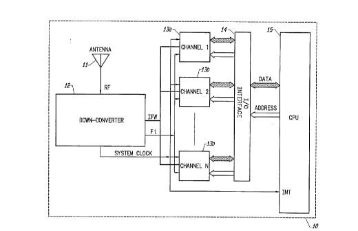
Referring to Figure 14, a general block
diagram of a pseudo-random noise (PRN) receiver 10 that
implements the present invention. The receiver lO
,
CA 02229069 1998-02-09
W O 97/~6446 PCT~US96/12967
includes an antenna 11, a downconverter 12, multiple
channels 13a to 13n, an input/output interface 14, and
a digital processor 15. The antenna 11 receives a
composite signal RF, composed of signals from all
satellites in the system that are directly in the line
of sight of the antenna. The composite signal RF is fed
to the down-converter 12 to provide a quantized and
sampled intermediate frequency signal IFW, a system
sampling clock Ft and a SYSTEM CLOCK.
The signal IFW is a word of 4 bits, each
representing one of four IF consecutive samples at a Fs
sa~pling rate. The processing clock Ft is a division by
~4 of the Fs signal. The system clock is a further
division of Ft signal, interrupting the processor at a
rate of approximately 1 per millisecond and triggering
the channel processing.
Referring to Figure 15, the down-converter is
discussed. The RF signal is first prefiltered by the RF
filter 120, amplified by 121, and mixed with the Local
Oscillator (LO) by the mixer 122, filtered and amplified
again in IF by 123 and 124, and finally quantized in one
bit by the hard limiter 125. The filter 123 is in fact
used as a pre-correlation filter with a two-sided
bandwidth of 20.46Mhz. The instantaneous hard limiter
output is sampled at a rate of Fs, and shifted in the 4-
stage shift register 126. The sampling rate Fs is
chosen to satisfy the Nyquist rate requirement, related
to the pre-correlation filter bandwidth. Every Ft clock
transition (i.e. 4 Fs clocks), the full contents of the
shift register is transferred into a parallel register
127. The 4 bit word IFW is then transferred to the
channel circuits at a Ft rate for satellite individual
tracking.
The clock reference circuitry of the down
converter (Figure 15) includes a phase lock loop (PLL)
which is composed itself of the voltage controlled
,
CA 02229069 1998-02-09
W O 97/06446 PCT~JS96/12967
23
oscillator (VCO) 131, a frequency divider 132, a phase
comparator 129, which compares the phase with a stable
reference oscillator 128, and, finally, a low fre~uency
loop filter 130. The VCO output is used as local
oscillator for the RF section. The frequency of the VCo
131 is divided in several steps, a first time by a
divider 133 to get the sampling frequency Fs, a second
time by a divider 134 to get the processing clock Ft,
and a third time by a divider 135 to get the SYSTEM
CLOCK.
As shown in Figure 14, the sampled and
quantized intermediate frequency signal IFW is
simultaneously fed to each of the several signal
processing channels 13a to 13n. A separate channel 13
is devoted to every visible satellite; the assignment to
a given satellite is made by configuring the pseudo-
random noise (PRN) generator through the PRN GENERATOR
COMMANDS. The structure of a channel 13, typical of
each of the channels 13a-13n, is given in Figure 16.
Every satellite signal is simultaneously tracked in
carrier phase by a carrier Phase Lock Loop(PLL) and in
code phase by a Delay Lock Loop (DLL). All channel
processing is made in a fully synchronous manner at a
processing clock Ft. IFW samples are processed 4 by 4,
and all carrier and code generation is made at Ft rate
by groups of 4 as well.
Both the PLL and the DLL are implemented
partly in the channel 13, and partly in the processor
15. The link is made by the I/O interface 14. The loop
comparators and the loop actuators are located in each
channel, whereas the filter implementation and the loop
management are handled by the processor 15. The loops
are updated when the processor is interrupted by the
SYSTEM CLOCK signal and the MEAS READY signal is set for
that channel, informing the processor that a measurement
cycle has just finished. All measurement cycles are
CA 02229069 1998-02-09
W O 97/06446 PCTrUS96/12967
24
chosen at a period bigger than that of the SYSTEM CLOCK,
in order not to miss any measurement. The cycle period
is set by the processor at every channel initialization,
through the PRN GENERATOR COMMAND.
The carrier PLL uses the measurements I and Q
of an in-phase correlator 130a, and a quadrature phase
correlator 130b. In a tracking mode, the PLL drives the
information Q to zero while checking for the presence of
the signal locking on I. Both correlators are using the
same "punctual" pseudo-random code (PRN) for the
correlation, but use different~carrier signals COS and
SIN. The processed information is used to control the
CARRIER FREQUENCY COMMAND of a carrier numerically
controlled oscillator (NCO) 132.
The carrier NCO 132 is described in detail in
Figure 17. The instantaneous carrier phase image is
kept in a carrier phase register 1325, where the total
range represents 2~ of carrier phase. The current
CARRIER FREQU~NCY COMMAND is kept in a frequency command
register 1323. At every ~t transition, this value is
added to the current carrier phase register contents by
the adder 1321c; thus, the carrier phase is incremented
one full cycle every time the carrier phase register
1325 cycles back to zero.
The instantaneous carrier phase can be
obtained at any SYSTEM CLOCK transition or at every Ft
very straightforwardly; the carrier phase register 1325
is reset synchronously with the SYSTEM CLOCK at the
initial CHANNEL RESET command, ensuring a known initial
phase. Every processor command loaded into a buffer
1324 is transferred into the frequency command register
1323 and effective at the next SYSTEM CLOCK transition;
as the SYSTEM CLOCK period is an exact number of Ft
periods and knowing the loaded command word, the exact
value in the carrier phase register is obtained at the
CA 02229069 l99X-02-09
PCT~US96/12967
W O 97/06446
next SYSTEM CLOCK transition or at any Ft clock
transition in between by direct computation.
The one bit reference carrier cosine value C0
is obtained by "exclusively ORing" the most significant
bit (MSB) and the second most significant bit of the
carrier phase register contents. The one bit reference
carrier sine value is obtained using the MSB of carrier
phase register contents; this is actually done in the
phase/quadrature signal generator 1320c.
As the samples are processed 4 by 4, the
carrier references are generated synchronously with the
exact sampling times for the 3 other samples as well.
~Arbitrarily and for simplicity o~ implementation, the
reference signal is chosen to be the third of the
sequence of 4.
If may be noted that the carrier phase 1325 is
physically incremented by the frequency command value
1323 every Ft. It is equivalent to say that the
instantaneous carrier phase is virtually incremented by
a fourth of this value every Fs (i.e. four times per Ft
period). As a result, the reference carrier phase
synchronous with the ~ourth sample (most recent one) is
obtained by adding frequency command divided by four
(divider 1322c) to the current carrier phase 1325; the
Z5 carrier cosine (sine) value C+l (S~l~, delayed of one
sampling period, is obtained from it with the phase
quadrature signal Generator 1320d using the same
algorithm as for C0 and s0.
Similarly, C2, S2 are obtained by subtracting
frequency command value divided by 2 using 1322a from
the current carrier phase 1325. This substraction is
per~ormed by using the adder 1321a. The cosine and sine
values are finally obtained through 132~a.
Finally C~,S_l are obtained ~y subtracting the
frequency command value divided by 4 using 1322b from
the current carrier phase 1325. This substraction is
CA 02229069 1998-02-09
W O 97/06446 PCTAJS96/12967
made using the adder 1321b. The cosine and sine values
are ~inally obtained ~hrough 132Qb.
The full NCO output is a "cosine" word COS and
a "sine" word SIN of 4 bits each, each bit being the
sampled carrier reference value one sample apart. The
"punctual" in-phase (130a) and quadrature-phase ~130~)
correlators for the PLL are described in Figure 19.
Given the close similarity, the following correlator
description deals with only the in-phase case.
The intermediate frequency word IFW composed
of 4 samples is "exclusive ORed" with the 4 bit cosine
carrier reference COS in the structure 1301a to 1301d.
All samples are added in the adder 1302; the result is
comprised between -4 and ~4 (the "0" values are
processed as "-1" by the adder 13023. The result is
then multiplied by the value of reference PRN sequence
synchronous with the most recent sample (multiplier
1303). The resulting value is then algebraically added
at a Ft rate to the current contents of the accumulator
1305. At every CYCLE transition the accumulator value
is transferred to the buffer, the accumulator is reset,
and finally a new measurement period is initiated. The
processor is then able to read the measurement values to
close the loops.
Going briefly back to Figure 16, the delay
lock loop will be described in more detail. The DLL has
2 configurations, acquisition mode or tracking mode,
depending on the channel locking phase. As described in
the prior section, the tracking mode pre~erably uses an
"edge DLL" correlator, while the acquisition mode uses
a O.l chip delay DLL. The selection between 2 modes is
made through the signal DLL SELLCT. Other specific
combinations of tracking and acquisition mode
correlators may also be employed.
~- The delay lock loop (DLL) processing is timed
at a Ft rate similarly to the PLL, and the measurement
CA 02229069 1998-02-09
W O 97/06446 PCT~US96/12967
update rate is CY~LE as well. The DLL uses dI and dQ
information coming from an in-phase DLL correlator 131a
for dI, and a quadrature phase DLL correlator 131b for
dQ. The DLL drives the dQ value to zero when in
tracking mode. The dQ is used in conjunction with dI
when in acquisition mode. The processed information is
used to control the PRN GENERATOR COMMANDS of the PRN
Code Generator 133.
The "edge DLL" principle, previously described
with respect to Figures 10, llD and 12, will be
described in more detail, in light of the GPS receiver
just described. For "edge DLL" implementation purposes,
four time intervals of equal duration have to be defined
around the PRN code transition; two before the code
transition and two after. In the current embodiment,
each time interval has an exact duration of 1/Fs or the
IF sampling period.
We thus infer that every time interval
contains one and only one IF sample at a Fs rate. The
relative position of the samples in the interval is
unknown and depends on the relative phase between code
generator and sampling clock. The full formula
expressing the DLL response is given below.
Assume that S_2, S " S+l, S+2 is a sequence of
four consecutive IF samples with the code transition
between Sl and S+l, and the associated sampled PRN code
CA 02229069 1998-02-09
PCT~US96/12967
WO 97/06446
28
sequence is PRN2, PRN_l, PRN~l, PRN,2 (with PRN_2 = PRN_
and PRN~l = PRN+2). dPRN may be defined as:
dPRN = 1 . (PRN~1 -PRN, )
Thus dPRN equals:
+1, if the transition is a rising edge,
-1, if the transition is a falling edge,
~ 0, if two consecutive PRN chips a~e identical.
dPRN can be thought as the derivative of the PRN
sequence.
At every PRN chip code transition, the
lo elementary DLL contribution is given by:
DLL j = (-S -2tS_~ tS1l -St2)~dP~N
The contribution is not zero if dPRN¢0 (i.e. if PRN_
¢ PRN~
After an integration period defined between
two contiguous CYCLE transitions, the full DLL
response will be:
DLL= ~: DLLi
This summation performs a low pass frequency filtering
function of the measurements dI and dQ.
Going back to the physical implementation, we
notice that knowing a code transition falls inside a
CA 02229069 1998-02-09
W O 97/06446 PCT~US96/12967
29
group of 4 IFW samples, we still have to know between
which samples of the group the code transition falls.
The signals P0 and P1 show where the code transition
falls among the 4 IFW samples. Because we need to add
5 4 consecutive values and the code transition can have 4
different positions in the sequence, we need to keep the
3 previous samples of the previous sequence of 4 IFW.
The total sequence will be, from the oldest sample to
the newest: S2A~ S3A~ S~A~ S1~ S2, S3, S4 and PRN4 being
lO the PRN code synchronous with S,
P1 PO code Elementary DLL Elementary DL~ operation
valu ? value transition operation in tracking in acquisition mode
falls mode
~etwe~
~ ~A anc 4A (- ~A+S3A+ S4A -S1~2dPRN (+ ~A +S~A+S4A+S1)~dPRN
L5 1 4A ~nc 1 (~ ~A +S4A+S1 S~3~dPRN (+ ~A +S4A+S1+ ~dPRN
O ' 1 anc ~, (~ 4A+S1 +S~-S3~dPRN (+ 4A+S~ +S~+S ~, ~dPRN
1 ~ and S~ ( _1+S~+S~-S4)OEIdPRN (S~+S~+S,,+S4)~CPRN
Table 1
Going to Figure 20, the implementation of the
In-Phase DLL correlator 131a is described in detail.
After multiplying IFW by the Carrier word COS by 1310a
25 to 1310d, the three last samples of the current IFw word
are latched in 1318. At the input of the ~our
multiplexors 1311a to 1311d, seven samples are
simultaneous available, S1 to S4 from the current IFW and
SZA to S4A from the preceding one. Depending on the
30 current value of Pl and P0, a common selection is made
on all 4 multiplexors. For the remaining of the
explanation, we will assume that P0=Pl=0. On 1311a
output, S1 is available; on 1311b, S4A is available, and
so on. The adder 1313 adds up all selected samples
35 ~interpreting "0" inputs as "-1" value in the process).
The result is then multiplied }~y dPRN to form the
elementary value DLL$. In tracking mode, the signal DLL
CA 02229069 1998-02-09
WO 97/06446 PCT~USg6/12967
SELECT will invert the values coming out from the first
and the last multiplexor, thus ful~y implementing the
tracking DLL formula described in the first line of the
Table 1.
The current value between +4 and -4 is
algebraically added to the accumulator 1316 by the adder
1315 during the same Ft transition. Every transition on
CYCLE transfers the accumulator value to the bu~fer
1317, resets the accumulator, and finally initiates a
lo new measurement period.
There is only a slight difference when
implementing the acquisition mode. The circuitry is
~identical up to the adder 1313, except that the first
and last sample coming out from the multiplexor 1311a
and 1311d are not inverted. The dPRN signal is defined
the same way than previously, but its size is expanded
to reach 0.1 code chip duration, centered on the code
transltion.
Re~erring to Figure 18, the full PRN code
generator will be described. The Generator is in fact
composed of a code numerically controlled oscillator
(NCO), which delivers a chip frequency clock FC whose
frequency is in direct control of the processor through
the CODE FREQUENCY COMMAND; in turn, Fc clocks the PRN
code generator 1334 per se.
Let's begin by the Code NCO description:
similarly to the carrier NCO, it is embodied by a code
phase register 1335, whose full range represents 2~ of
the code phase. At every Ft transition, the word into
code ~requency command register 1336 is added (modulo
the range of code phase register) to the contents of the
code phase register by the adder 1331d. The carry
signal coming ~rom the adder is used as chip frequency
Fc. The CODE FREQUENCY COMMAND word present in the code
frequency command register is loaded at every SYSTEM
CLOCK transition from the buffer 1337. The buffer is
CA 02229069 1998-02-09
W O 97/06446 PCT~US96/12967
itself loaded from the processor at any time. Another
important function of the code NC0 is to deliver the
signals P0 and P1, whose function was described earlier.
The P~ and P1 signals are generated as
follows: if R is the total range of the code phase
register (CPR) 1335, and ~ is the phase increment at
every Fs sample (~ = CODE FREQUENCY COMMAND /4).
0<CPR~ ~cCPR~ 2~<~PR~ R-2~<CPR<R- R-~<CPR~R
~ 2~ R-2~ ~
Pl 0 ~ 1 1 1
~0 1 0 ~ 1 0
Table 2
Pl is obtained by subtracting the Code
Frequency Register (CFR) 1336 divided by two (by divider
15 1332b) from the Code Phase Register (CPR) 1335 by use
of the adder 1331c. If the result RESl is positive, P1
= 1.
The P0 case is different depending on the Pl
value. If P1 is zero (CPR <2~), CFR, divided by four
20 (by divider 1332a), is multiplied by -1 in the
multiplier 1331b; if P1 is one (CPR~2~), CFR/4 is
multiplied by +1. Then 1331a adds RES1 to the
multiplication result; the carry of the adder 1331a is
taken as P0. The final result is in agreement with
Table 2.
The PRN code generator 1334 is clocked by the
chip frequency Fc. It is configured for a particular
satellite sequence by the command GENERATOR PRESET. It
outputs an epoch signal, synchronous with a particu-ar
instant in the PRN sequence, which is taken as reference
in the PRN ranging sequence. The data bits superimposed
on the PRN sequence have their transition perfectly
synehronous with this epoch signal.
CA 02229069 1998-02-09
W O 97/06446 PCT~US96/12967
The EPOCH signal clocks the cycle counter
1333, which is reset at the initialization of the
channel by the SYNC RESET, and counts an integer number
of epochs (preset at the preset sequence) be~ore to
generate a transition on CYCLE, which stops the current
measurement cycle on all correlators and informs the
processor by the signal MEAS READY. Every channel has
its own cycle counter, synchronized on its own data
transitions. After a synchronizing phase on the data
lo transitions, it is possible to slow down the measurement
periods up to 2Oms, no data transitions occurring during
this period.
It is assumed, accurately, that the edge DLL
correlator used on C/A code, with a precorrelation
bandwidth prefiltering (typically 20.46Mhz double
sided) improves the multipath error. A PRN code
transition detector is built X-ORing the current code
output and the previous one latched in the latch 1339.
The signal dPRN is generated by 1338 according to the
description in the DLL principle explanation.
According to the usual multipath model, the
direct received signal is given by:
A PRN( t) cos(~Ot+~)
where:
A is the amplitude of the received signal~5 PRN(t) is the pseudo-random sequence
is the carrier frequency pulsation
is the carrier phase offset
CA 02229069 1998-02-09
W O 97/06446 PCTAUS96/12967
The multipath signal is given by:
A ~ a PRN (t ~ cos (~o( t - ~) + (p
where:
~ is the amplitude ratio between direct and
multipath signal
1 is the propagation delay between direct and
multipath signal
a is the additional phase rotation between direct and
multipath signal.
The main effect of the presence of a multipath
signal is to shift the zero crossing of the DL~ response
from the "zero multipath" reference differently for each
of the three discriminators. The DLL driving the DLL
correlator output to zero in average, the difference
between zero crossings will be seen directly as an error
in the measured code phase. As the different satellites
on which the channels do not experience the same
multipaths because of a different geometry, the position
computation will be erroneous.
Returning to the above description, with
respect to Figures llD and 12, of operation of a
receiver that uses the demodulation technique of Figure
10, a few alternate local gating sequences will be
described. Figures 21B, 21C and 21D give other examples
of what the gating signal generator 343 can provide in
2~ line 341. ~he result in terms of the error signal
characteristic of Figure 9D is substantially the same,
but the different gating sequences of Figures 21B-D
cause the height and duration of the non-zero portions
of the Figure 9D curve to change somewhat. The
fundamental advantage is retained, however, of providing
extended intervals where the error signal is zero.
CA 02229069 l998-02-09
W O 97/06446 PCT~US96/12967
34
In each of ~igures 21B-D, a carefully
controlled gating signal occurs at each of transitions
365, 367, etc., of the incoming code (Figure 21A). In
Figure 21B, negative portions 369 and 37~ of the signal
have a magnitude less than 1, while corresponding
positive portions 373 and 375 have a magnitude of 1.
The lower magnitude negative portions of the signal are
given longer durations, however, so that the areas of
the pulse portions 369 and 373 are equal, as are the
areas 371 and 375. In the gating signal of Figure 21C,
a positive area 377 ~magnitude less than 1) is much
smaller than a negative area 379 tmagnitude more than
~l), while a positive area 381 is much smaller than a
negative going area 383. This gating signal differs
from the others shown herein by aligning with the code
signal edge 365 (when a minimum error condition exists)
a transition between negative and positive going
portions of the signal. Each of the signals of Figures
llD, 12, 21B and 21C is symmetrical about-the code edge.
The signals are positioned with their middle aligned
with the code edge.
In Figure 21D, however, the gating signal is
non-symmetrical about the incoming code edge. But the
positive and negative going pulse portions have equal
areas on each side of the code edge. That is, areas 385
and 387, on one side of the code edge 365, are
substantially equal, while the areas 389 and 391 on the
other side of the code edge 365 are also substantially
equal.
Although several specific examples of compound
gating pulse shapes have been given, there are numerous
other shapes, with various relative magnitudes, that can
be employed instead. The total negative and positive
going areas of any such compound gating pulse is made to
be~ substantially equal. This property causes the
multipath signal to be substantially eliminated so long
CA 02229069 1998-02-09
W O 97/06446 PCTAJS96/12967
as its delay from the line of sight signal is
sufficient.
Although the various aspects of the present
invention have been described with respect to their
preferred implementations, it is understood that the
invention is protected within the full scope of the
appended claims.