Note: Descriptions are shown in the official language in which they were submitted.
s
CA 02229179 2000-10-13
DESCRIPTION
IC CARD READER/WRITER AND ITS CONTROL METHOD
TECHNICAL FIELD
The invention relates to an IC card reader/writer
which reads data from and writes data to IC (integrated
circuit) cards~I~aving integrated circuits mounted
thereon; in particular, it relates to an IC card
reader/writer having improved reliability which can
reliably detect a contact error with respect to a contact
section which is brought into contact with an integrated
circuit mounted on an IC card at the time of reading data
from and writing data to the IC card, and a method of
controlling the same.
BACKGROUND ART
Recently, IC cards having integrated circuits mounted
thereon have been devised for use as various types of
cards such as bank cards etc. As these IC cards are able
to store significantly more information than previous
magnetic cards etc., they have the advantage of greatly
increasing the types of usage possible.
However, with IC card reader/writers which read data
from and write data to'IC cards, when data is read from
or written to the integrated circuit mounted on the IC
card, this is carried out through the contact section
which is brought into contact with integrated circuit
1
CA 02229179 1998-02-10
terminals, and a problem therefore exists in terms of the
possibility of poor contact, that is to say contact
error, at the contact section.
In prior IC card reader/writers, in order to judge
whether or not the contact section was in proper contact
with the integrated circuit terminals, under conditions
in which the contact section of the IC card reader/writer
was in contact with the integrated circuit terminals of
the IC card, IC card power was supplied to the IC card's
integrated circuit power supply terminal from the IC card
reader/w:riter, through the contact section; together with
this, a ~~lock signal was supplied to the IC card's
integrat~sd circuit clock terminal through the contact
section; in addition, the IC card's integrated circuit
reset terminal was set to a high level; thereafter, the
data which was automatically outputted from the IC card's
integrated circuit input/output terminal was read; and
judgement was made as to whether the IC card
reader/w:riter contact section was in proper contact with
the IC c~3rd's integrated circuit terminals, according to
whether or not the read-out data was the same as the
expected data.
However, in the conventional IC card reader/writers
described above, wherein a clock signal is supplied to
the IC card's integrated circuit clock terminal, the IC
card's integrated circuit reset terminal is set to a high
level, and thereafter, judgement is made as to whether or
not the contact section of the IC reader/writer is
2
CA 02229179 1998-02-10
properly in contact with the IC card's integrated circuit
terminals, according to whether or not the data
automatically outputted from the IC card's integrated
circuit input/output terminal is the same as the expected
data, there has been a problem in so much as there are
cases wherein, for example, even if contact with the IC
card's integrated circuit power supply terminal is poor,
signals supplied to other terminals of the IC card's
integrated circuit flow within the IC card's integrated
circuit .and are used as power; in such cases, regardless
of the fact that the contact section of the IC card
reader/w:riter is not in proper contact with the IC card's
integrat~ad circuit terminals, data which is the same as
the expe~~ted data is output from the input/output
terminal of the IC card's integrated circuit; and based
on this, the contact section of the IC card reader/writer
is mistakenly determined to be in proper contact with the
IC card';s integrated circuit terminals.
In such cases, while power sufficient for reading
data from the IC card's integrated circuit input/output
terminal may have been supplied, this power is not
sufficient for writing data through the IC card's
integrated circuit input/output terminal and, where data
write processing is carried out through the IC card's
integrated circuit input/output terminal in this
condition, write errors sometimes occur.
There has been a problem in that, in general, when
write er:cors of this sort occur with respect to IC cards,
3
CA 02229179 1998-02-10
the security data which is stored in the integrated
circuit may be destroyed, and in this case, further use
of the card becomes impossible.
An object of the present invention is to provide an
IC card reader/writer and a method for controlling the
same, wherein contact errors with respect to a contact
section which is brought into contact with an integrated
circuit mounted on an IC card are reliably detected, and
whereby it is possible to carry out suitable processing
before write errors with respect to the IC card occur.
DISCLOSURE OF THE INVENTION
In order to achieve the object described above, the
present invention provides an IC card reader/writer
having a contact section which is brought into contact
with terminals of an integrated circuit mounted on an IC
card, for reading data from and writing data to the
integrated circuit through the contact section,
characterized in that the IC card reader/writer
comprises:
contact error detection means for controlling a reset
signal supplied to a reset terminal of the integrated
circuit through the contact section to a low level, for
controlling a clock signal for the integrated circuit
supplied to a clock terminal of the integrated circuit
through 'the contact section to a low level, thereafter,
for supplying power for the integrated circuit to a power
supply terminal of the integrated circuit through the
4
CA 02229179 1998-02-10
contact aection and for detecting a contact error with
respect to the contact section, when a voltage outputted
from an input/output terminal of the integrated circuit
through 'the contact section is lower than a predetermined
reference voltage.
The contact error detection means may be configured
such that, after the power for the integrated circuit has
been supplied to the power supply terminal of the
integrated circuit, it supplies the clock signal to the
clock terminal of the integrated circuit for a
predetermined period of time within which resetting of
the integrate circuit is normally terminated and,
thereafter, controls the clock signal again to the low
level.
Furthermore, the IC card reader/writer comprises:
integrated circuit clock generation means for
generating the clock signal for the integrated circuit;
and
integrated circuit power supply means for generating
the power for the integrated circuit;
wherein the contact error detection means comprises:
first control means for controlling the reset signal
supplied to the reset terminal of the integrated circuit
through -the contact section to the low level;
second control means for controlling the clock signal
for the :integrated circuit supplied to the clock terminal
of the integrated circuit through the contact section to
the low :Level, by controlling the integrated circuit
CA 02229179 1998-02-10
clock signal generation means;
third control means for supplying the power for the
integrated circuit to the power supply terminal of the
integrated circuit through the contact section, by
controlling the integrated circuit supply generation
means; and
comparison means for comparing the voltage outputted
from the input/output terminal of the integrated circuit
through the contact section with the predetermined
reference voltage.
Furi:hermore, the IC card reader/writer may further
comprise a central processor unit, wherein the first
control :means, the second control means and the third
control means are realized by the central processor unit.
The configuration may be such that the comparison
means is realized by the central processor unit.
Furthermore, the configuration may be such that, the
clock signal generation means for the integrated circuit
is also 'used as clock signal generation means for the
central ;processor unit, which supplies the clock signal
to the central processor unit.
Furthermore, the configuration may be such that, the
power supply means for the integrated circuit is used as
power supply means for the central processor unit, which
supplies power to the central processor unit.
Furthermore, the present invention provides a method
of controlling an IC card reader/writer having a contact
section which is brought into contact with terminals of
6
CA 02229179 1998-02-10
an integrated ClrCUlt mounted On an IC card, for reading
data from and writing data to the integrated circuit
through 'the contact section, characterized in that the
method comprises:
a first step of controlling a reset signal supplied
to a reset terminal of the integrated circuit through the
contact section to a low level;
a second step of controlling a clock signal for the
integrated circuit supplied to a clock terminal of the
integrated circuit through the contact section to a low
level, under a condition wherein the reset signal
supplied to the reset terminal of the integrated circuit
through 'the contact section is controlled to be the low
level in the first step;
a third step of supplying power for the integrated
circuit to a power supply terminal of the integrated
circuit 'through the contact section, after controlling
the clock signal for the integrated circuit supplied to
the clock terminal of the integrated circuit through the
contact section to the low level in the second step; and
a fourth step of detecting a contact error with
respect to the contact section, if a voltage outputted
from an .input/output terminal of the integrated circuit
through 'the contact section is lower than a predetermined
reference voltage when the power for the integrated
circuit .is supplied to the power supply terminal of the
integrated circuit through the contact section in the
third step.
7
CA 02229179 1998-02-10
The invention may be configured to further comprise:
a fifth step of supplying the clock signal to the
clock terminal of the integrated circuit for a
predetermined period of time within which resetting of
the integrated circuit terminates normally, after
supplying the power for the integrated circuit to the
power supply terminal of the integrated circuit in the
third step; and
a sixth step of controlling the clock signal once
again to the low level, after supplying the clock signal
to the clock terminal of the integrated circuit in the
fifth step.
With such configurations, a contact error with
respect to a contact section which is brought into
contact with an integrated circuit mounted on an IC card
can be reliably detected, and it is possible to perform
suitable processing before the occurrence of write errors
with respect to the IC card.
BRIEF DESCRIPTION OF THE DRAWINGS
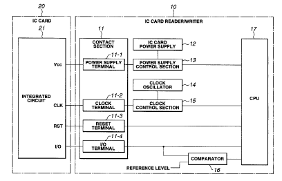
Fig. 1 is a block diagram showing the overall
structura_ of an IC card reader/writer control system
according to the present invention; and
Fig. 2 is a flow chart showing the processing details
for the :IC card reader/writer shown in Fig. 1.
BEST MODE FOR CARRYING OUT THE INVENTION
The following is a detailed explanation of one
8
CA 02229179 1998-02-10
embodiment of the IC card reader/writer according to the
present invention in accordance with the attached
figures.
Fig. 1 is a block diagram showing the overall
structure of the control system for IC card reader/writer
according to the present invention; as this IC card
reader/w:riter 10 reads data from and writes data to
integrated circuit 21, which is mounted on IC card 20, it
is constructed so as to comprise: contact section 11
which is brought into contact with terminals of
integrated circuit 21 of IC card 20; IC card power supply
12 which generates IC card power, which is supplied to
power supply terminal Vcc of integrated circuit 21
through contact section 11; power supply control section
13 which controls the IC card power generated by IC card
power supply 12; clock oscillator 14 which generates IC
card clock which is supplied to clock terminal CLK of
integrated circuit 21 through contact section 11; clock
control section 15 which controls the clock generated by
clock oscillator 14; comparator 16 which compares a
signal generated by input/output terminal (I/O terminal)
of integrated circuit 21 of IC card 20 and which is
inputted through contact section 11 with a predetermined
reference level; and central processor unit (CPU) 17
which controls power supply control section 13 and clock
control :section 15, and also: carries out processing
which supplies a reset signal to the reset terminal RST
of integrated circuit 21 through contact section 11;
9
CA 02229179 1998-02-10
carries out processing which reads data from and writes
data to the input/output terminal of integrated circuit
21 of IC card 20 through contact section 11; and carries
out processing which detects a contact error with respect
to contact section 11 based on the output of comparator
16, etc.
Furthermore, contact section 11 comprises: power
supply terminal 11-1, clock terminal 11-2, reset terminal
11-3 and input/output terminal 11-4, which are brought
into contact with, respectively, power supply terminal
Vcc, clock terminal CLK, reset terminal RST and
input/output terminal I/0 of integrated circuit 21 of IC
card 20.
Further, the IC card power supply 12 may be used as
the IC card reader/writer 10 power supply.
Furthermore, the clock oscillator 14 may be used as
the clock generator which supplies the CPU clock signal
to the central processor unit (CPU) 17 of IC card
reader/writer 10.
Furthermore, the comparator 16 may be configured with
the use of the input section of such logical ICs as TTL,
CMOS etc., which are installed within the central
processor unit (CPU) 17 of IC card reader/writer 10.
The following is an outline of detection processing
for errors in contact section 11 of IC card reader/writer
according to the aforementioned configuration.
1) ay inserting IC card 20 into the IC card insertion
slot (not shown in the diagram of IC card reader/writer
CA 02229179 1998-02-10
10), power supply terminal Vcc, clock terminal CLK, reset
terminal RST, and input/output terminal I/0 of integrated
circuit 21 of IC card 20 are brought into contact with
power supply terminal 11-1, clock terminal 11-2, reset
terminal 11-3 and input/output terminal 11-4 of contact
section 11 of IC card reader/writer 10.
2) The reset signal, which is supplied to reset
terminal RST of integrated circuit 21 of IC card 20, is
caused to be low-level by means of central processor unit
(CPU) 17 of IC card reader/writer 10.
3) Clock control section 15 is controlled by means of
central processor unit (CPU) 17 of IC card reader/writer
and, thereby, the clock signal which is supplied to
clock terminal CLK of integrated circuit 21 of IC card 20
is caused to be low-level.
4) Power supply control section 13 is controlled by
means of central processor unit (CPU) 17 of IC card
reader/writer 10 and, thereby, IC card power which is
generated by IC card power supply 12 is supplied to power
supply terminal Vcc of integrated circuit 21 of IC card
20.
5) A clock signal is supplied to clock terminal CLK
of the integrated circuit 21 for a period of time within
which resetting of integrated circuit 21 of IC card 20
terminates normally and, thereafter, the clock signal is
controlled so as to be low-level once again.
6) The voltage generated at the input/output terminal
(I/O terminal) of integrated circuit 21 of IC card 20 is
11
CA 02229179 1998-02-10
compared with a predetermined reference level by
comparator 16 of IC card reader/writer 10.
7) In cases where the comparison result of comparator
16 indicates that the voltage generated by the
input/output terminal (I/O terminal) of integrated
circuit 21 of IC card 20 is lower than a predetermined
reference level, central processor unit (CPU) 17 of IC
card reader/writer 10 judges that a contact error has
occurred for contact section 11.
The reason for providing the processing expressed in
5), that is, in other words, processing wherein, after
power has been supplied to power supply terminal Vcc of
20 integrated circuit 21 of IC card 20, a clock signal is
supplied to clock terminal CLK for a period of time
within which resetting of integrated circuit 21 of IC
card 20 terminates normally and, thereafter, the clock
signal is controlled so as to be low-level once again, is
to make .reliable detection of contact errors with respect
to the contact section possible, even in cases where
integrated circuit 21 mounted on IC card 20 is such a
type of integrated circuit that causing the rest signal
which is supplied to reset terminal RST to be low level,
causing 'the clock signal which is supplied to clock
terminal CLK to be low level and, thereafter, supplying
power to power supply terminal Vcc alone does not result
in a stable condition.
In other words, depending on the type of integrated
circuit 21 mounted on IC card 20, causing the rest signal
12
CA 02229179 1998-02-10
which is supplied to reset terminal RST to be low level,
causing the clock signal which is supplied to clock
terminal CLK to be low level and, thereafter, supplying
power to power supply terminal Vcc alone may not result
in a stable condition for the integrated circuit 21
mounted on IC card 20.
So as to allow for this, the present embodiment is so
structured that, after supplying power to power supply
terminal Vcc of integrated circuit 21 of IC card 20, a
clock signal is supplied to the clock terminal CLK for a
predetermined period of time, thereby waiting for the
normal termination of the resetting of the integrated
circuit 21, and thereafter, the clock signal which is
supplied to clock terminal CLK of the integrated circuit
21 is once again controlled so as to be low-level.
Further, in cases where the integrated circuit 21
mounted on IC card 20 is of such a type that causing the
rest signal which is supplied to reset terminal RST to be
low level, causing the clock signal which is supplied to
clock terminal CLK to be low level, and thereafter,
supplying power to power supply terminal Vcc alone
results in a stable condition, the processing expressed
in the aforementioned 5) is nat necessary.
Furthermore, in cases where the comparison result of
comparator 16 indicates that the voltage generated at the
input/output terminal (I/O terminal) of integrated
circuit 21 of IC card 20 is greater than a specified
reference level, contact section 11 of IC card
13
CA 02229179 1998-02-10
reader/writer 10 may be considered to be in proper
contact with the various terminals of integrated circuit
21 of IC card 20 and, therefore, central processor unit
(CPU) 17 of IC card reader/writer 10 controls clock
control section 15 so that: the IC card clock generated
by clock oscillator 14 is supplied to clock terminal CLK
of integrated circuit 21 of IC card 20; the reset signal
which is supplied to reset terminal RST is caused to be
high-level; the data which is automatically output from
the input/output terminal (I/0 terminal) of integrated
circuit 21 of IC card 20 is, as a result of this, read;
and checking is carried out in the same way as
previously, so as to verify whether or not this data is
the same as the expected data.
Fig. 2 shows details of the aforementioned processing
which detects contact errors with respect to contact
section 11 in IC card reader/writer 10, in the form of a
f low chart .
Accarding to Fig. 2, the power supply (not shown in
the diagram of IC card reader/writer 10) is first turned
ON (step 101). Following this, power supply control
section .13 is controlled so that the IC power is OFF, the
reset signal which is supplied to reset terminal RST of
integrated circuit 21 of IC card 20 is caused to be low-
level and the clock signal which is supplied to clock
terminal CLK of the same is caused to be low level (step
102).
Next, the system waits for the insertion of IC card
14
CA 02229179 1998-02-10
20 (step 103); when IC card 20 is inserted, by virtue of
pressing together the terminal section of IC card 20 and
contact section 11, contact is made between the various
terminals of IC card 20 and contact section 11 (step
104). Further, in cases where IC card reader/writer 10 is
constructed so that the terminal section of IC card 20
and contact section 11 are automatically pressed together
when IC card 20 is inserted, the processing in this step
(104) is not necessary.
Next, power supply control section 13 is controlled
so that IC power is turned ON (step 105); a clock signal
is supplied to clock terminal CLK (step 106); and normal
termination of resetting is verified (step 107).
Thereupon, in cases where resetting has terminated
normally (YES for step 107), the clock signal which is
supplied to clock terminal CLK is once again caused to be
low-level (step 108).
Next, the voltage at input/output terminal (I/0
terminal) of integrated circuit 21 of IC card 20 is
judged by means of comparator 16 (step 109). In other
words, the voltage at the input/output terminal (I/O
terminal) of integrated circuit 21 of IC card 20 is
compared with a predetermined reference level.
In the case of abnormalities, in other words, in
cases where the voltage at the input/output terminal (I/O
terminal) of integrated circuit 21 of IC card 20 is less
than a predetermined reference level, contact section 11
of IC card reader/writer 10 is not properly in contact
CA 02229179 2000-10-13
with the various terminal of integrated circuit 21 of IC
card 20 and, therefore, the user is informed of the fact
that IC card 20 must be reinserted (step 110).
In this case, reset terminal RST of integrated
circuit 21 of IC card 20 is set to a low level, clock
terminal CLK is set to a low level and IC card power is
turned OFF (step 120); IC card 20 is ejected (step 121)
and step 103 .is returned to.
Further, the configuration may be such that, in step
110, instead of informing the user of the fact that IC
card 20 must be reinserted, IC card 20 is automatically
reinserted and another attempt is made.
Furthermore, if the result of step 109 is normal, in
other words, in cases where the voltage at the
input/output terminal (I/O terminal) of integrated
circuit 21 of IC card 20 is greater than a predetermined
reference level: clock control section 15 is controlled
so that a clock signal is supplied to clock terminal CLK
of integrated circuit 21 of IC card 20 (step 111); the
reset signal supplied to reset terminal RST is caused to
be high level (step 112); and the ATR information from
the input/output terminal (I/O terminal) of integrated
circuit 21 of IC card 20 is acquired.(step 113).
Thereupon_reception conditions are judged from this
Answer to Rest (ATR) information (step 114).
In cases where an error has occurred: step 110 is
proceeded to;.the user is informed of the fact that IC
card 20 must be reinserted ; reset terminal RST.of
16
CA 02229179 1998-02-10
integrated circuit 21 of IC card 20 is set to a low
level; clock terminal CLK is set to a low level; IC card
power is turned OFF (step 120); IC card 20 is ejected
(step 121); and step 103 is returned to.
Further, in step 121, instead of ejecting IC card 20,
the configuration may be such that withdrawal of the IC
card is made possible, or such that the user is informed
of the fact that IC card 20 can be removed.
In cases where no errors occur in step 114, judgement
is next made as to whether the inserted IC card 20 is a
usable card or not (step 115).
In cases where IC card 20 is judged not to be a
usable card, the user is informed that this card cannot
be used (step 116); thereafter: reset terminal RST of
integrated circuit 21 of IC card 20 is set to a low
level; clock terminal CLK is set to a low level; the IC
power is turned OFF (step 120); IC card 20 is ejected
(step 121); and step 103 is returned to.
Furthermore, in step 115, if the inserted IC card 20
is normal, in other words, in cases where it is judged to
be a usable card, communication conditions are
established based on the ATR information acquired from
the input/output terminal (I/0 terminal) of integrated
circuit 21 of IC card 20 (step 117); and use is made of
this card by reading data from or writing data to it
(step 118).
Next, judgement is made as to whether usage of this
IC card 20 has been completed (step 119). If it is judged
17
CA 02229179 1998-02-10
that usage of 20 has been completed, reset terminal RST
of the integrated circuit 21 of IC card 20 is set to a
low level; clock terminal CLK is set to a low level; the
IC power is turned OFF (step 120); IC card 20 is ejected
(step 121); and step 103 is returned to.
By virtue of a configuration such as this, contact
errors with respect to contact sections which are brought
into contact with integrated circuits mounted on IC cards
are reliably detected, and it is possible to carry out
suitable processing before the occurrence of write errors
with respect to IC cards.
INDUSTRIAL APPLICABILITY
The present invention provides, an IC card
reader/writer wherein contact errors with respect to
contact sections which are brought into contact with
integrated circuits mounted on IC cards are reliably
detected, and wherein it is possible to carry out
suitable processing before the occurrence of write errors
with respect to IC cards, and a method of controlling the
same are provided. A reset signal which is supplied to
the reset terminal of an integrated circuit mounted on an
IC card through a contact section is controlled so as to
be low-level; together with this, an integrated circuit
clock signal which is supplied to an integrated circuit
clock terminal through a contact section is controlled so
as to be low-level; integrated circuit power is
thereafter supplied to an integrated circuit power supply
18
CA 02229179 1998-02-10
terminal through a contact section; at this time, the
voltage which is output from the integrated circuit
input/output terminal through the contact section is
compared with a predetermined reference level by means of
a comparator; and, in cases where the voltage at the
input/output terminal is less than a predetermined
reference level, a contact error is detected with respect
to the contact section.
19