Note: Descriptions are shown in the official language in which they were submitted.
CA 0222921~ 1998-02-10
W097J06507 PCT~S96112948
ENEL~NCE~rE ~ OF CHIP C~RD SEC ~ ITY
BACKGROUND OF THE lNV~;NlION
This invention relates to the provision of enhanced security
for so-called chip cards, sometimes also referred to as "smart
cards."
A chip card is a credit-card-sized object (e.g., about 2-1/8
inches wide, 3-3/8 inches long, and 30 mils thick) made of a
plastic such as polyvinyl chloride and incorporating an integrated
circuit (chip) as a microprocessor. The integrated circuit or chip
includes a changeable (rewritable) memory, and is arranged to be
energized by an external power supply and to exchange data
(input/output) with an external terminal when the card is inserted
in the terminal. Such cards are currently used, or proposed to be
used, for diverse tasks such as access, identification, and the
performance of ~inancial transactions. One illustrative type of
chip card, to which however the present invention is not limited,
is described in U.S. patent No. 4,105,156, the disclosure of which
is incorporated herein by this reference.
By way of example, a chip card may be designed and used for
financial transactions such as obtaining cash from off-line
automatic teller machines (ATMs), i.e., terminals not connected to
a central computer that stores the cardholder's account informa-
tion. For example, value (an amount of money) can be stored on a
chip card by a cardholder at a terminal connected to the central
computer of the cardholder's bank; the amount thus stored is
debited from the cardholder's account by the central computer. At
an off-line ATM, the cardholder can then obtain cash up to the
amount stored on the card by keying in the sum to be withdrawn, and
the off-line ATM will rewrite, onto the rewritable memory of the
chip card, the amount (if any) re~;ning on the card. The chip may
also record the transaction.
It is known to provide a conventional credit card, access card
or identification card with a magnetic stripe for security
CA 0222921~ 1998-02-10
W097/06507 PCTAUS96/12948
purposes, and to provide such a card with a hologram as a security
device, i.e. to hinder counterfeiters, since holograms are
difficult to copy successfully. In addition, it is known to
combine a hologram with a magnetic stripe as a security device for
credit cards, as described in U.S. patent No. 4,684,795, the
disclosure of which is incorporated herein by this reference. Such
a combined holographic/magnetic stripe with different data sets
respectively encoded in the hologram and the magnetic stripe, for
authentication by a reading device having both optical and magnetic
heads, is described in U.S. patent No. 5,336,871, the disclosure
of which is incorporated herein by this reference. A particular
arrangement for encoding such optical data in a hologram is
described in U.S. patent No. 5,432,329, the disclosure of which is
also incorporated herein by this reference.
In the case of present-day chip cards, however, security is
provided by computer-directed cryptography, together with certain
built-in physical features such as fuses that are designed to make
the chip difficult to assault. The chip includes a write once/read
only memory (e.g. an EPROM) as well as the changeable or rewritable
memory. A security code, such as a personal identification number
(PIN), is written to the EPROM memory. The PIN may be encrypted
in the chipi the integrated circuit may be so designed that the
stored PIN in its read-only memory is externally inaccessible by
ordinary means. When the card is inserted in a terminal such as
an ATM, the cardholder keys the PIN into the terminal; either the
terminal or the chip compares the keyed and stored numbers and
authenticates the card upon determining that the two numbers are
identical. If, however, the cardholder is unable to supply the
correct PIN within a certain limited number of attempts, the
terminal may disable the card with an electrical pulse that acts
on one or more fuses interconnecting elements of the chip circuit-
ry.
Chip cards are nevertheless potentially vulnerable to various
types of attack, both physical and cryptographic. They are quite
friable, and easily damaged by thieves. The chip manufacturer may
be subverted so that additional chips appear on the market,
identical to genuine chips used in cards, and a criminal with the
intelligence and information to utilize them may undertake to mimic
the features which the genuine users put into the chip to protect
CA 0222921~ 1998-02-10
WO 97/065117 PCTlUS96~1294
them. It is to be expected that concerted, and ultimately
successful, attempts will be made to break the codes or compromise
the encryption protecting chip cards, especially those in which
significant information or wealth is stored. Also, it may be
possible to make extra chips and load them with money.
The aforementioned U.S. patent No. 4,105,156 describes a chip
card security method in which a unique random number is written to
a read-only memory (ROM) at the point of manufacture and used, in
conjunction with another number, as an identification number. This
security arrangement could be defeated, without manipulating the
cryptography of the original chip, by substituting a new but
similar chip for the original chip. Such a possibility is
available to the counterfeiter having a supply of similar blank
chips which could be written with the discoverable unique random
number, thereby duplicating exactly the chip to be counterfeited.
It would be desirable, from the standpoint of enhanced
security, to provide a chip card in which the chip cannot be
removed from one card and inserted in another card or replaced with
another chip.
SUMMARY OF THE INVENTION
The present invention, in a first aspect, broadly contemplates
the provision of a method of enhancing the security of a chip card
that contains an integrated circuit including a changeable memory
and a write once/read only memory. The method of the invention,
in this broad sense, comprises the steps of writing first identify-
ing data in the write once/read only memory; establishing, on an
external surface of the card, an optically readable portion
comprising a machine readable optically variable device (OVD) such
as a holographically generated OVD (herein termed a hologram) or
a pixelgram or diffraction grating, whether or not holographically
generated, having coded thereon second identifying data; and also
establishing, on an external surface of the card, a magnetic stripe
having coded therein third identifying data, the first, second and
third identifying data being combinable to verify the authenticity
of the card.
CA 0222921~ 1998-02-lO
WO 97/06507 PCTAUS96/12948
In particular, the OVD may be an optically variable light
di~fracting devicei it is currently preferred to employ a hologram
as the optically variable light diffracting device. Also, in
currently preferred embodiments, the step of establishing the
optically readable portion comprises superimposing the optically
readable portion on the magnetic stripe. The writing step may
comprise encrypting the first identifying data in the write
once/read only memory.
The invention in a broad sense is not limited to any particu-
lar procedure or protocol for combining the first, second and third
identifying data. For example, the second and third (optically and
magnetically coded) identifying data may be combined by a predeter-
mined manipulation or sequence of manipulations to generate or
derive fourth identifying data which (if the card is authentic) are
identical to the first (chip memory) identifying data; the
combination of the ~irst, second and third identifying data in such
case includes the steps of manipulating the second and third
identifying data to obtain the fourth identifying data and
comparing the fourth identifying data with the first identifying
data. Thus, as used herein, the term "combining" identifying data
includes comparing identifying data to determine whether they are
identical. In this exemplary sequence of operations, access to the
changeable memory of the card would be granted only if the first
and fourth identifying data match.
In a second aspect, the invention contemplates the provision
of a chip card comprising a card body; an integrated circuit
mounted within the card body and including a changeable memory and
a write once/read only memory having ~irst identifying data written
therein; an optically readable portion comprising a machine
readable OVD as described above (e.g., a hologram) on an external
sur~ace of the card, having coded thereon second identi~ying data;
and a magnetic stripe on an external surface of the card having
coded therein third identifying data; the first, second and third
identifying data being combinable to verify the authenticity of the
card.
It is also contemplated that in some instances an optically
readable portion comprising a machine readable OVD (e.g., a
hologram) containing second identifying data may be provided on a
CA 0222921~ 1998-02-10
W O 97/06~07 PCTnUS96112948
chip card having first identifying data written in a read-only
memory, i.e., without inclusion of a magnetic stripe.
The method and article (card) o~ the invention afford
important advantages, with respect to chip card security, in that
a counterfeiter must master at least two different technologies --
the computer technology employed in establishing identifying data
in a read-only memory portion of the chip, and the optical
technology involved in establishing identifying data in an
optically readable portion (machine readable OVD) of the chip --
in order to defeat the security of the card.
Further features and advantages of the invention will be
apparent from the detailed description hereinbelow set forth,
together with the accompanying drawings.
BRIEF DESCRIPTION OF THE DRAWINGS
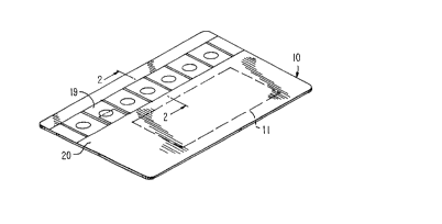
FIG. 1 is a simplified perspective view of a chip card
embodying the present invention in a particular form;
FIG. 2 is an enlarged fragmentary sectional view, not to
scale, taken along the line 2-2 of FIG. 1;
FIG. 3 is a highly simplified diagrammatic view of the
circuitry mounted within the card of FIG. 1;
FIG 4 is a perspective view of a device for reading the
magnetic and optical security portions of the card of FIG. 1; and
FIG. 5 is a block diagram o~ a method of authenticating the
chip card of FIG. 1.
DET~TTlT~n DESCRIPTION
FIG. 1 and 2 show a chip card 10, viz. a plastic (e.g.
polyvinyl chloride) card typically having a thickness of about 30
mils and substantially the same length and width dimensions as an
ordinary present-day credit card, containing externally connectable
electrical circuitry in the form of an integrated circuit or chip
11 mounted within the card, for example being secured between
layers 10a and 10b of the plastic constituting the card, although
the chip may be at least partially exposed at a surface of the
CA 0222921~ 1998-02-10
WO 97/06507 PCT~US96/12948
card. An example o~ such a card is a stored-value card, in which
the amount of money stored may be decremented at off-line termi-
nals.
The chip may, for example, be an integrated circuit of the
type disclosed in the aforementioned U.S. patent No. 4,105,156.
As shown in highly simplified diagrammatic representation in FIG.
3, this chip includes a write once/read only memory (e.g. EPROM)
12, a changeable memory 14, and a processor 16 operatively
connected to memories 12 and 14. The processor is connectable to
an external power supply (not shown) through connector 17, and
input/output connector 18 is also provided for two-way data
communication between the chip and a computer terminal (not shown)
external to the card. These connectors commonly constitute or are
contained in a portion of the chip exposed at the card surface,
although types of connectors not requiring such exposure are also
known and may be used.
First identifying data are permanently written into the read-
only memory 12 for use, as hereinafter explained, in a procedure
for verifying the authenticity of the card. Such data may or may
not be encrypted. The design and operation of the chip 11 are such
as to permit access to the changeable memory 14, and performance
of transactions using the card, only after verification has
occurred.
As a particular feature of the present invention, in the
illustrated embodiment thereof, the plastic substrate of chip card
10 bears a combined machine readable OVD/magnetic stripe, herein
exemplified by a holographic/magnetic stripe 19, mounted on an
external surface 20 thereof so as to be both optically and
magnetically readable by a reading device external to the card.
The holographic/magnetic stripe 19 may be of the type described in
the aforementioned U.S. patent No. 5,336,871. This stripe 19 is
advantageously a laminated composition formed as described in the
aforementioned U.S. patent No. 4,684,795.
Specifically, in this embodiment, a clear plastic carrier 22,
for example a 1/2 to one mil thick clear polyester sheet, is coated
with a release coating of a commercially available clear wax
slipping compound 24. The slipping compound releasably secures a
hologram 26 to the carrier 22 and, upon application of heat,
releases the carrier ~rom the hologram 26. Interposed between the
CA 022292l~ l998-02-lO
WO 97J06507 PCTnUS96/12948
hologram 26 and the slipping compound 24 is one or more coats of
clear scuff 28 and, optionally, a coating of glass beads 30. The
coat(s) of scuff 28 are relatively hard and are conventionally used
to protect magnetic tape after fixation to a substrate. The coat
of glass beads 30, a composition of clear lacquer incorporating
beads typically less than 5 ~m in diameter, acts such that when hit
by light of certain radiation, the resultant radiation can be read
and measured as a further test of the validity of the document.
The hologram 26 is treated, for example with methyl ethyl ketone,
to facilitate adhesion of ferrous oxide 32. A high density slurry
of the ferrous oxide 32 is applied to the hologram 26 by a graw re
coater. The ferrous oxide 32 is generally combined with an
adhesive 34 which fixes the particles of ferrous oxide 32 when dry,
and upon later application of heat provides the "glue" by which the
holographic/magnetic stripe 19 permanently adheres to the substrate
(card) 10. The holographic/magnetic stripe 19 is fixed to the card
by a hot stamping process which (1) activates the adhesive 34 and
(2) allows the carrier 22 to be released from the hologram 26 via
the slipping compound 24. The carrier 22, having performed its
function of providing a base upon which to build the holograph-
ic/magnetic stripe, may be removed and discarded.
It will be understood that, in this described embodiment, the
ferrous oxide 32 constitutes a magnetic stripe and the hologram 26
constitutes an optically readable portion. The ferrous oxide 32
stores encoded magnetic data and the hologram 26 stores encoded
optical data. That is to say, as further disclosed in the
aforementioned U.S. patent No. 5,336,871, identifying data are
carried by the holographic/magnetic stripe and are divided into two
sets of data (second and third identifying data) respectively
encoded in holographic form on the hologram 26, and encoded
magnetically on the magnetic stripe constituted of the ferrous
oxide 32. These second and third identifying data are combinable,
e.g. by a swipe reader (as described below) to derive or generate
fourth identifying data for comparison with the first identifying
data encoded in the write once/read only memory of the chip 11 to
verify the authenticity of the card, e.g. at an off-line ATM or
register at which the card is presented for the purpose of
obtaining cash or merchandise.
CA 0222921~ 1998-02-10
W 097/06507 PCTrUS96/12948
The hologram 26 may configured in any suitable (e.g. known)
machine-readable arrangement for relin~uishing the optical
information, such as the arrangements specifically described in the
aforementioned U.S. patent No. 5,336,871. Preferably in at least
some instances, the optical data may be encoded on the hologram in
the manner disclosed in the aforementioned U.S. patent No.
5,432,329, i.e., as a machine-readable holographic code of the type
described in that patent, for example, a bar code, image plane
holographic pattern, or out of focus holographic pattern, in
combination with an optical clock. By way of illustration, in an
advantageous specific embodiment the hologram may have a holograph-
ically generated off-axis bar code invisible to the naked eye and
readable by a machine reader that will not read an attempted
simulation of a bar code in any other form.
While, as stated, the magnetic and optical data are very
preferably encoded in a stripe 19 comprising a hologram superim-
posed on a magnetic stripe, the hologram and magnetic stripe may
be applied to separate surface portions of the card, as also
explained in the aforementioned U.S. patent No. 5,336,871. There
is, however, an added security advantage in using a superimposed
holographic/magnetic stripe, manufactured in such a way as to
preclude the criminal from using a regular magnetic tape and then
hot-stamping a holographic foil upon it.
An illustrative swipe reader 36 for use with the card 10 is
shown, in somewhat simplified form, in FIG. 4. This swipe reader
is generally of the type described in the aforementioned U.S.
patent N o. 5,336,871, and includes a case 38 which defines an
integral document slot 40 which extends along the right hand side
of the cover 42. The cover 42 defines the side walls as well as
the bottom wall of the slot 40. A magnetic read head 44 is mounted
in an aperture in one of the side walls for detecting magnetic data
encoded on a document's holographic/magnetic stripe 19 as the
document is swiped past the magnetic read head 44. An optical data
reader 46 is mounted in another aperture in one of the side walls
for detecting optical data encoded on a document's holograph-
ic/magnetic stripe 19 as the document is swiped past the optical
data reader 46. The electronic outputs of the magnetic read head
44 and the optical data reader 46 are sent to circuitry 48 for
processing as described in greater detail with reference to FIG.
CA 0222921~ 1998-02-10
WO 97/06507 PCTAUS9~12948
5. The swipe reader 36 also includes a keypad 50 for manual data
input, a display 52 for presenting data, and a data link 54 for
connecting the swipe reader to a local terminal computer 56.
Unlike the swipe reader described in patent No. 5,336,871, the
downstream end 58 of the document slot 40 may be closed, to serve
as a stop for positioning the card after it passes the magnetic and
optical reading elements, and connectors indicated diagrammatically
at 60 and 62 may be mounted in a side wall of the slot to interact
with the power supply connector 17 and input/output connector 18
of the chip 11 when the card is so positioned, thereby to energize
the chip and to provide data exchange through link 54 between the
chip and the local terminal computer. It will be appreciated that
the apparatus of FIG 4 is merely exemplary of terminals with which
the card 10 may be used.
The operation of the card, and the function of the security
elements thereof, may now be readily explained. Stated broadly,
the hologram and the magnetic stripe each contains a separate data
set (second and third identifying data, respectively). Each data
set or identifying data may constitute a digit or a sequence or
string of digits, as may the first identifying data encoded in the
write once/read only memory of the chip. The two sets respectively
encoded on the hologram and the magnetic stripe are combinable to
create an algorithm; thus, the process of reading the holograph-
ic/magnetic stripe is bifurcated, with the hologram and magnetic
stripe each contributing a portion of the algorithm, which is then
communicated to the chip and compared with the algorithm already
stored in the write once/read only memory of the chip 10. The chip
is programmed not to permit a transaction to proceed, or to allow
access to its rewritable memory, unless this key (the algorithm
obtained by reading and combining the data sets coded in the
hologram and the magnetic stripe) is presented.
When the card is swiped, a reader that reads both the magnetic
code and the optical code puts together the algorithm, which must
match the algorithm on the chip in order to initiate the instruc-
tions to the chip card. If the reader does not read an optical
signal and the magnetic number and compute the algorithm which is
also written permanently to the chip card, the transaction is not
allowed.
CA 0222921~ 1998-02-lO
W O 97/06~07 PCTrUS96/12948
In this way, the present invention provides security of access
to the value or other information inside the chip. In the
described method and device, the holographic/magnetic stripe is
coded with what may be characterized as an asymmetric identifica-
tion number, composed of two separate codes which are uniquely
different ~rom each other, respectively carried by the holographic
and magnetic portions of the stripe. The resultant combined code,
or some portion of it, is written to the write once/read only
memory of the chip.
The hologram, in this combination, typically contains a
relatively small, simple part of the code -- e.g., three digits.
In the production of the hologram, by casting with a mold, several
hundred different such three-digit numbers are repetitively formed.
Thus, many cards will have the same holographic number. The second
portion of the card number is permanently coded on the magnetic
stripe, such that when the hologram and magnetic stripe are put
together, their combined numbers constitute or provide a unique
identification number. This number may be encrypted so as to be
determined only by manipulating the combination of the holographi-
cally and magnetically encoded numbers. Also, the data set written
on the write once/read only memory of the chip may or may not be
encrypted.
Illustratively, in an embodiment of the present invention, a
unique random number written to a write once/read only memory in
the chip as described in the aforementioned U.S. patent No.
4,105,156 at the point of manufacture serves as one tumbler in the
"lock" provided by the security system of the invention. The
combined holographically and magnetically coded numbers are used
as another tumbler. The encrypted multiplication or assembly of
the two is used as the final tumbler which, when written and
compared, will ensure that the proper chip is on the proper card
and authenticate the transaction.
In the aforementioned patent No. 4,105,156, a protective code
in the ~orm of a random number is entered during manufacture of the
card into a first memory which is chargeable only once and is
available only within the card. As employed in embodiments of the
present invention, the algorithm is read from the holograph-
ic/magnetic stripe and entered into the card wherein it is compared
internally with the stored protective code for identity; and
CA 0222921~ 1998-02-10
w o 97/06~07 PCT~US96112948
11
responsive to a positive result of such comparison, a release
signal is produced by the processing unit of the card for further
processing of the card.
By way of specific illustration, in the security system of the
invention as in that of the aforementioned patent No. 5,336,871,
a check digit, of which there are a number of versions, commonly
called Modulus (or MOD) 9, 10, 11 or 12, may be used. All check
digit schemes are based upon the manipulation of a base number
multiplying, dividing, adding them together so that by the addition
of a single number at the end of the base string of numbers, the
correctness or authenticity of the base number is verified. Thus
a serial number as in 12345 would have added to itself a check
digit number which would be from 0 to 9 depending upon the modulus
calculation, i.e. 123453. If there were a juxtaposition or
transposing error in the number 123453, i.e., 132453 the check
digit number would no longer be the numeral 3 and a flag or error
would be noticed.
As an example of such operation, the third identifying data,
encoded magnetically on the holographic/magnetic stripe 19, may be
the string of numbers 123458. The second identifying data, encoded
in the hologram (optically readable portion) of the stripe 19, may
be the single number 4. The swipe reader combines these two data
sets to produce a string of digits 4123458. In this string of
digits, "8" is the correct check digit for 412345. Intelligent
circuitry 48 in the swipe reader, presented with the combined
string 4123458, will recognize that 8 is the correct check digit
in this case and will allow the security operation to proceed to
the next stage. If, however, the number encoded on the holographic
portion of stripe 19 were a number other than 4, or were missing,
the swipe reader circuitry 48 would deny further access.
The first identifying data, encoded on the write once/read
only chip memory, may be 123458. If the swipe reader verifies the
combined optical and magnetic readings from the stripe, it is
programmed to transmit the number string 123458 to the chip as the
fourth identifying data. The chip internally compares this number
string with that encoded in its write once/read only memory and,
finding the first and fourth identifying data to be identical,
allows the transaction to proceed. If, however, some other number
string were transmitted by the swipe reader to the chip, the chip
CA 022292l~ l998-02-lO
W O 97/06S07 PCT~US96/12948
12
processor would find lack of identity between the first and fourth
identifying data and would deny further access. The swipe reader
and/or the chip could further be programmed, after a limited number
of retries of either verifying step, to cause the terminal to send
an electrical pulse that would disable the card, e.g. by acting on
one or more disabling devices such as fuses (not shown) incorporat-
ed in known manner in the chip circuitry.
This operation is illustrated diagrammatically in FIG. 5.
When a cardholder presents the card 10 to an off-line ATM incorpo-
rating a swipe reader as shown in FIG. 4 for the purpose of making
a cash withdrawal, and swipes the card along the slot, the swipe
reader circuitry 48 reads the hologram of the stripe 19 as
indicated at 66, reads the magnetic portion of the stripe as
indicated at 68, combines them as indicated at 70, and as indicated
at 72, determines whether the card as thus far examined is valid
(i.e., in the above example, whether the check digit 8 is correct
~or the combined number string 412345 derived from the separately
encoded second and third identifying data). If the reader finds
the data invalid, it retries or incapacitates the card. If the
reader finds the data valid, as indicated at 74, it transmits a
portion of the string (123458) as fourth identi~ying data to the
chip 11 for further verification.
The processor of the chip then reads the first identifying
data encoded on the write once/read only memory of the chip as
indicated at 76, compares that number string with the transmitted
fourth identifying data from the swipe reader as indicated at 78,
and determines whether the two are identical as indicated at 80.
I~ the chip processor finds nonidentity, it retries or incapaci-
tates the card; if it determines that the compared number strings
are identical, it permits the transaction to proceed. The
cardholder may key into the swipe reader the amount of cash
desired, and if the card bears at least this amount, as determined
from the changeable memory of the chip, the ATM delivers that sum
in cash and debits the changeable memory o~ the chip by the same
amount, also recording the transaction thereon.
In one modification of the method and article of the inven-
tion, the magnetic stripe is omitted, and the externally readable
hologram 26 is used alone, i.e., mounted on the exterior of the
card. The hologram and the chip memory 12 in such case separately
CA 0222921~ 1998-02-lO
WO 97/06507 PCTAUS96/12948 13
contain data sets that may be combined (for example, in the same
manner as the respective data sets of the hologram and the magnetic
stripe in the procedure of the aforementioned U.S. patent No.
5,336,871) by the chip to verify authenticity and permit or prevent
a desired transaction using the card.
If the magnetic stripe is omitted, and only a hologram is
J used, bearing a machine readable holographic number, the optical
number hidden in the hologram is read and the result written to the
chip. Thereafter, when the chip card is used the reader must see
and compare the optical number with the number on the chip in order
to initiate a transaction.
An advantage of the invention, in all of the above-described
embodiments, is that it requires knowledge o~ two very different
technologies -- that of computers, and optics -- for successful
counterfeiting. Unless a correctly coded hologram (or other
machine readable OVD) is matched with a correctly written chip
read-only memory in the same card, use of the card will be blocked.
It is to be understood that the invention is not limited to
the features and embodiments herein specifically set forth, but may
be carried out in other ways without departure from its spirit.