Note: Descriptions are shown in the official language in which they were submitted.
CA 02229567 2000-07-25
PATENT APPLICATION
Attorney Docket No. D/9624402
INORGANIC COATED DEVELOPMENT ELECTRODES
AND METHODS THEREOF
BACKGROUND OF THE INVENTION
The present invention relates to methods, processes and apparatii for
development
of images, and more specifically, to electrode members for use in a developer
unit in
electrophotographic printing machines. Specifically, the present invention
relates to
methods and apparatii in which at least a portion of a development unit
electrode member
is coated with a coating material, and in embodiments, a low surface energy
coating
material. In embodiments, electrode member history, damping and/or toner
accumulation
is controlled or reduced.
Generally, the process of electrophotographic printing includes charging a
photoconductive member to a substantially uniform potential so as to sensitize
the
25
1
CA 02229567 1998-02-12
photoconductive member thereof. The charged portion of the photoconductive
member is exposed to a light image of an original document being reproduced.
This
records an electrostatic latent image on the photoconductive member. After the
electrostatic latent image is recorded on the photoconductive member, the
latent
s image is developed by bringing a developer material into contact therewith.
Two
component and single component developer materials are commonly used. A
typical two component developer material comprises magnetic carrier granules
having toner particles adhering triboelectrically thereto. A single component
developer material typically comprises toner particles. Toner particles are
attracted
io to the latent image forming a toner powder image on the photoconductive
member.
The toner powder image is subsequently transferred to a copy sheet. Finally,
the
toner powder image is heated to permanently fuse it to the copy sheet in image
configuration.
One type of single component development system is a scavengeless
is development system that uses a donor roll for transporting charged toner to
the
development zone. At least one, and preferably a plurality of electrode
members
are closely spaced to the donor roll in the development zone. An AC voltage is
applied to the electrode members forming a toner cloud in the development
zone.
The electrostatic fields generated by the latent image attract toner from the
toner
2o cloud to develop the latent image.
Another type of two component development system is a hybrid
scavengeless development system which employs a magnetic brush developer
roller for transporting carrier having toner adhering triboelectrically
thereto. A donor
roll is used in this configuration also to transport charged toner to the
development
2s zone. The donor roll and magnetic roller are electrically biased relative
to one
another. Toner is attracted to the donor roll from the magnetic roll. The
electrically
biased electrode members detach the toner from the donor roll forming a toner
powder cloud in the development zone, and the latent image attracts the toner
particles thereto. In this way, the latent image recorded on the
photoconductive
3o member is developed with toner particles.
2
CA 02229567 2000-07-25
Various types of development Systems have hereinbefore been used as
illustrated
by the following disclosures.
U.S. Patent No. 4,868,600 to Hays et al. describes an apparatus wherein a
donor roll transports toner to a region opposed from a surface on which a
latent image is
recorded. A pair of electrode members are positioned in the space between the
latent
image surface and the donor roll and are electrically biased to detach toner
from the donor
roll to form a toner cloud. Detached toner from the cloud develops the latent
image.
U.S. Patent No. 4,984,019, to Folkins discloses a developer unit having a
donor
roll with electrode members disposed adjacent thereto in a development zone. A
magnetic
roller transports developer material to the donor roll. Toner particles are
attracted from the
magnetic roller to the donor roller. When the developer unit is inactivated,
the electrode
members are vibrated to remove contaminants therefrom.
U.S. Patent 5,124,749 to Bares discloses an apparatus in which a donor roll
advances toner to an electrostatic latent image recorded on a photoconductive
member
wherein a plurality of electrode wires are positioned in the space between the
donor roll
and the photoconductive member. The wires are electrically biased to detach
the toner
from the donor roll so as to form a toner cloud in the space between the
electrode wires
and the photoconductive member. The powder cloud develops the latent image. A
damping material is coated on a portion of the electrode wires at the position
of attachment
to the electrode supporting members for the purpose of damping vibration of
the electrode
wires.
U.S. Patents 5,300,339 and 5,448,342 both to Hays et al. disclose a coated
toner
transport roll containing a core with a coating thereover.
U.S. Patent 5,172,170 to Hays et al. discloses an apparatus in which a donor
30
3
CA 02229567 1998-02-12
roll advances toner to an electrostatic latent image recorded on a
photoconductive
member. The donor roll includes a dielectric layer disposed about the
circumferential surface of the roll between adjacent grooves.
Primarily because the adhesion force of the toner particles is greater than
the
stripping force generated by the electric field of the electrode members in
the
development zone, a problem results in that toner tends to build up on the
electrode
members. Accumulation of toner particles on the wire member causes non-uniform
development of the latent image, resulting in print defects. The problem is
aggravated by toner fines and any toner components, such as high molecular
to weight, crosslinked and/or branched components, and the voltage breakdown
between the wire member and the donor roll.
One specific example of toner contamination results upon development of a
document having solid areas which require a large concentration of toner to be
deposited at a particular position on the latent image. The areas of the
electrode
t5 member corresponding to the high throughput or high toner concentration
areas
tend to include higher or lower accumulation of toner because of this
differing
exposure to toner throughput. When the printer subsequently attempts to
develop
another, different image, the toner accumulation on the electrode member will
lead
to differential development of the newly developed image corresp8nding to the
2o areas of greater or lesser toner accumulation on the electrode members. The
result
is a darkened or lightened band in the position corresponding to the solid
area of
the previous image. This is particularly evident in areas of intermediate
density,
since these are the areas most sensitive to differences in development. These
particular image defects caused by toner accumulation on the electrode wires
at the
2s development zone are referred to as wire history. Figure 5 contains an
illustration
of wire contamination and wire history. Wire contamination results when fused
toner forms between the electrode member and donor member due to toner fines
and any toner components, such as high molecular weight, crosslinked and/or
branched components, and the voltage breakdown between the wire member and
4
CA 02229567 2000-07-25
the donor roll. Wire history is a change in developability due to toner or
toner components
sticking to the top of the electrode member.
Accordingly, there is a specific need for electrode members in the development
zone of a development unit of an electrophotographic printing machine which
provide for
a decreased tendency for toner accumulation in order to decrease wire history
and wire
contamination, especially at high throughput areas, and decreasing the
production of
unwanted surface static charges from which contaminants may not release. One
possible
solution is to change the electrical properties of the wire. However, attempts
at decreasing
toner build-up on the development wire by changing the electrical properties
thereof, may
result in an interference with the function of the wire and its ability to
produce the
formation of the toner powder cloud. Therefore, there is a specific need for
electrode
members which have a decreased tendency to accumulate toner and which also
retain their
electrical properties in order to prevent interference with the functioning
thereof. There is
an additional need for electrode members which have superior mechanical
properties
including durability against severe wear the electrode member receives when it
is
repeatedly brought into contact with tough rotating donor member surfaces.
SUMMARY OF THE INVENTION
Examples of objects of the present invention include:
It is an object of an aspect of the present invention to provide an apparatus
for
reducing toner accumulation of electrode members in the development zone of a
developing unit in an electrophotographic printing apparatus with many of the
advantages
indicated herein.
Another object of an aspect of the present invention is to provide an
apparatus for
reducing toner adhesion to electrode members.
It is another object of an aspect of the present invention to provide an
apparatus
comprising electrode members having a lower surface energy.
It is yet another object of an aspect of the present invention to provide an
apparatus
comprising electrode members having increased mechanical strength.
5
CA 02229567 2000-07-25
Still yet another object of an aspect of the present invention is to provide
an
apparatus comprising electrode members which have superior electrical
properties.
A further object of an aspect of the present invention is to provide an
apparatus
comprising electrode members which have smooth surfaces.
Many of the above objects have been met by the present invention, in
embodiments, which includes: an apparatus for developing a latent image
recorded on a
surface, comprising: wire supports; a donor member spaced from the surface and
being
adapted to transport toner to a region opposed from the surface; an electrode
member
positioned in the space between the surface and the donor member, the
electrode member
being closely spaced from the donor member and being electrically biased to
detach toner
from the donor member thereby enabling the formation of a toner cloud in the
space
between the electrode member and the surface with detached toner from the
toner cloud
developing the latent image, wherein opposed end regions of the electrode
member are
attached to wire supports adapted to support the opposed end regions of said
electrode
member; and an inorganic coating on at least a portion of nonattached regions
of said
electrode member.
Embodiments further include: an electrophotographic process comprising:
a) forming an electrostatic latent image on a charge-retentive surface; b)
applying
toner in the form of a toner cloud to said latent image to form a developed
image on said
charge retentive surface, wherein said toner is applied using a development
apparatus
comprising wire supports; a donor member spaced from the surface and being
adapted to
transport toner to a region opposed from the surface; an electrode member
positioned in
the space between the surface and said donor member, said electrode member
being
closely spaced from said donor member and being electrically biased to detach
toner from
said donor member thereby enabling the formation of a toner cloud in the space
between
said electrode member and the surface with detached toner from the toner cloud
developing the latent image, wherein opposed end regions of said electrode
member are
attached to said wire supports adapted to support the opposed end regions of
said electrode
member;
6
CA 02229567 2000-07-25
and an inorganic coating on at least a portion of nonattached regions of said
electrode
member; c) transferring the toner image from said charge-retentive surface to
a substrate;
and d) fixing said toner image to said substrate.
The present invention provides electrode members which, in embodiments, have a
decreased tendency to accumulate toner and which also, in embodiments, retain
their
electrical properties in order to prevent interference with the functioning
thereof. The
present invention further provides electrode members which, in embodiments,
have
superior mechanical properties including durability against severe wear the
electrode
member receives when it is repeatedly brought into contact with tough rotating
donor roll
surfaces.
BRIEF DESCRIPTION OF THE DRAWINGS
The above aspects of the present invention will become apparent as the
following
description proceeds upon reference to the drawings in which:
Figure 1 is a schematic illustration of an embodiment of a development
apparatus
useful in an electrophotographic printing machine.
Figure 2 is an enlarged, schematic illustration of a donor roll and electrode
member
representing an embodiment of the present invention.
Figure 3 is a fragmentary schematic illustration of a development housing
comprising a donor roll and an electrode member from a different angle than as
shown in
Figure 2.
Figure 4 is an enlarged, schematic illustration of an electrode member
supported by
mounting means in an embodiment of the present invention.
Figure 5 is an illustration of wire contamination and wire history.
DETAILED DESCRIPTION
For a general understanding of the features of the present invention, a
description
thereof will be made with reference to the drawings.
Figure 1 shows a development apparatus used in an electrophotographic printing
machine such as that illustrated and described in U.S. Patent 5,124,749.
7
CA 02229567 2000-07-25
This patent describes the details of the main components of an
electrophotographic
printing machine and how these components interact. The present application
will
concentrate on the development unit of the electrophotographic printing
machine.
Specifically, after an electrostatic latent image has been recorded on a
photoconductive
surface, a photoreceptor belt advances the latent image to the development
station. At the
development station, a developer unit develops the latent image recorded on
the
photoconducti ve surface.
Referring now to Figure 1, in a preferred embodiment of the invention,
developer
unit 38 develops the latent image recorded on the photoconductive surface 10.
Preferably,
developer unit 38 includes donor roller 40 and electrode member or members 42.
Electrode members 42 are electrically biased relative to donor roll 40 to
detach toner
therefrom so as to form a tonerpowder cloud in the gap between the donor roll
40 and
photoconductive surface 10. The latent image attracts toner particles from the
toner
powder cloud forming a toner powder image thereon. Donor roller 40 is mounted,
at least
partially, in the chamber of developer housing 44. The chamber in developer
housing 44
stores a supply of developer material. The developer material is a two
component
developer material of at least carrier granules having toner particles
adhering
triboelectrically thereto. A magnetic roller 46 disposed interior of the
chamber of housing
44 conveys the developer material to the donor roller 40. The magnetic roller
46 is
electrically biased relative to the donor roller so that the toner particles
are attracted from
the magnetic roller to the donor roller.
More specifically, developer unit 38 includes a housing 44 defining a chamber
76
for storing a supply of two component (toner and carrier) developer material
therein.
Donor roller 40, electrode members 42 and magnetic roller 46 are mounted in
chamber 76
of housing 44. The donor roller can be rotated in either the 'with' or
'against' direction
relative to the direction of motion of belt 10. In Figure 1, donor roller 40
is shown rotating
in the direction of arrow 68. Similarly, the magnetic roller can be rotated in
either the
'with' or 'against' direction relative to the direction
8
CA 02229567 1998-02-12
of motion of belt 10. In Figure 1, magnetic roller 46 is shown rotating in the
direction
of arrow 92. Donor roller 40 is preferably made from anodized aluminum or
ceramic.
Developer unit 38 also has electrode members 42 which are disposed in the
space between the belt 10 and donor roller 40. A pair of electrode members are
shown extending in a direction substantially parallel to the longitudinal axis
of the
donor roller. The electrode members are made from of one or more thin (i.e.,
50 to
100 p,m in diameter) stainless steel or tungsten electrode members which are
closely spaced from donor roller 40. The distance between the electrode
members
io and the donor roller is from about 5 to about 35 p.m, preferably about 10
to about 25
~m or the thickness of the toner layer on the donor roll. The electrode
members are
self-spaced from the donor roller by the thickness of the toner on the donor
roller.
To this end, the extremities of the electrode members supported by the tops of
end
bearing blocks also support the donor roller for rotation. The electrode
member
is extremities are attached so that they are slightly above a tangent to the
surface,
including toner layer, of the donor structure. Mounting the electrode members
in
such a manner makes them insensitive to roll run-out due to their self-
spacing.
As illustrated in Figure 1, an alternating electrical bias is applied to the
electrode members by an AC voltage source 78. The applied AC establishes an
2o alternating electrostatic field between the electrode members and the donor
roller is
effective in detaching toner from the photoconductive member of the donor
roller
and forming a toner cloud about the electrode members, the height of the cloud
being such as not to be substantially in contact with the belt 10. The
magnitude of
the AC voltage is relatively low and is in the order of 200 to 500 volts peak
at a
2s frequency ranging from about 9 kHz to about 15 kHz. A DC bias supply 80
which
applies approximately 300 volts to donor roller 40 establishes an
electrostatic field
between photoconductive member of belt 10 and donor roller 40 for attracting
the
detached toner particles from the cloud surrounding the electrode members to
the
latent image recorded on the photoconductive member. At a spacing ranging from
9
CA 02229567 1998-02-12 '
about 0.001 p,m to about 45 ~.m between the electrode members and donor
roller,
an applied voltage of 200 to 500 volts produces a relatively large
electrostatic field
without risk of air breakdown. A cleaning blade 82 strips all of the toner
from donor
roller 40 after development so that magnetic roller 46 meters fresh toner to a
clean
donor roller. Magnetic roller 46 meters a constant quantity of toner having a
substantially constant charge onto donor roller 40. This insures that the
donor roller
provides a constant amount of toner having a substantially constant charge in
the
development gap. In lieu of using a cleaning blade, the combination of donor
roller
spacing, i.e., spacing between the donor roller and the magnetic roller, the
io compressed pile height of the developer material on the magnetic roller,
and the
magnetic properties of the magnetic roller in conjunction with the use of a
conductive, magnetic developer material achieves the deposition of a constant
quantity of toner having a substantially charge on the donor roller. A DC bias
supply 84 which applies approximately 100 volts to magnetic roller 46
establishes
is an electrostatic field between magnetic roller 46 and donor roller 40 so
that an
electrostatic field is established between the donor roller and the magnetic
roller
which causes toner particles to be attracted from the magnetic roller to the
donor
roller. Metering blade 86 is positioned closely adjacent to magnetic roller 46
to
maintain the compressed pile height of the developer material on magnetic
roller 46
2o at the desired level. Magnetic roller 46 includes a non-magnetic tubular
member 88
made preferably from aluminum and having the exterior circumferential surface
thereof roughened. An elongated magnet 90 is positioned interiorly of and
spaced
from the tubular member. The magnet is mounted stationarily. The tubular
member
rotates in the direction of arrow 92 to advance the developer material
adhering
Zs thereto into the nip defined by donor roller 40 and magnetic roller 46.
Toner
particles are attracted from the carrier granules on the magnetic roller to
the donor
roller.
W ith continued reference to Figure 1, an auger, indicated generally by the
reference numeral 94, is located in chamber 76 of housing 44. Auger 94 is
mounted
3o rotatably in chamber 76 to mix and transport developer material. The auger
has
io
CA 02229567 2000-07-25
blades extending spirally outwardly from a shaft. The blades are designed to
advance the
developer material in the axial direction substantially parallel to the
longitudinal axis of
the shaft.
As successive electrostatic latent images are developed, the toner particles
within
the developer material are depleted. A toner dispenser (not shown) stores a
supply of toner
particles which may include toner and carrier particles. The toner dispenser
is in
communication with chamber 76 of housing 44. As the concentration of toner
particles in
the developer material is decreased, fresh toner particles are furnished to
the developer
material in the chamber from the toner dispenser. In an embodiment of the
invention, the
auger in the chamber of the housing mix the fresh toner particles with the
remaining
developer material so that the resultant developer material therein is
substantially uniform
with the concentration of toner particles being optimized. In this way, a
substantially
constant amount of toner particles are in the chamber of the developer housing
with the
toner particles having a constant charge. The developer material in the
chamber of the
developer housing is magnetic and may be electrically conductive. By way of
example, in
an embodiment of the invention wherein the toner includes carrier particles,
the carrier
granules include a ferromagnetic core having a thin layer of magnetite
overcoated with a
non-continuous layer of resinous material. The toner particles may be made
from a
resinous material, such as a vinyl polymer, mixed with a coloring material,
such as
chromogen black. The developer material may comprise from about 90% to about
99% by
weight of carrier and from 10% to about 1 % by weight of toner. However, one
skilled in
the art will recognize that any other suitable developer material may be used.
In an alternative embodiment of the present invention, one component developer
material consisting of toner without carrier may be used. In this
configuration, the
magnetic roller 46 is not present in the developer housing. This embodiment is
described
in more detail in U.S. Patent 4,868,600.
11
CA 02229567 1998-02-12
An embodiment of the developer unit is further depicted in Figure 2. The
developer apparatus 34 comprises an electrode member 42 which is disposed in
the
space between the photoreceptor (not shown in Figure 2) and the donor roll 40.
The electrode 42 can be comprised of one or more thin (i.e., 50 to about 100
pm in
s diameter) tungsten or stainless steel electrode members which are lightly
positioned
at or near the donor structure 40. The electrode member is closely spaced from
the
donor member. The distance between the wires) and the donor is approximately
0.001 to about 45 p.m, and preferably from about 10 to about 25 pm or the
thickness
of the toner layer 43 on the donor roll. The wires as shown in Figure 2 are
self
to spaced from the donor structure by the thickness of the toner on the donor
structure.
The extremities or opposed end regions of the electrode member are supported
by
support members 54 which may also support the donor structure for rotation. In
a
preferred embodiment, the electrode member extremities or opposed end regions
are attached so that they are slightly below a tangent to the surface,
including toner
is layer, of the donor structure. Mounting the electrode members in such a
manner
makes them insensitive to roll runout due to their self-spacing.
In an alternative embodiment to that depicted in Figure 1, the metering blade
86 is replaced by a combined metering and charging blade 86 as shown ~n Figure
3.
The combination metering and charging device may comprise any suitable device
2o for depositing a monolayer of well charged toner onto the donor structure
40. For
example, it may comprise an apparatus such as that described in U.S. Patent
4,459,009, wherein the contact between weakly charged toner particles and a
triboelectrically active coating contained on a charging roller results in
well charged
toner. Other combination metering and charging devices may be employed, for
2s example, a conventional magnetic brush used with two component developer
could
also be used for depositing the toner layer onto the donor structure, or a
donor roller
alone used with one component developer.
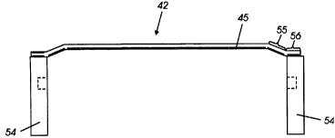
Figure 4 depicts an enlarged view of a preferred embodiment of the electrode
member of the present invention. Electrode wires 45 are positioned inside
electrode
3o member 42. The anchoring portions 55 of the electrode members are the
portions
12
CA 02229567 1998-02-12
of the electrode member which anchor the electrode member to the support
member. The mounting sections 56 of the electrode member are the sections of
the
electrode members between the electrode member and the mounting means 54.
Toner particles are attracted to the electrode members primarily through
s electrostatic attraction. Toner particles adhere to the electrode members
because
the adhesion force of the toner is larger than the stripping force generated
by the
electric field of the electrode member. Generally, the adhesion force between
a
toner particle and an electrode member is represented by the general
expression
Fad = q2/krz + W, wherein Fad is the force of adhesion, q is the charge on the
toner
to particle, k is the effective dielectric constant of the toner and any
dielectric coating,
and r is the separation of the particle from its image charge within the wire
which
depends on the thickness, dielectric constant, and conductivity of the
coating.
Element W is the force of adhesion due to short range adhesion forces such as
van
der Waals and capillary forces. The force necessary to strip or remove
particles
is from the electrode member is supplied by the electric field of the wire
during half of
its AC period, qE, plus effective forces resulting from mechanical motion of
the
electrode member and from bombardment of the wire by toner in the cloud. Since
the adhesion force is quadratic in q, adhesion forces will be larger than
stripping
forces for sufficiently high values of q.
2o Figure 5 contains an illustration of wire contamination and wire history. A
photoreceptor 1 is positioned near wire 4 and contains an undeveloped image 6
which is subsequently developed by toner originating from donor member 3. Wire
contamination occurs when fused toner 5 forms between the wire 4 and donor
member 3. The problem is aggravated by toner fines and any toner components,
25 such as high molecular weight, crosslinked and/or branched components, and
the
voltage breakdown between the wire member and the donor roll. Wire history is
a
change in developability due to toner 2 or toner components sticking to the
top of
the wire 4, the top of the wire being the part of the wire facing the
photoreceptor.
In order to prevent the toner defects associated with wire contamination and
3o wire history, the electrical properties of the electrode member can be
changed,
13
CA 02229567 1998-02-12
thereby changing the adhesion forces in relation to the stripping forces.
However,
such changes in the electrical properties of the electrode member may
adversely
affect the ability of the electrode member to adequately provide a toner
cloud, which
is essential for developing a latent image. The present invention is directed
to an
s apparatus for reducing the unacceptable accumulation of toner on the
electrode
member while maintaining the desired electrical and mechanical properties of
the
electrode member. The electrode member of the present invention is coated with
a
material coating that reduces the significant attraction of toner particles to
the
electrode member which may result in toner accumulation. However, the material
to coating does not adversely interfere with the mechanical or electrical
properties of
the electrode member. Materials having these qualities include materials with
a low
surface energy.
The low surface energy material decreases the accumulation of toner by
assuring electrical continuity for charging the wires and eliminates the
possibility of
15 charge build-up. In addition, such low surface energy materials as
described herein
do not interfere with the electrical properties of the electrode member and do
not
adversely affect the electrode's ability to produce a toner powder cloud.
Moreover,
the electrode member maintains its tough mechanical properties, allowing the
electrode member to remain durable against the severe wear the electrode
member
2o receives when it is repeatedly brought into contact with tough, rotating
donor roll
surfaces. Also, the electrode member maintains a "smooth" surface after the
coating is applied. A smooth surface includes surfaces having a surface
roughness
of less than about 5 microns, preferably from about 0.01 to about 1 micron.
Examples of suitable low surface energy electrode coating materials include
Zs both organic materials and inorganic materials. It is preferred that the
inorganic
material possess the characteristics of low surface energy, high hardness,
very low
or no porosity, smooth surface characteristics, low friction and high wear
resistance
to enable the wire to withstand numerous cycling for every day use in an
electrophotographic apparatus. Examples of suitable inorganic materials
3o possessing the above characteristics include ceramics, borosilicate
glasses,
14
CA 02229567 1998-02-12
diamond and diamond like compounds, silicone hard coatings, molybdenum
silicide,
and derivatives thereof. Examples of ceramics having little or no porosity,
include
boron nitride, zirconium oxide, titanium carbide, silicon carbide, titanium
nitride,
zirconium diboride, yettrium oxide, glass ceramic (having about 75 percent by
weight silica) and the like. Suitable ceramic coating materials are available
as
stable dispersions from ZYP Coatings Co. of Oak Ridge, Tennessee. Heat
resistant
glass such as, for example, borosilicate glasses, are also suitable inorganic
materials and possess the above characteristics. Glass coated wires are
commercially available from AMTX Company of Canandaguia, NY and Pegasus of
to Springfield, MA. Diamond and diamond derivative coatings including low
grade
diamonds such as, for example, bort and carbonado, are also suitable low
surface
inorganics and commercially available examples include "Dylyn Coating" by
Advanced Refractory Technologies of Buffalo, New York which is a self
compensating interpenetrating network of carbon, hydrogen, silicone and
oxygen.
t5 Another suitable low surface energy inorganic material is molybdenum
silicide
(MoSi2) and its combination with silica, both forms of which are commercially
available as stable dispersions from ZYP Coatings of Oak Ridge, Tennessee.
Other
suitable low surface energy inorganic materials include hard silicone coatings
such
as, for example, silanes and siloxanes, which can be deposited on the wire
surface
2o by lon Beam Assisted Deposition method, thereby forming inorganic hard
silicone
coatings. The details of this technique are published in the Journal of
Materials
Research, vol. 6, page 871, 1991, the disclosure of which is hereby
incorporated by
reference in its entirety.
A filler such as an electrically conductive filler, may be added to the
material
25 coating in the amount of from about 5 to about 35 percent by weight of
total solids,
preferably from about 15 to about 20 percent by weight of total solids. Total
solids
herein include the amount of filler and inorganic solid material, catalyst,
and any
additives. Examples of electrically conductive fillers include metal oxides
such as
tin oxide, titanium oxide, zirconium oxide. Another preferred filler is carbon
black,
3o graphite or the like, with surface treatment of compounds such as for
example,
is
CA 02229567 2000-07-25
siloxane, silane, fluorine or the like. Specifically preferred treated carbon
blacks include
fluorinated carbons such as those described in U.S. Patent 5,849,399.
The low surface energy inorganic coating material is preferably present in an
amount of from about 5 to about 95 percent by weight of total solids, and
preferably from
about 10 to about 40 percent by weight of total solids. Total solids as used
herein, refers to
the total amount by weight of inorganic coating material, fillers, and
additives contained in
the coating solution.
The volume resistivity of the coated electrode is for example from about 10-
I° to
about 1'~ ohm-cm, and preferably from 10-5 to 10-1 ohm-cm. The surface
roughness is less
than about 5 microns and preferably from about 0.01 to about 1 micron.
In a preferred embodiment of the invention, the material coating is coated
over at
least a portion of the nonattached regions of the electrode member. The
nonattached
region of the electrode member is the entire outer surface region of the
electrode minus the
region where the electrode is attached to the mounting means 54 and minus the
anchoring
area (55 in Figure 4). It is preferred that the coating cover the portion of
the electrode
member which is adjacent to the donor roll. In another preferred embodiment of
the
invention, the material coating is coated in an entire area of the electrode
member located
in a central portion of the electrode member and extending to an area adjacent
to the
nonattached portion of the electrode member. This area includes the entire
surface of the
electrode member minus the anchoring area (55 in Figure 4). In an alternative
embodiment, the entire length of the electrode member is coated with the
material coating,
including the anchoring area 55 and mounting area 56. In embodiments, at least
a portion
refers to the non-attached region being coated, or from about 10 to about 90
percent of the
electrode member.
Toner can accumulate anywhere along the electrode member, but it will not
adversely affect development unless it accumulates in the length of the
electrode
16
CA 02229567 2000-07-25
member near to the donor roll or on the length closest to the photoreceptor.
Therefore, it is
preferred that the material coating cover the electrode member along the
entire length
corresponding to the donor roll, and on the entire length corresponding to the
photoreceptor.
The material coating may be deposited on at least a portion of the electrode
member by any suitable, known method. These deposition methods include liquid
and
powder coating, dip and spray coating, and ion beam assisted and RF plasma
deposition.
In a preferred deposition method, the material coating is coated on the
electrode member
by dip coating. With silicone materials, it is preferred to apply these
coatings by ion beam
assisted deposition. After coating, the inorganic coating is preferably air
dried and cured at
a temperature suitable for curing the specific inorganic material. Curing
temperatures
range from about 400 to about 1400°C, and preferably from about 600 to
about 1200°C.
The average thickness of the coating is from about 1 to about 30 ~,m thick,
and
preferably from about 2 to about 10 pm thick. If the coating is applied to
only a portion of
the electrode member, the thickness of the coating may or may not taper off at
points
farthest from the midpoint of the electrode member. Therefore, the thickness
of the coating
may decrease at points farther away from the midpoint of the electrode.
The electrode members of the present invention, the embodiments of which have
been described herein exhibit superior performance in terms wear resistance
and decreased
accumulation of toner on the surface of the electrode member, while also
maintaining
electrical properties which stimulate production of powder cloud development
without
charge build-up. In addition, the electrode members herein exhibit superior
mechanical
properties such as durability against donor roll surfaces which are normally
made of tough
materials such as ceramics.
30
17
CA 02229567 1998-02-12
The following Examples further define and describe embodiments of the
present invention. Unless otherwise indicated, all parts and percentages are
by
weight.
ig
CA 02229567 1998-02-12
EXAMPLES
EXAMPLE 1
Preparation of wire to be coated
A stainless steel wire of about 3 mil thickness is preferably cleaned to
remove obvious contaminants.
A dip coating apparatus with a 1 inch (diameter) by 15 inches (length) glass
cylinder sealed at one end to hold the liquid coating material can be used for
dip
s coating the wire. A cable attached to a Bodine Electric Company type NSH-12R
motor is used to raise and lower a wire support holder that keeps the wire
taut
during the coating process. The dip and withdraw rate of the wire holder into
and
out of the coating solution can be regulated by a motor control device from
B&B
Motors & Control Corporation, (NOVA PD DC motor speed control). After coating,
a
to motor driven device is used to twirl the wire around its axis while it
receives external
heating to allow for controlled solvent evaporation. When the coating is dry
and/or
non-flowable, the coated wire can be heated in a flow through oven using a
time and
temperature schedule to complete either drying or cure/ post cure of the
coating.
The general procedure may include: (A) cleaning and degreasing the wire
15 with an appropriate solvent, for example, acetone, alcohol or water, and
roughened
if necessary by, for example, sand paper; (B) the coating material may be
adjusted
to the proper viscosity and solids content by adding solids or solvent to the
solution;
and (C) the wire is dipped into and withdrawn from the coating solution, dried
and
cured/post cured, if necessary, and dipped again, if required. The coating
thickness
2o and uniformity are a function of withdrawal rate and solution viscosity,
(solids
content in most solvent based systems) and a drying schedule consistent with
the
uniform solidification of the coating.
19
CA 02229567 1998-02-12
EXAMPLES
Preparation of inorganic coatin4 solutions
EXAMPLE 1
A stainless steel wire of 3 mil thickness can be cleaned to remove obvious
contaminants. High purity titanium nitride (TiN) dispersion Type "TN" obtained
from
ZYP Coatings Inc., of Oak Ridge, TN, having 75% solids content is then added
to
the coating tank of the dip coater. This coating can be applied using
conventional
dip coating method as described in Example 1. The coatings can then be air
dried
and cured at 400°C for 12 hours. The resulting coating surface can then
be hand
polished through a rubbing action by using a back and forth wiping motion.
EXAMPLE 2
A dispersion containing zirconium diboride obtained from ZYP Coatings Inc,
of Oak Ridge, TN as Type "ZB-MOD" having 58% solids contents can be used as an
io inorganic coating solution. This coating can be applied using conventional
dip
coating method as described in Example 1. The coatings can then be air dried
and
cured at 1,200-1,600°C.
EXAMPLE 3
A dispersion of molybdenum disilicide obtained from ZYP Coatings Inc, of
Oak Ridge, TN sold as Type "MS" having about 50% solids can be used as an
is inorganic coating. This coating can be applied using conventional dip
coating
method as described in Example 1. The coatings can then be air dried and cured
at
1,200-1,600°C.
CA 02229567 1998-02-12
EXAMPLE 4
A dispersion of boron nitride obtained from ZYP Coatings Inc, of Oak Ridge,
TN sold as Type "BN-MOD" and having about 25 % solids can be used as an
inorganic coating. This coating can be applied using conventional dip coating
method as described in Example 1. The coatings can then be air dried and cured
at
700-1,000°C.
EXAMPLE 5
A dispersion of titanium carbide obtained from ZYP Coatings Inc, of Oak
Ridge, TN sold as Type "T" and having about 45% solids can be used as an
inorganic coating. This coating can be applied using conventional dip coating
method as described in Example 1. The coatings can then be air dried and cured
at
700-900°C.
EXAMPLE 6
A steel wire can be coated by Advanced Refractory Technology of Buffalo,
NY with self compensating interpenetrating network of carbon, hydrogen,
silicone
and oxygen which is commercially called "Dylyn". The thickness of the coating
is
estimated to be from about 1 to about 3 microns, very smooth and relatively
hard.
is The electrical conductivity is estimated to be about 10-9 ohm-cm.
While the invention has been described in detail with reference to specific
and preferred embodiments, it will be appreciated that various modifications
and
variations will be apparent to the artisan. All such modifications and
embodiments
as may readily occur to one skilled in the art are intended to be within the
scope of
2o the appended claims.
21