Note: Descriptions are shown in the official language in which they were submitted.
CA 02229~70 l998-02-l2
OPTICAL COUPLING SYSTEM USING GEL RESIN AND
THE MOUNTING STRUCTURE
FTF~T~n OF T~F TNVFNTTON
This invention relates to an optical coupling system of optical
modules used in optical communication apparatus and an airtight-
seal mounting structure for such an optical coupling system.
RA~Kr~RorTNn OF ~F TNVFNTTON
For example, conventional optical coupling systems between
LD(semiconductor laser) and an optical fiber to be used in an optical
module are shown in FIGS.lA and lB. The first system is so composed
that a LD element 1 and an optical fiber 2 are, as shown in FIG.lA,
directly optically coupled. The second system is so composed that
15 a lens 3 is, as shown in FIG.lB, inserted between the LD element 1
and the optical fiber 2, whereby light beams to be emitted from the
LD element 1 are converged and coupled to the optical fiber 2.
Furthermore, there is another system that liquid 4 with a proper
refractive index as a refractive-index controlling material is, as
20 shown in FIG.lC, injected to relax the coupling tolerance. In this
system, the process of injecting liquid 4 into the optical module
and the airtight sealing process are complicated. Therefore, the
productivity must be lowered.
Meanwhile, the conventional airtight sealing structure of the
25 optical module is given by mounting an optical coupling system in
a package(PKG) made of metal or ceramic, thereafter airtightly
sealing a metal or ceramic cap by using seam welding, glass seal,
solder seal etc.
CA 02229~70 l998-02-l2
However, the conventional coupling systems between the LD
element and the optical fiber have several problems. First, the
direct coupling system shown in FIG.lA, which can be cheap fabricated
as having the simple structure, has a low coupling efficiency between
the LD element 1 and the optical fiber 2 since the spot sizes of the
LD element 1 and the optical fiber 2 are different from each other,
so that the optical power of the optical module cannot be increased.
Second, the optical coupling system using the lens 3 as shown
in FIG.lB, in which the coupling efficiency can be enhanced since
o the beams emitted from the LD element 1 is converged, needs to fix
the three components, i.e., LD element 1, lens 3 and optical fiber
2 when fabricating the optical module, thereby complicating the
fabrication. Further, the optical axis needs to be regulated
precisely. Thus, the productivity of the optical module must be
lowered.
Third, in the method of injecting liquid 4 with a proper
refractive index as a refractive-index controlling material as shown
in FIG.lC, the process of injecting liquid 4 into the optical module
and the airtight sealing process are complicated. Therefore, the
productivity must be lowered.
Furthermore, in the conventional airtight sealing techniques,
there are problems that the shape of the optical module is limited
depending on the respective sealing techniques and a member to be
used inside the module needs to be heat-proof as it is heated at a
high temperature in the airtight sealing process.
~UMMARY OF T~F. TNVF.NTTON
Accordingly, it is an object of the invention to provide an
CA 02229~70 l998-02-l2
optical coupling system which has a high efficiency and can be easily
fabricated without any regulation.
It is a further object of the invention to provide a mounting
structure for optical coupling system where the productivity of
optical module can be improved and the manufacturing cost can be
reduced.
According to the invention, an optical coupling system
comprises a LD element and an optical fiber to be optically coupled
with the LD element, wherein the optical coupling system is filled
o with optically transparent gel resin with a refractive index higher
than that of the air and lower than that of the optical fiber.
According to another aspect of the invention, a mounting
structure, comprises: an optical coupling system comprising a LD
element and an optical fiber to be optically coupled with the LD
element; and a substrate including an electric circuit;
wherein the optical coupling system is mountedon the substrate,
the optical coupling system is filled with optically transparent gel
resin with a refractive index higher than that of the air and lower
than that of the optical fiber, the optical coupling system is
surrounded by the gel resin and the surface of the gel resin is covered
with moisture-blocking resin, and the optical coupling system and
a predetermined IC of the electric circuit are covered with the
moisture-blocking resin.
Further according to another aspect of theinvention, a mounting
structure, comprises: an optical coupling system comprising a LD
element and an optical fiber to be optically coupled with the LD
element; and a substrate on which the LD element and the optical fiber
are mounted;
CA 02229~70 l998-02-l2
wherein the optical coupling system is filled with first resin
which is optically transparent and is solidified into gel state.
Further according to another aspectof the invention, a mounting
structure, comprises: an optical coupling system comprising a LD
s element and an optical fiber to be optically coupled with the LD
element; a substrate on which the LD element and the optical fiber
are mounted; and an interface substrate which includes an electric
circuit for driving and controlling the LD element, the substrate
being mounted on the interface substrate;
o wherein the optical coupling system is filled with first resin
which is optically transparent and is solidified into gel state, and
the surface of the first resin and a predetermined electronic part,
wiring or integrated circuit on the interface substrate are covered
with second resin to block moisture.
Some effects obtained by the invention are as follows:
1) By using gel resin with a refractive index that is higher
than that of the air and lower than that of the optical fiber for
the optical coupling system composed of the LD element and theoptical
fiber, the coupling tolerances in both the coupling direction and
the direction perpendicular to the optical axis can be relaxed.
Therefore, the high-efficiencyoptical coupling systemcanbeeasily
fabricated without any regulation.
2) By using gel resin, the filling process into the optical
system is facilitated. The workability is enhanced compared with
the case of filling liquid.
3) Further, gel resin can be filled without applying stress to
the optical fiber, IC wiring of electric circuit etc.
4) Also, by using gel resin and moisture-blocking resin to cover
CA 02229~70 l998-02-l2
gel resin, the airtight sealing process required to the conventional
optical modules can be omitted. Therefore, the manufacturing cost
of optical module can be reduced.
5) Furthermore, in the invention, the interface substrate can
be fabricatedbymounting theopticalcouplingsystem on thesubstrate
and then potting it together with LSI using resin. Namely, the
conventional processes that the optical coupling system is mounted
in a package, airtight-sealed and then mounted on the interface
substrate are not necessary. Thus, the interface substrate can be
o cheap and easily fabricated.
RRI~F n~RTPTION OF T~. nR~WTN~
The invention will be explained in more detail in conjunction
with the appended drawings, wherein:
FIGS.lA to lC are illustrations showing examples of optical
coupling systems between a LD element and an optical fiber,
FIG.2A is a perspective view showing an optical coupling system
in a preferred embodiment according to the invention,
FIG.2B is a partial cross sectional view cut along the line X-X'
in FIG.2A,
FIG.3A is a perspective view showing a mounting structure of
an optical coupling system in a preferred embodiment according to
the invention,
FIG.3B is a partial cross sectional view cut along the line X-X~
in FIG.3A,
FIG.4A is a perspective view showing a mounting structure of
an optical coupling system in another preferred embodiment according
to the invention,
CA 02229~70 l998-02-l2
FIG.4B is a partial cross sectional view cut along the line X-X'
in FIG.4A,
FIG.5A is a graph showing a relation between the distance (~
m) between a LD element and an optical fiber and the coupling loss
( dB), and
FIG.SB is a graph showing a relation between the amount of
shifting (~m) in the direction perpendicular to the optical axis
and the coupling loss (dB).
nF.~RTP~TON OF TT~F. PRF.F~RRF.n FMROnTMF.NT.S
A LD element - optical fiber coupling system filled with resin
in the preferred embodiment according to the invention will be
explained in FIGS.2A and 2B. FIG.2A is a perspective view showing
the optical coupling system and FIG.2B is a partial cross sectional
view cut along the line X-X~ in FIG.2A.
Referring to FIGS.2A and 2B, the optical coupling system in the
embodiment is fabricated by mounting an optical fiber 2, which is
disposed on a V-groove 5 of a silicon substrate 6, and a LD element
1 on the silicon substrate 6 without any regulation, thereafter
filling the clearance between the LD element 1 and the optical fiber
2 with liquid silicon resin 7. When it is filled with a material
with a refractive index between that of the air (n=1) and that of
the optical fiber (n=1.45), the apparent spot size of light beams
emitted from the LD element 1 can be enlarged, thereby enhancing the
coupling efficiency to the optical fiber 2.
Further, when a ball-tipped fiber 10 with a lens formed on the
tip of the core is used as shown in FIG.2B, the coupling tolerance
can be relaxed, thereby providing easily an optical coupling system
CA 02229~70 l998-02-l2
with a high efficiency.
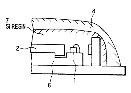
A mounting structure filled with resin in the preferred
embodiment according to the invention will be explained in FIGS.3A
and 3B. FIG.3A is a perspective view showing the mounting structure
and FIG.3B is a partial cross sectional view cut along the line X-X'
in FIG.3A.
Referring to FIGS.3A and 3B, the surface of resin 7 with which
the optical coupling system is covered is further covered with resin
8 for blocking the permeation of moisture. Thus, it can bring an
airtight sealing effect for the optical coupling system. Therefore,
a package and a cap used in the conventional airtight sealing are
not needed.
Next, theabove-mentioned embodimentswillbe further explained
with reference to specific examples thereof. As described above,
FIGS.2A and2B show the high-efficiency optical coupling systemusing
the gel silicon resin 7. In order to give the optimum coupling when
the LD element 1 and the optical fiber 2 are mounted without any
regulation, a marker for the mounting of the LD element 1 is formed
on the silicon substrate by patterning, and the V-groove 5 for the
guiding of the fiber is formed by silicon anisotropic etching.
On the silicon substrate 6, the normal optical fiber 2 or the
ball-tipped fiber 10 which has, as shown in FIG.2B, a hemispherical
tip portion formed by etching etc. and the ~D element 1 are mounted
without any regulation. Then, the clearance between the LD element
1 and the optical fiber 2 or 10 is filled with liquid silicon resin
7.
After filling with silicon resin 7, it is solidified into gel
state by ultraviolet radiation or heating to finish the optical
CA 02229~70 l998-02-l2
coupling system.
In general, when the lens 3 or ball-tipped fiber 10 is used,
the tolerance in the optimum coupling of the LD element 1 and optical
fiber 2 becomes less than 1 ~m. Namely, the high-precision mounting
of both the LD element 1 and optical fiber 2 is required. In case
of the optical coupling system where gel silicon resin 7 is used,
the refractive index of gel silicon resin 7 lies between that of the
air and that of the optical fiber. Therefore, the spot size of beams
emitted from the LD element 1 can be enlarged, thereby increasing
o the coupling tolerance to the optical fiber. Thus, the optical
coupling system in this embodiment, which has the simple composition
employing resin, can realize the high-efficiency coupling of the LD
element and the optical fiber 2 without any regulation.
FIGS.3A and 3B show an example where gel silicon rein 7 and
moisture-blocking resin 8 are used for the airtight sealing of the
optical system. The coupling of the LD element 1 and the optical
fiber 2 is, as described earlier, easily conducted on the silicon
substrate6withoutany regulationbyusinggel siliconresin7. Then,
the surface of gel silicon resin 7 with which the optical coupling
system is covered is further covered with resin 8 for blocking the
permeation of moisture.
In this embodiment, which employs the structure to be covered
with two kinds of resins, the conventional airtight sealing structure
needed for optical modules is not necessary.
By using gel resin with a refractive index higher than that of
the air and lower than that of the optical fiber for the coupling
system of the LD element and the ball-tipped optical fiber, the
coupling tolerance(2 dB down) is relaxed to be greater than 20
CA 02229~70 l998-02-l2
~m in the optical axis direction as shown in FIG.5A and to be greater
than 1.5 ~m in the perpendicular direction of optical axis as shown
in FIG.5B. Therefore, the high-efficiency optical coupling system
using the silicon substrate 6 can be realized without any regulation.
Meanwhile, FIG.5Ashowsa relationbetween the distance (~m) between
the LD elementandoptical fiberandthe couplingloss (dB), andFIG.5B
shows a relation between the amount of shifting (~m) in the direction
perpendicular to the optical axis and the coupling loss (dB).
In these embodiments, by using gel rein, the filling process
o into the optical system can be facilitated and the workability can
be improved as compared the filling process of liquid in the
conventional optical coupling system. Furthermore, since gel resin
has a high elasticity, it can be filled without applying any stress
to the optical fiber or IC wiring.
A mountingstructureofanopticalcouplingsystemwithgel resin
onto an interface substrate in the preferred embodiment according
to the invention will be explained in FIGS.4A and 4B. FIG.4A is a
perspective view showing the mounting structure and FIG.4B is a
partial cross sectional view cut along the line X-X' in FIG.3A.
Referring to FIG.4A, on an interface substrate 11 where LSI 9
for driving the LD element etc. is mounted, the optical coupling
system using gel silicon resin 7 as explained in the aboveembodiments
is directly mounted. Then, the optical coupling system and LSI 9
are covered with the moisture-blocking resin 8.
In this embodiment, which employs such a mounting structure,
the conventional processes that the optical coupling system is
mounted in a package, airtight-sealed and then mounted on the
interface substrate 11 are not necessary. Thus, the interface
CA 02229~70 1998-02-12
- 10-
substrate 11 can be easily fabricated.
When conductive resin is used as the moisture-blocking resin
8, the shield effect for LSI 9 can be also obtained thereby.
Although the invention has been described with respect to
specific embodiment for complete and clear disclosure, the appended
claims are not to be thus limited but are to be construed as embodying
all modification and alternative constructions that may be occurred
to one skilled in the art which fairly fall within the basic teaching
o here is set forth.