Note: Descriptions are shown in the official language in which they were submitted.
CA 02229684 1998-02-16
Device for Identifying the Switched Position
in Electrical Switch Gear
The present imiention relates to a device for identifying the switched
position of electrical
switch gear, in which the position and/or the movement status of a movable
switch contact is
identified by the interaction of a reflecting element that is connected with
the moving part of
the switch geai- with a beam of light.
A device of this type is described, for example, in patent specification DD
133 872. In this
known device, screens or mirrors are arranged in a high voltage switching
apparatus at high-
voltage potential, and these screens or mirrors pass, block, or reflect a beam
of light that is
introduced into the device according to the position of the switch gear.
To this end, screens or mirrors are used, and these are secured to the parts
of the high-voltage
switch gear that are moved..
Major technical difficulties are encountered when securing elements such as
screens, filters,
mirrors, and the like to the parts of the switch gear that are moved. On the
one hand, the
attachment must be able to withstand very high mechanical loads since the
components of the
switch are exposed to major accelerating forces during the switching process;
on the other
hand, chemically harsh environmental conditions prevail, in particular, in
encapsulated switch
gear that is that is filled with an insulating gas. For the remainder, once
they have been
installed, such elements have to be calibrated or the positioning of the
elements has to be
checked.
]
CA 02229684 2007-04-19
20365-3806
For this reason, it is the task of the present
invention to configure appropriate reflective elements in a
way that is simple from the design standpoint, and also to
simplify assembly and initial operation.
This problem has been solved by the present
invention in that the reflective element comprises at least
one reflective surface that is formed by stamping the
surface of a metallic component of the switch gear.
In accordance with one aspect of the present
invention, there is provided a device for identifying the
switched position of electrical switching gear in which the
position of a moving contact is identified by the
interaction of a reflective element that is connected with
the kinematic chain of the switch gear with a beam of light,
wherein the beam is reflected by the reflective element in a
defined position of the moving contact and the reflective
element is formed by at least one reflective surface that is
produced by stamping the surface of a metallic component of
the switch gear.
In accordance with another aspect of the present
invention, there is provided a procedure for manufacturing a
device as defined in the previous aspect, comprising
stamping the surface of the metallic component with a die to
produce the reflective surface and silvering the surface of
the metallic component before it is stamped.
When this method according to the present
invention is used, there is no need for any additional parts
that have to be structurally connected to the elements of
the switch gear. On the one hand, this reduces manufacturing
costs and, on the other hand, it reduces the costs incurred
for putting the device into operation. The stamping can be
2
CA 02229684 2007-04-19
20365-3806
carried out in such a manner that no additional adjustment
is required once the switch gear has been assembled. There
is no danger of any loss of adjustment after the switch gear
has been in use for a protracted period, so that the present
invention assures simple, cost effective switch-position
identification in a switch gear that remains reliable over
the long term.
One advantageous version of the present invention
provides for the fact that the reflective element comprises
a combination of at least two reflective surfaces that are
arranged so as to be at an approximate right angle to each
other.
Configuration in the form of two reflective
surfaces that are arranged at right angles to each other
ensures that an incident beam of light will be reflected
back parallel to the incident direction (triple-mirror
reflection principle). The reflective element can be in the
form of a
2a
CA 02229684 1998-02-16
saw-tooth structure with reflective surfaces that are at right angles to each
other. In such a
case, a reflective surface plane that is perpendicular to the two planes of
the reflective surfaces
referred to above can be dispensed with if the beam of light is fanned out
widely enough in this
direction, or if there is an appropriate tolerance in this direction during
detection of the beam
of reflected light.
It is particularly advantageous that the reflecting element is arranged on a
contact that is
moved during the switching process.
In this case, direct identification of the switch position takes place at the
contact itself, i.e., at
the end of the kinematic train between the switch drive and the driven
contact. Thus, no
transmission errors can occur when the switch position is indicated because of
the fact that the
kinematic train is interrupted ahead of the actual contact.
A further advantageous version of the present intention is such that the
reflective surface(s)
is/are arranged in an area of the moving contact, across which the contact
fingers of a
matching context slide during the switching process; and such that the
reflective surface(s)
is/are configured to be narrower transversely to the direction of movement of
the contact than
the associated surface of the contact fingers.
This configuration ensures that the reflective surface is not damaged by the
contact fingers of
the opposite contact sliding across it during the switching process.
3
CA 02229684 1998-02-16
In order to achieve a high degree of reflectivity for the reflective element,
it has been found to
be advantageous that the reflective surface be silvered.
In addition to this, it can also be an advantage if the present invention be
in the form of switch
gear that has a metallic encapsulating housing with at least one window, it
being possible to
direct the beam of light through the window and into the encapsulating housing
from the
outside, there being a photosensitive element to identify the beam of light
that is reflected by
the reflective elements installed outside said encapsulating housing.
Generation of the beam of light and identification of the beam of light that
is reflected are thus
effected at ground potential, outside a specially grounded metal capsule,
whereas the reflective
element itself is at high-voltage potential. Adjustment of the beam of light
can thus be effected
without any danger, at ground potential, and the voltage supply of an
appropriate light-
emitting element, which would be difficult at high-voltage potential, can be
managed very
simply.
The present invention also relates to a procedure for manufacturing a device
according to the
present invention, in which a reflective surface is generated in one contact
of the switch gear
by stamping the surface with a die. 20
It is also advantageous that the surface be silvered before it is stamped.
The present invention will be described in greater detail below on the basis
of the drawings
appended hereto. These drawings show the following:
4
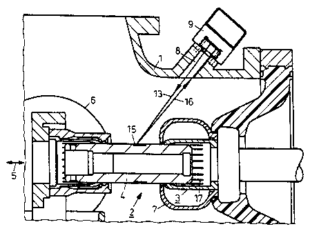
CA 02229684 1998-02-16
Figure 1: a diagrammatic cross section of part of a high-voltage switch;
Figure 2 an erilarged diagrammatic view of the reflective element and a
stamping die in a
longitudinal cross section of the cylindrical contact pin.
An isolating switch 2 is arranged within a metallic encapsulating housing 1,
where it is
surrounded by sulphur hexafluoride as an insulating gas; this isolating switch
2 incorporates a
fixed, bell-shaped contact 3 as a fixed contact with spring contact fingers
17, and a moving
contact in the form of a hollow contact pin 4. The contact pin 4 is moved, in
a manner not
described in greater detail herein, in the direction indicated by the arrow 5
by a drive system
(not shown herein) in order to move it between a power-on and a power-off
position. The
drawing also shows screening electrodes 6, 7.
The encapsulating housing I incorporates a window 8 on which is mounted a
device 9 for
emitting and receiving or identifying beams of light; this is in the form of a
laser or a laser
diode, for example, and a photo sensitive semiconductor element.
Thus, light can be radiated into the encapsulating housing 1 through the
window 8 in the
direction of the moving contact pin 4.
The surface ofthe contact pin 4 is stamped, as is shown in greater detail in
Figure 2. The
stamping 1 is in the form of saw-tooth reflective surfaces 10, 11, and 12 and
each pair of said
surfaces is arranged so as to be essentially perpendicular to each other and
so as to subtend an
angle of approximately 45 with the cylindrical axis of the contact pin 4.
The reflective
surfaces 10, 11, and 12 are flat and sufficiently smooth that they will
reflect an incident been
5
CA 02229684 1998-02-16
incident been 13 with a high degree of reflectioii. The arrangement of the
individual reflective
surfaces in the form that is shown entails the advantage that a beam of light
will be reflected
either only on one or on two reflective surfaces 10, 11, and 12, regardless of
the direction
from which the beam is radiated, and will be reflected back in the opposite
direction to the
incident beam inore or less precisely (three-mirror reflection principle).
The reflective surfaces are both silvered and polished.
During the production of the reflective element, which is formed by the
reflective surfaces 10,
11, and 12, first of all the cylindrical outside surface of the contact pin 4
is silvered and
polished. Next, the surface of the contact pin 4 is stamped with an impression
that in
longitudinal section is of a saw-tooth form, this being done by means of a
stamping die 40.
The contact pii14 is best supported on its inside when this stamping process
is carried out.
The high quality of the contact pin surface with respect to the reflection
factor in the optical
range is retained during such a stamping process, since the surface of the
stamping die 14 is
also extremely smooth. The silvering is preserved and remains even and smooth
when this is
done.
In the switch position as shown in Figure 1, the incident beam 13 will be
reflected back by the
reflective element 15 to the sending and receiving unit 9, in the direction
indicated by the
arrow 16, by the device described above. There, the beam of light 16 that has
been reflected
back is recorded , or information to the effect that the contact pin is
located in the power-on
position is passed on to a further processing unit.
6
CA 02229684 1998-02-16
If the position of the contact pin 4 is changed or if, on being switched on,
it does not move
completely into the contact 3, then the sending and receiving unit 9 reports
that the contact pin
is not in the intended position and that the switch is defective.
The device described above thus provides an extremely reliable, maintenance-
free switch
position indicator, and does so in a simple manner.
7