Language selection

Search

Patent 2229817 Summary

Third-party information liability

Some of the information on this Web page has been provided by external sources. The Government of Canada is not responsible for the accuracy, reliability or currency of the information supplied by external sources. Users wishing to rely upon this information should consult directly with the source of the information. Content provided by external sources is not subject to official languages, privacy and accessibility requirements.

Claims and Abstract availability

Any discrepancies in the text and image of the Claims and Abstract are due to differing posting times. Text of the Claims and Abstract are posted:

  • At the time the application is open to public inspection;
  • At the time of issue of the patent (grant).
(12) Patent: (11) CA 2229817
(54) English Title: CONTACT BLOCK HAVING SNAP IN FEATURES
(54) French Title: BLOC DE CONTACT FIXE PAR ENCLIQUETAGE
Status: Expired and beyond the Period of Reversal
Bibliographic Data
(51) International Patent Classification (IPC):
  • H01R 09/22 (2006.01)
  • H01R 04/58 (2006.01)
  • H01R 13/22 (2006.01)
(72) Inventors :
  • RUTH, BARBARA A. (United States of America)
  • CLARK, AARON P. (United States of America)
  • AUSTIN, MICHEAL M. (United States of America)
  • KLEINERT, RAYMOND J. (United States of America)
(73) Owners :
  • MOTOROLA, INC.
(71) Applicants :
  • MOTOROLA, INC. (United States of America)
(74) Agent: GOWLING WLG (CANADA) LLP
(74) Associate agent:
(45) Issued: 2001-01-02
(86) PCT Filing Date: 1996-08-20
(87) Open to Public Inspection: 1997-03-06
Examination requested: 1998-02-18
Availability of licence: N/A
Dedicated to the Public: N/A
(25) Language of filing: English

Patent Cooperation Treaty (PCT): Yes
(86) PCT Filing Number: PCT/US1996/013442
(87) International Publication Number: US1996013442
(85) National Entry: 1998-02-18

(30) Application Priority Data:
Application No. Country/Territory Date
08/520,359 (United States of America) 1995-08-28

Abstracts

English Abstract


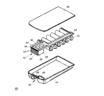
A contact block (10) is provided with a first ledge (34) and a second ledge
(38) that deflectably engage a first edge (46) and a second edge (48) of an
opening (44) in the housing (42) of an electrical device. The contact block
(10) mechanically supports at least one electrical contact (14) to provide a
contact surface (18) whereby the first electrical device (40) may be
electrically interconnected with a second electrical device (60). The contact
block (10) is snapped into place during assembly until it is secured during a
final assembly operation.


French Abstract

Bloc de contact (10) comportant un premier rebord (34) et un second rebord (38) qui sont fixés, de manière à pouvoir être défléchis, à un premier bord (46) et à un second bord (48) d'une ouverture (44) pratiquée dans le boîtier (42) d'un dispositif électrique. Le bloc de contact (10) porte mécaniquement un ou plusieurs contacts électriques (14) de façon à constituer une surface de contact (18), le premier dispositif électrique (40) pouvant être électriquement relié à un second dispositif électrique (60). Le bloc (10) est mis en place par encliquetage durant le montage jusqu'à l'opération de montage final, au cours de laquelle il est fixé.

Claims

Note: Claims are shown in the official language in which they were submitted.


Claims
1. A contact block for electrically interconnecting a first electrical
device with a second electrical device, said first electrical device having an
electrical circuit and a housing, a opening having first and second edges
formed in said housing, said contact block comprising:
a body having a top, bottom, front, back and two opposing sides, said
top defining a first edge along said front, said bottom defining a second
edge along said back, said body fabricated of an electrically insulative
material;
at least one electrical contact disposed in said body of said contact
block, and having a first contact surface for electrically connecting with said
electrical circuit of said first electrical device, and a second contact surfacefor electrically connecting with said second electrical device;
a first ledge formed along at least a portion of said first edge of said
body for deflectably engaging said first edge of said opening in said housing;
and
a second ledge formed along at least a portion of said second edge of
said body for deflectably engaging said second edge of said opening formed
in said housing.
2. A contact block as defined in, claim 1, wherein said at least one
electrical contact further comprises a third surface disposed on said bottom
of said body for electrically interconnecting said first electrical device with a
third electrical device.
3. A contact block as defined in claim 1, wherein said at least one
electrical contact is at least two electrical contacts.
4. A contact block as defined in claim 3, wherein said second
surfaces of said at least two electrical contacts are recessed in said body.
5. A contact block as defined in claim 1, wherein said first ledge
extends along all of said first edge of said body.
6. A contact block as defined in claim 1, wherein said second ledge
extends along all of said second edge of said contact body.

7. A contact block as defined in claim 1, wherein said first contact
surface of said at least one electrical contact is disposed on said top of said
body.
8. A contact block as defined in claim 1, wherein said first contact
surface extends from said back of said body.
9. A contact block as defined in claim 1, wherein said first electrical
device is a battery pack.
10. A contact block as defined in claim 1, wherein said contact block
produces both audible and tactile feed back when asembled into said first
electronic device.

Description

Note: Descriptions are shown in the official language in which they were submitted.


-
CA 02229817 1998-02-18
W O 97/08777 PCT~US96/13442
CONTACT BLOCK HAVING SNAP IN FEATURES
Technical Field
This invention relates in general to connectors for electrical devices,
and more particularly to contact blocks for supporting electrical contacts
used for electrically interconnecting electrical devices.
Background
Electronic and electrical devices are being made for an increasing
number of applications. Cellular phones, palm top computers, scanners,
power tools, and digital cameras are but a few examples. Many of these
devices must electrically interconnect with another device, typically at least
a battery pack and a battery charger. The electrical connections required to
successfully mate two devices must be mechanically supported to ensure
sufficient pressure between the device connectors.
There are a large number of connector styles currently being
marketed. These can all be lumped into one of three categories: pin, card
edge, and surface. The pin type connectors comprise variations of the
male-female type connector in which a pin shaped conductor offered by a
first device is received in a corresponding socket of a second device. The
card edge type connectors are typically found in computer systems
applications where a sub-system board is added to a larger system.
~onductor traces or runners are deposited on circuit boards at the edge of
the board and are connected to the circuit of the board. These edges are
received in a corresponding socket when the board is installed. Surface
type connectors rely on pressing two generally flat conductor surfaces
together to make the connection. This type is the most versatile and has a
wide variety of embodiments.
Of the three, the surface type is most suited for rugged applications.
Pin type connectors work well in applications where the equipment is
generally stationary during operation, such as power cords or computer
cables. If they experience rough treatment it's likely that the pins will
shear off, and disable the equipment. Edge type connectors are intended for
an even more lasting connection. Once a board is installed it is typically a
period of months, and likely years before it is removed. These type of
connectors do not bear repeated installation and removal because it wears
down the conductor on the board edge. Surface type connectors however

CA 02229817 1998-02-18
W O 97/08777 PCT~US96/13442
offer a durable and rugged alternative. Many systems take advantage of
this type of connector including, but not limited to, telephone jacks,
automotive connectors, and battery packs.
The typical surface contact is a flat conductor mechanically
supported by an electrically insulative material such as plastic. In many
applications there are numerous electrical connections that need to be
made between two electrical devices, and care must be taken to ensure
proper alignment. One common way of providing alignment of contacts
between two devices is to employ a connector or contact block. The
10 contacts are embedded in a block of, for example, plastic, leaving the
contact surface exposed on a portion of the block.
However, while the contact block approach has solved the problem
of alignment between adjacent contacts, problems during assembly have
come to light. A significant drawback to the contact block approach is the
15 time needed for assembly of a device incorporating one. Care must be
taken to insure that the block stays in place while the various device
component are assembled until the block can be secured. Therefore there
exists a need to provide a contact block with a means to secure it's position
during assembly until the block can be secured in place.
Brief Description of the Drawings
FIG. 1 is a perspectiye view of a contact block in accordance with the
invention;
FIG. 2 is an exploded view of a battery pack in accordance with the
invention;
FIG. 3 is a side cutaway view of a contact block assembled into the
housing of an electrical device in accordance with the invention; and
FIG. 4 is a perspective view of an alternative embodiment of a
contact block in accordance with the invention.
Detailed Description of the Prefelled Embodiment
While the specification concludes with claims defining the features
of the invention that are regarded as novel, it is believed that the t
invention will be better understood from a consideration of the following
3~ description in conjunction with the drawing figures, in which like
reference numerals are carried forward.
Referring now to FIG. 1, where there is illustrated therein a
perspective view of a contact block 10 in accordance with the instant

CA 02229817 1998-02-18
W O 97/08777 PCT~US96/13442
invention. The contact block has a body 12 which is fabricated from an
electrically insulative material such as, for example, plastic. At least one
electrical contact 14 is disposed in the body 12, and has a first contact surface
16 and a second contact surface 18. The electrical contact is fabricated from
an electrically conductive material, and is preferably a metal insert molded
into the body 12. In many cases, at least two electrical contacts will be
required, and when two or more are present, they are preferably recessed
slightly into the body 12 so that ridges 15 separate the electrical contacts.
The purpose of recessing the electrical contacts is to reduce the risk of
1 0 shorting the contacts together, such as by a coin or keys.
In general, the body 12 has six surfaces such as top 20, bottom 22,
front 24, back 26, and two opposing sides 27 and 28. The first contact surface
16 may be located, for example, on top 20, and the second contact surface on
another surface such as front 24. It is contemplated that a third contact
1 5 surface 30 may be used in some cases, and as such, the third contact surface30 could be located on the bottom 22 of the body. In all instances where a
contact surface is located on a surface of the body, the contact surface and
the body surface are generally co-planar.
Where two surfaces come together, an edge is defined. Top 20 and
front 24 define a first edge 32, which has a first ledge 34 formed along the
length of the first edge. It is contemplated that the first ledge need not be
formed along the entire length of the first edge, but should be formed
along at least a portion of the first edge. Similarly, a second edge 36 is
defined where bottom 22 and back 26 rr~eet, and a second ledge 38 is formed
along second edge 36.
To illustrate how contact block 10 functions in an electrical device,
FIG. 2 shows the incorporation of the contact block into a battery pack 40.
Referring now to FIG. 2, there is illustrated therein generally an exploded
view of a battery pack 40. The battery pack comprises housing 42 which is
preferably molded plastic, and is somewhat resilient. An opening 44 is
formed in the housing, and has a first edge 46 and a second edge 48. Both
edges of the opening 44 are chamfered to facilitate assembly, as will be
described below.
Contact block 10 is shown connected to an electrical circuit 50, which
in the case of a battery pack, includes at least one battery cell 52. The circuit
components 54 may be carried on a flexible circuit board 56. In other cases
the circuit board 56 may be a more typical rigid board, but it is preferred thatthe connection between the board and contact block be a flexible carrier, the

CA 02229817 1998-02-18
W O 97/08777 PCT~US96/1344t
carrier being connected to the first contact surface(s) shown in FIG. 1. This
will facilitate assembly.
Upon assembly, the circuit portion comprising contact block 10,
electrical circuit 50, and battery cell(s) 52, is placed into housing 42. The
contact block is snapped into place in opening 44 by engaging the front 24 of
the contact block with the first edge of the opening, and the bottom 22 of
the contact block with second edge of the opening. A small amount of
force applied to the contact block is transmitted to the edges of the opening,
causing them to deflect slightly, until first ledge 34 and second ledge 38
1 0 become engaged with first edge 46 and second edge 48, respectively. This
produces both audible and tactile feed back; a snap can be heard and felt by
someone assembling the device. When assembled, contact surface 18 is
accessible through opening 44. By snapping the contact block into place, it
is held throughout the assembly process. The battery pack 40, or similar
1 5 electrical device, can be manipulated without moving the contact block out
of it's position. In practice this significantly improves assembly time of an
electrical device, such as battery pack 40. Once the circuit portion is in
place, and contact block 10 is engaged, cover 58 is attached to housing 42 by,
for example, ultrasonic welding. The final position of the cover is such
that it locks the contact block in place, and thereby prevents unintentional
disengagement of the contact block from the housing.
FIG 3 shows the final assembly in more detail. Referring now to FIG.
3, where there is illustrated therein a side cutaway view of contact block 10
assembled into housing 42. From this view the engagement of first ledge 34
and second ledge 38 of the contact block with first edge 46 and second edge 48
of the opening of the housing can be seen. The first contact surface 16 is
connected to circuit board or carrier 56, thereby allowing an electrical
interconnection through exposed contact surface 18 with a second electrical
device 60 when moved in the direction of arrow 62. The second electrical
device could be, for example, a charger. In some cases, a third electrical
device 64 may be simultaneously connected by contacting contact surface 66
of the third electrical device with a third contact surface 68 of contact 14 on
the bottom 22 of the contact block 10. The third electrical device could be, forexample, a cellular phone. It is quite common for the exemplary devices
3~ given, i.e. a battery pack, charger, and cellular phone, to be simultaneously
interconnected. It should be appreciated however that the invention may be
practiced in a wide variety of such devices.

CA 02229817 1998-02-18
W O 97/08777 PCTrUS96/13442
FIG. 4 illustrates an alternate preferred embodiment of contact block
10. As shown in FIG. 4, electrical contact 14 is configured such that a tab of
the conducting material extends from the back 26 of the body 12. This leaves
the first contact surface 16 exposed at a position behind the body instead of
5 on the top 20. This provides a location for connecting to a circuit board, as in
FIG. 2. However, the back surface of the body acts as a guide to align the
circuit board during assembly.
While the preferred embodiments of the invention have been
illustrated and described, it will be clear that the invention is not so limited.
10 Numerous modifications, changes, variations, substitutions and equivalents
will occur to those skilled in the art without departing from the spirit and
scope of the present invention as defined by the appended claims.
What is claimed is:

Representative Drawing
A single figure which represents the drawing illustrating the invention.
Administrative Status

2024-08-01:As part of the Next Generation Patents (NGP) transition, the Canadian Patents Database (CPD) now contains a more detailed Event History, which replicates the Event Log of our new back-office solution.

Please note that "Inactive:" events refers to events no longer in use in our new back-office solution.

For a clearer understanding of the status of the application/patent presented on this page, the site Disclaimer , as well as the definitions for Patent , Event History , Maintenance Fee  and Payment History  should be consulted.

Event History

Description Date
Time Limit for Reversal Expired 2006-08-21
Inactive: IPC from MCD 2006-03-12
Letter Sent 2005-08-22
Inactive: Cover page published 2001-01-02
Grant by Issuance 2001-01-02
Pre-grant 2000-09-19
Inactive: Final fee received 2000-09-19
Notice of Allowance is Issued 2000-03-23
Letter Sent 2000-03-23
Inactive: Approved for allowance (AFA) 2000-02-29
Classification Modified 1998-05-22
Inactive: IPC assigned 1998-05-22
Inactive: First IPC assigned 1998-05-22
Inactive: IPC assigned 1998-05-22
Inactive: Acknowledgment of national entry - RFE 1998-05-11
Application Received - PCT 1998-05-07
All Requirements for Examination Determined Compliant 1998-02-18
Request for Examination Requirements Determined Compliant 1998-02-18
Application Published (Open to Public Inspection) 1997-03-06

Abandonment History

There is no abandonment history.

Maintenance Fee

The last payment was received on 2000-06-23

Note : If the full payment has not been received on or before the date indicated, a further fee may be required which may be one of the following

  • the reinstatement fee;
  • the late payment fee; or
  • additional fee to reverse deemed expiry.

Patent fees are adjusted on the 1st of January every year. The amounts above are the current amounts if received by December 31 of the current year.
Please refer to the CIPO Patent Fees web page to see all current fee amounts.

Owners on Record

Note: Records showing the ownership history in alphabetical order.

Current Owners on Record
MOTOROLA, INC.
Past Owners on Record
AARON P. CLARK
BARBARA A. RUTH
MICHEAL M. AUSTIN
RAYMOND J. KLEINERT
Past Owners that do not appear in the "Owners on Record" listing will appear in other documentation within the application.
Documents

To view selected files, please enter reCAPTCHA code :


To view images, click a link in the Document Description column. To download the documents, select one or more checkboxes in the first column and then click the "Download Selected in PDF format (Zip Archive)" or the "Download Selected as Single PDF" button.

List of published and non-published patent-specific documents on the CPD .

If you have any difficulty accessing content, you can call the Client Service Centre at 1-866-997-1936 or send them an e-mail at CIPO Client Service Centre.


Document
Description 
Date
(yyyy-mm-dd) 
Number of pages   Size of Image (KB) 
Abstract 1998-02-17 1 48
Description 1998-02-17 5 271
Claims 1998-02-17 2 63
Drawings 1998-02-17 4 55
Representative drawing 1998-05-26 1 6
Representative drawing 2000-12-05 1 10
Reminder of maintenance fee due 1998-05-10 1 111
Notice of National Entry 1998-05-10 1 202
Courtesy - Certificate of registration (related document(s)) 1998-05-10 1 117
Commissioner's Notice - Application Found Allowable 2000-03-22 1 164
Maintenance Fee Notice 2005-10-16 1 173
PCT 1998-02-17 6 236
Correspondence 2000-09-18 1 31