Sélection de la langue

Search

Sommaire du brevet 2229817 

Énoncé de désistement de responsabilité concernant l'information provenant de tiers

Une partie des informations de ce site Web a été fournie par des sources externes. Le gouvernement du Canada n'assume aucune responsabilité concernant la précision, l'actualité ou la fiabilité des informations fournies par les sources externes. Les utilisateurs qui désirent employer cette information devraient consulter directement la source des informations. Le contenu fourni par les sources externes n'est pas assujetti aux exigences sur les langues officielles, la protection des renseignements personnels et l'accessibilité.

Disponibilité de l'Abrégé et des Revendications

L'apparition de différences dans le texte et l'image des Revendications et de l'Abrégé dépend du moment auquel le document est publié. Les textes des Revendications et de l'Abrégé sont affichés :

  • lorsque la demande peut être examinée par le public;
  • lorsque le brevet est émis (délivrance).
(12) Brevet: (11) CA 2229817
(54) Titre français: BLOC DE CONTACT FIXE PAR ENCLIQUETAGE
(54) Titre anglais: CONTACT BLOCK HAVING SNAP IN FEATURES
Statut: Périmé et au-delà du délai pour l’annulation
Données bibliographiques
(51) Classification internationale des brevets (CIB):
  • H01R 09/22 (2006.01)
  • H01R 04/58 (2006.01)
  • H01R 13/22 (2006.01)
(72) Inventeurs :
  • RUTH, BARBARA A. (Etats-Unis d'Amérique)
  • CLARK, AARON P. (Etats-Unis d'Amérique)
  • AUSTIN, MICHEAL M. (Etats-Unis d'Amérique)
  • KLEINERT, RAYMOND J. (Etats-Unis d'Amérique)
(73) Titulaires :
  • MOTOROLA, INC.
(71) Demandeurs :
  • MOTOROLA, INC. (Etats-Unis d'Amérique)
(74) Agent: GOWLING WLG (CANADA) LLP
(74) Co-agent:
(45) Délivré: 2001-01-02
(86) Date de dépôt PCT: 1996-08-20
(87) Mise à la disponibilité du public: 1997-03-06
Requête d'examen: 1998-02-18
Licence disponible: S.O.
Cédé au domaine public: S.O.
(25) Langue des documents déposés: Anglais

Traité de coopération en matière de brevets (PCT): Oui
(86) Numéro de la demande PCT: PCT/US1996/013442
(87) Numéro de publication internationale PCT: US1996013442
(85) Entrée nationale: 1998-02-18

(30) Données de priorité de la demande:
Numéro de la demande Pays / territoire Date
08/520,359 (Etats-Unis d'Amérique) 1995-08-28

Abrégés

Abrégé français

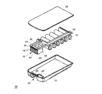
Bloc de contact (10) comportant un premier rebord (34) et un second rebord (38) qui sont fixés, de manière à pouvoir être défléchis, à un premier bord (46) et à un second bord (48) d'une ouverture (44) pratiquée dans le boîtier (42) d'un dispositif électrique. Le bloc de contact (10) porte mécaniquement un ou plusieurs contacts électriques (14) de façon à constituer une surface de contact (18), le premier dispositif électrique (40) pouvant être électriquement relié à un second dispositif électrique (60). Le bloc (10) est mis en place par encliquetage durant le montage jusqu'à l'opération de montage final, au cours de laquelle il est fixé.


Abrégé anglais


A contact block (10) is provided with a first ledge (34) and a second ledge
(38) that deflectably engage a first edge (46) and a second edge (48) of an
opening (44) in the housing (42) of an electrical device. The contact block
(10) mechanically supports at least one electrical contact (14) to provide a
contact surface (18) whereby the first electrical device (40) may be
electrically interconnected with a second electrical device (60). The contact
block (10) is snapped into place during assembly until it is secured during a
final assembly operation.

Revendications

Note : Les revendications sont présentées dans la langue officielle dans laquelle elles ont été soumises.


Claims
1. A contact block for electrically interconnecting a first electrical
device with a second electrical device, said first electrical device having an
electrical circuit and a housing, a opening having first and second edges
formed in said housing, said contact block comprising:
a body having a top, bottom, front, back and two opposing sides, said
top defining a first edge along said front, said bottom defining a second
edge along said back, said body fabricated of an electrically insulative
material;
at least one electrical contact disposed in said body of said contact
block, and having a first contact surface for electrically connecting with said
electrical circuit of said first electrical device, and a second contact surfacefor electrically connecting with said second electrical device;
a first ledge formed along at least a portion of said first edge of said
body for deflectably engaging said first edge of said opening in said housing;
and
a second ledge formed along at least a portion of said second edge of
said body for deflectably engaging said second edge of said opening formed
in said housing.
2. A contact block as defined in, claim 1, wherein said at least one
electrical contact further comprises a third surface disposed on said bottom
of said body for electrically interconnecting said first electrical device with a
third electrical device.
3. A contact block as defined in claim 1, wherein said at least one
electrical contact is at least two electrical contacts.
4. A contact block as defined in claim 3, wherein said second
surfaces of said at least two electrical contacts are recessed in said body.
5. A contact block as defined in claim 1, wherein said first ledge
extends along all of said first edge of said body.
6. A contact block as defined in claim 1, wherein said second ledge
extends along all of said second edge of said contact body.

7. A contact block as defined in claim 1, wherein said first contact
surface of said at least one electrical contact is disposed on said top of said
body.
8. A contact block as defined in claim 1, wherein said first contact
surface extends from said back of said body.
9. A contact block as defined in claim 1, wherein said first electrical
device is a battery pack.
10. A contact block as defined in claim 1, wherein said contact block
produces both audible and tactile feed back when asembled into said first
electronic device.

Description

Note : Les descriptions sont présentées dans la langue officielle dans laquelle elles ont été soumises.


-
CA 02229817 1998-02-18
W O 97/08777 PCT~US96/13442
CONTACT BLOCK HAVING SNAP IN FEATURES
Technical Field
This invention relates in general to connectors for electrical devices,
and more particularly to contact blocks for supporting electrical contacts
used for electrically interconnecting electrical devices.
Background
Electronic and electrical devices are being made for an increasing
number of applications. Cellular phones, palm top computers, scanners,
power tools, and digital cameras are but a few examples. Many of these
devices must electrically interconnect with another device, typically at least
a battery pack and a battery charger. The electrical connections required to
successfully mate two devices must be mechanically supported to ensure
sufficient pressure between the device connectors.
There are a large number of connector styles currently being
marketed. These can all be lumped into one of three categories: pin, card
edge, and surface. The pin type connectors comprise variations of the
male-female type connector in which a pin shaped conductor offered by a
first device is received in a corresponding socket of a second device. The
card edge type connectors are typically found in computer systems
applications where a sub-system board is added to a larger system.
~onductor traces or runners are deposited on circuit boards at the edge of
the board and are connected to the circuit of the board. These edges are
received in a corresponding socket when the board is installed. Surface
type connectors rely on pressing two generally flat conductor surfaces
together to make the connection. This type is the most versatile and has a
wide variety of embodiments.
Of the three, the surface type is most suited for rugged applications.
Pin type connectors work well in applications where the equipment is
generally stationary during operation, such as power cords or computer
cables. If they experience rough treatment it's likely that the pins will
shear off, and disable the equipment. Edge type connectors are intended for
an even more lasting connection. Once a board is installed it is typically a
period of months, and likely years before it is removed. These type of
connectors do not bear repeated installation and removal because it wears
down the conductor on the board edge. Surface type connectors however

CA 02229817 1998-02-18
W O 97/08777 PCT~US96/13442
offer a durable and rugged alternative. Many systems take advantage of
this type of connector including, but not limited to, telephone jacks,
automotive connectors, and battery packs.
The typical surface contact is a flat conductor mechanically
supported by an electrically insulative material such as plastic. In many
applications there are numerous electrical connections that need to be
made between two electrical devices, and care must be taken to ensure
proper alignment. One common way of providing alignment of contacts
between two devices is to employ a connector or contact block. The
10 contacts are embedded in a block of, for example, plastic, leaving the
contact surface exposed on a portion of the block.
However, while the contact block approach has solved the problem
of alignment between adjacent contacts, problems during assembly have
come to light. A significant drawback to the contact block approach is the
15 time needed for assembly of a device incorporating one. Care must be
taken to insure that the block stays in place while the various device
component are assembled until the block can be secured. Therefore there
exists a need to provide a contact block with a means to secure it's position
during assembly until the block can be secured in place.
Brief Description of the Drawings
FIG. 1 is a perspectiye view of a contact block in accordance with the
invention;
FIG. 2 is an exploded view of a battery pack in accordance with the
invention;
FIG. 3 is a side cutaway view of a contact block assembled into the
housing of an electrical device in accordance with the invention; and
FIG. 4 is a perspective view of an alternative embodiment of a
contact block in accordance with the invention.
Detailed Description of the Prefelled Embodiment
While the specification concludes with claims defining the features
of the invention that are regarded as novel, it is believed that the t
invention will be better understood from a consideration of the following
3~ description in conjunction with the drawing figures, in which like
reference numerals are carried forward.
Referring now to FIG. 1, where there is illustrated therein a
perspective view of a contact block 10 in accordance with the instant

CA 02229817 1998-02-18
W O 97/08777 PCT~US96/13442
invention. The contact block has a body 12 which is fabricated from an
electrically insulative material such as, for example, plastic. At least one
electrical contact 14 is disposed in the body 12, and has a first contact surface
16 and a second contact surface 18. The electrical contact is fabricated from
an electrically conductive material, and is preferably a metal insert molded
into the body 12. In many cases, at least two electrical contacts will be
required, and when two or more are present, they are preferably recessed
slightly into the body 12 so that ridges 15 separate the electrical contacts.
The purpose of recessing the electrical contacts is to reduce the risk of
1 0 shorting the contacts together, such as by a coin or keys.
In general, the body 12 has six surfaces such as top 20, bottom 22,
front 24, back 26, and two opposing sides 27 and 28. The first contact surface
16 may be located, for example, on top 20, and the second contact surface on
another surface such as front 24. It is contemplated that a third contact
1 5 surface 30 may be used in some cases, and as such, the third contact surface30 could be located on the bottom 22 of the body. In all instances where a
contact surface is located on a surface of the body, the contact surface and
the body surface are generally co-planar.
Where two surfaces come together, an edge is defined. Top 20 and
front 24 define a first edge 32, which has a first ledge 34 formed along the
length of the first edge. It is contemplated that the first ledge need not be
formed along the entire length of the first edge, but should be formed
along at least a portion of the first edge. Similarly, a second edge 36 is
defined where bottom 22 and back 26 rr~eet, and a second ledge 38 is formed
along second edge 36.
To illustrate how contact block 10 functions in an electrical device,
FIG. 2 shows the incorporation of the contact block into a battery pack 40.
Referring now to FIG. 2, there is illustrated therein generally an exploded
view of a battery pack 40. The battery pack comprises housing 42 which is
preferably molded plastic, and is somewhat resilient. An opening 44 is
formed in the housing, and has a first edge 46 and a second edge 48. Both
edges of the opening 44 are chamfered to facilitate assembly, as will be
described below.
Contact block 10 is shown connected to an electrical circuit 50, which
in the case of a battery pack, includes at least one battery cell 52. The circuit
components 54 may be carried on a flexible circuit board 56. In other cases
the circuit board 56 may be a more typical rigid board, but it is preferred thatthe connection between the board and contact block be a flexible carrier, the

CA 02229817 1998-02-18
W O 97/08777 PCT~US96/1344t
carrier being connected to the first contact surface(s) shown in FIG. 1. This
will facilitate assembly.
Upon assembly, the circuit portion comprising contact block 10,
electrical circuit 50, and battery cell(s) 52, is placed into housing 42. The
contact block is snapped into place in opening 44 by engaging the front 24 of
the contact block with the first edge of the opening, and the bottom 22 of
the contact block with second edge of the opening. A small amount of
force applied to the contact block is transmitted to the edges of the opening,
causing them to deflect slightly, until first ledge 34 and second ledge 38
1 0 become engaged with first edge 46 and second edge 48, respectively. This
produces both audible and tactile feed back; a snap can be heard and felt by
someone assembling the device. When assembled, contact surface 18 is
accessible through opening 44. By snapping the contact block into place, it
is held throughout the assembly process. The battery pack 40, or similar
1 5 electrical device, can be manipulated without moving the contact block out
of it's position. In practice this significantly improves assembly time of an
electrical device, such as battery pack 40. Once the circuit portion is in
place, and contact block 10 is engaged, cover 58 is attached to housing 42 by,
for example, ultrasonic welding. The final position of the cover is such
that it locks the contact block in place, and thereby prevents unintentional
disengagement of the contact block from the housing.
FIG 3 shows the final assembly in more detail. Referring now to FIG.
3, where there is illustrated therein a side cutaway view of contact block 10
assembled into housing 42. From this view the engagement of first ledge 34
and second ledge 38 of the contact block with first edge 46 and second edge 48
of the opening of the housing can be seen. The first contact surface 16 is
connected to circuit board or carrier 56, thereby allowing an electrical
interconnection through exposed contact surface 18 with a second electrical
device 60 when moved in the direction of arrow 62. The second electrical
device could be, for example, a charger. In some cases, a third electrical
device 64 may be simultaneously connected by contacting contact surface 66
of the third electrical device with a third contact surface 68 of contact 14 on
the bottom 22 of the contact block 10. The third electrical device could be, forexample, a cellular phone. It is quite common for the exemplary devices
3~ given, i.e. a battery pack, charger, and cellular phone, to be simultaneously
interconnected. It should be appreciated however that the invention may be
practiced in a wide variety of such devices.

CA 02229817 1998-02-18
W O 97/08777 PCTrUS96/13442
FIG. 4 illustrates an alternate preferred embodiment of contact block
10. As shown in FIG. 4, electrical contact 14 is configured such that a tab of
the conducting material extends from the back 26 of the body 12. This leaves
the first contact surface 16 exposed at a position behind the body instead of
5 on the top 20. This provides a location for connecting to a circuit board, as in
FIG. 2. However, the back surface of the body acts as a guide to align the
circuit board during assembly.
While the preferred embodiments of the invention have been
illustrated and described, it will be clear that the invention is not so limited.
10 Numerous modifications, changes, variations, substitutions and equivalents
will occur to those skilled in the art without departing from the spirit and
scope of the present invention as defined by the appended claims.
What is claimed is:

Dessin représentatif
Une figure unique qui représente un dessin illustrant l'invention.
États administratifs

2024-08-01 : Dans le cadre de la transition vers les Brevets de nouvelle génération (BNG), la base de données sur les brevets canadiens (BDBC) contient désormais un Historique d'événement plus détaillé, qui reproduit le Journal des événements de notre nouvelle solution interne.

Veuillez noter que les événements débutant par « Inactive : » se réfèrent à des événements qui ne sont plus utilisés dans notre nouvelle solution interne.

Pour une meilleure compréhension de l'état de la demande ou brevet qui figure sur cette page, la rubrique Mise en garde , et les descriptions de Brevet , Historique d'événement , Taxes périodiques et Historique des paiements devraient être consultées.

Historique d'événement

Description Date
Le délai pour l'annulation est expiré 2006-08-21
Inactive : CIB de MCD 2006-03-12
Lettre envoyée 2005-08-22
Inactive : Page couverture publiée 2001-01-02
Accordé par délivrance 2001-01-02
Préoctroi 2000-09-19
Inactive : Taxe finale reçue 2000-09-19
Un avis d'acceptation est envoyé 2000-03-23
Lettre envoyée 2000-03-23
Inactive : Approuvée aux fins d'acceptation (AFA) 2000-02-29
Symbole de classement modifié 1998-05-22
Inactive : CIB attribuée 1998-05-22
Inactive : CIB en 1re position 1998-05-22
Inactive : CIB attribuée 1998-05-22
Inactive : Acc. récept. de l'entrée phase nat. - RE 1998-05-11
Demande reçue - PCT 1998-05-07
Toutes les exigences pour l'examen - jugée conforme 1998-02-18
Exigences pour une requête d'examen - jugée conforme 1998-02-18
Demande publiée (accessible au public) 1997-03-06

Historique d'abandonnement

Il n'y a pas d'historique d'abandonnement

Taxes périodiques

Le dernier paiement a été reçu le 2000-06-23

Avis : Si le paiement en totalité n'a pas été reçu au plus tard à la date indiquée, une taxe supplémentaire peut être imposée, soit une des taxes suivantes :

  • taxe de rétablissement ;
  • taxe pour paiement en souffrance ; ou
  • taxe additionnelle pour le renversement d'une péremption réputée.

Les taxes sur les brevets sont ajustées au 1er janvier de chaque année. Les montants ci-dessus sont les montants actuels s'ils sont reçus au plus tard le 31 décembre de l'année en cours.
Veuillez vous référer à la page web des taxes sur les brevets de l'OPIC pour voir tous les montants actuels des taxes.

Historique des taxes

Type de taxes Anniversaire Échéance Date payée
Enregistrement d'un document 1998-02-18
Requête d'examen - générale 1998-02-18
Taxe nationale de base - générale 1998-02-18
TM (demande, 2e anniv.) - générale 02 1998-08-20 1998-06-30
TM (demande, 3e anniv.) - générale 03 1999-08-20 1999-07-06
TM (demande, 4e anniv.) - générale 04 2000-08-21 2000-06-23
Taxe finale - générale 2000-09-19
TM (brevet, 5e anniv.) - générale 2001-08-20 2001-06-29
TM (brevet, 6e anniv.) - générale 2002-08-20 2002-06-26
TM (brevet, 7e anniv.) - générale 2003-08-20 2003-07-04
TM (brevet, 8e anniv.) - générale 2004-08-20 2004-07-07
Titulaires au dossier

Les titulaires actuels et antérieures au dossier sont affichés en ordre alphabétique.

Titulaires actuels au dossier
MOTOROLA, INC.
Titulaires antérieures au dossier
AARON P. CLARK
BARBARA A. RUTH
MICHEAL M. AUSTIN
RAYMOND J. KLEINERT
Les propriétaires antérieurs qui ne figurent pas dans la liste des « Propriétaires au dossier » apparaîtront dans d'autres documents au dossier.
Documents

Pour visionner les fichiers sélectionnés, entrer le code reCAPTCHA :


Pour visualiser une image, cliquer sur un lien dans la colonne description du document. Pour télécharger l'image (les images), cliquer l'une ou plusieurs cases à cocher dans la première colonne et ensuite cliquer sur le bouton "Télécharger sélection en format PDF (archive Zip)" ou le bouton "Télécharger sélection (en un fichier PDF fusionné)".

Liste des documents de brevet publiés et non publiés sur la BDBC .

Si vous avez des difficultés à accéder au contenu, veuillez communiquer avec le Centre de services à la clientèle au 1-866-997-1936, ou envoyer un courriel au Centre de service à la clientèle de l'OPIC.


Description du
Document 
Date
(aaaa-mm-jj) 
Nombre de pages   Taille de l'image (Ko) 
Abrégé 1998-02-17 1 48
Description 1998-02-17 5 271
Revendications 1998-02-17 2 63
Dessins 1998-02-17 4 55
Dessin représentatif 1998-05-26 1 6
Dessin représentatif 2000-12-05 1 10
Rappel de taxe de maintien due 1998-05-10 1 111
Avis d'entree dans la phase nationale 1998-05-10 1 202
Courtoisie - Certificat d'enregistrement (document(s) connexe(s)) 1998-05-10 1 117
Avis du commissaire - Demande jugée acceptable 2000-03-22 1 164
Avis concernant la taxe de maintien 2005-10-16 1 173
PCT 1998-02-17 6 236
Correspondance 2000-09-18 1 31