Note: Descriptions are shown in the official language in which they were submitted.
CA 0222997~ 1998-02-18
TITLE OF THE INVENTION
WAFER PROCESSING APPARATUS, WAFER PROCESSING METHOD,
AND SEMICONDUCTOR SUBSTRATE FABRICATION METHOD
BACKGROUND OF THE INVENTION
FIELD OF THE INVENTION
The present invention relates to a wafer processing
apparatus, a wafer processing method, and a
semiconductor substrate fabrication method and, more
particularly, to a wafer processing apparatus for
processing a wafer by dipping it into a processing
solution, a wafer processing method, and a semiconductor
substrate fabrication method.
DESCRIPTION OF THE RELATED ART
Cleaning processing is a typical example of wafer
processing. One subject of wafer cleaning is to increase
the speed. Japanese Patent Laid-Open No. 8-293478 has
disclosed a wafer cleaning method capable of increasing
the cleaning efficiency by supplying ultrasonic waves
while rotating a wafer, and an apparatus for practicing
this method.
The wafer cleaning method disclosed in Japanese
Patent Laid-Open No. 8-293478 is based on the
CA 0222997~ 1998-02-18
recognition that a wafer is most efficiently cleaned at
the interface between a cleaning solution and ambient
atmosphere. In the wafer cleaning method, therefore,
particles inevitably attach to a wafer at the interface
between the cleaning solution and ambient atmosphere.
In the wafer cleaning apparatus disclosed in
Japanese Patent Laid-Open No. 8-293478, a cam mechanism
for rotating a wafer is arranged immediately below the
wafer, so a rotating force is not efficiently
transmitted to the wafer. In the wafer cleaning
apparatus, the transmission of ultrasonic waves is
interrupted because the cam mechanism is laid out to
completely shield the wafer from below. As a result, the
strength of ultrasonic waves differs between the center
and peripheral portion of the wafer, and the wafer
cannot be uniformly processed. This nonuniformity cannot
be improved by rotation of the wafer.
SUMMARY OF THE INVENTION
It is an object of the present invention to prevent
contamination of a wafer by particles in various wafer
processes including cleaning and etching.
It is another object of the present invention to
make wafer processing uniform.
A wafer processing apparatus according to the
CA 0222997~ 1998-02-18
present invention is a wafer processing apparatus for
processing a wafer by dipping the wafer into a
processing solution, characterized by comprising a
processing bath having a depth that~allows to completely
dip the wafer into the processing solution, wafer
rotating means for rotating one or a plurality of wafers
held by a wafer holder by using a wafer rotating member
which rotates about a shaft shifted from a portion
immediately below a barycenter of the one or plurality
of wafers, and ultrasonic generating means for
generating ultrasonic waves in the processing bath.
In the wafer processing apparatus, only the wafer
rotating member is preferably arranged as a member for
transmitting a rotating force to the wafer below the one
or plurality of wafers held by the wafer holder.
In the wafer processing apparatus, the wafer
rotating member preferably comprises at least one rod
member substantially parallel to the shaft, and the rod
member preferably rotates about the shaft.
In the wafer processing apparatus, the rod member
preferably has a diameter much smaller than a diameter
of a cylinder virtually formed upon rotation of the rod
member about the shaft.
In the wafer processing apparatus, the rod member
preferably has a groove which engages with a peripheral
CA 0222997~ 1998-02-18
portion of the wafer.
In the wafer processing apparatus, a section of the
rod member taken along the shaft preferably has a
substantially sine-wave shape.
In the wafer processing apparatus, a section of the
rod member taken along the shaft preferably has a
substantially full-wave rectifying shape.
In the wafer processing apparatus, the wafer
rotating means preferably further comprises driving
force generating means arranged outside the processing
bath, and driving force transmission means for
transmitting a driving force generated by the driving
force generating means to the wafer rotating member and
rotating the wafer rotating member.
The wafer processing apparatus preferably further
comprises a dividing member for dividing an interior of
the processing bath into a processing wafer side and a
side of the driving force transmission means.
In the wafer processing apparatus, the driving
force transmission means preferably transmits the
driving force generated by the driving force generating
means through a crank mechanism.
In the wafer processing apparatus, the processing
bath preferably comprises a circulating mechanism having
an overflow bath.
CA 0222997~ 1998-02-18
In the wafer processing apparatus, the circulating
mechanism preferably comprises contamination reducing
means for reducing contamination of the wafer by
particles.
In the wafer processing apparatus, the
contamination reducing means preferably comprises a
filter.
In the wafer processing apparatus, the
contamination reducing means preferably comprises means
for adjusting flow of the processing solution in the
processing bath.
In the wafer processing apparatus, the ultrasonic
generating means preferably comprises an ultrasonic bath
and an ultrasonic source, and the processing bath
preferably receives ultrasonic waves through an
ultrasonic transmitting medium set in the ultrasonic
bath.
The wafer processing apparatus preferably further
comprises driving means for changing a relative
positional relationship between the ultrasonic source
and a wafer to be processed.
In the wafer processing apparatus, the driving
means preferably moves the ultrasonic source within the
ultrasonic bath.
In the wafer processing apparatus, at least
CA 0222997~ 1998-02-18
portions of constituent members of the processing bath
and the wafer rotating means which may come into contact
with the processing solution are preferably made of one
material selected from the group consisting of quartz
and plastic.
In the wafer processing apparatus, at least
portions of constituent members of the processing bath
and the wafer rotating means which may come into contact
with the processing solution are preferably made of one
material selected from the group consisting of a
fluorine resin, vinyl chloride, polyethylene,
polypropylene, polybutyleneterephthalate (PBT), and
polyetheretherketone (PEEK).
A wafer processing method according to the present
invention is a wafer processing method of processing a
wafer while ultrasonic waves are supplied, characterized
by comprising processing the wafer while entirely
dipping the wafer into a processing solution and
rotating the wafer.
A wafer processing method according to the present
invention is a wafer processing method of processing a
wafer while ultrasonic waves are supplied, characterized
by comprising processing the wafer while entirely
dipping the wafer into a processing solution, and
rotating and vertically moving the wafer.
CA 0222997~ 1998-02-18
A wafer processing method according to the present
invention is a wafer processing method of processing a
wafer while ultrasonic waves are supplied, characterized
by comprising processing the wafer while entirely
dipping the wafer into a processing solution and
changing a position of an ultrasonic source.
The wafer processing method according to the
present invention is characterized in that the wafer is
cleaned using a wafer cleaning solution as the
processing solution.
The wafer processing method is suitable for a
method of etching the wafer using a wafer etching
solution as the processing solution.
The wafer processing method is suitable for a
method of etching a porous silicon layer of a wafer
having the porous silicon layer using a porous silicon
etching solution as the processing solution.
The wafer processing method is suitable for a
method of etching a porous silicon layer of a wafer
having the porous silicon layer using, as the processing
solution, any one of
(a) hydrofluoric acid,
(b) solution mixture prepared by adding at least
one of alcohol and hydrogen peroxide to hydrofluoric
acid,
CA 0222997~ 1998-02-18
(c) buffered hydrofluoric acid,
(d) solution mixture prepared by adding at least
one of alcohol and hydrogen peroxide to buffered
hydrofluoric acid, and
(e) solution mixture of hydrofluoric acid, nitric
acid, and acetic acid.
A semiconductor substrate fabrication method
according to the present invention is characterized by
comprising the step of forming a non porous layer on a
porous layer formed on a surface of a first substrate,
the step of bonding a first substrate side of a
prospective structure and a second substrate prepared
separately to sandwich the non porous layer between the
first substrate side and the second substrate, the
removal step of removing the first substrate from the
bonded structure to expose the porous layer on a second
substrate side thereof, and the etching step of etching
the porous layer while the second substrate side on
which the porous layer is exposed is completely dipped
into an etching solution, and ultrasonic waves are
supplied, thereby exposing surface of the second
substrate side, the etching step rotating the second
substrate side.
A semiconductor substrate fabrication method
according to the present invention is characterized by
- 8 -
CA 0222997~ 1998-02-18
comprising the step of forming a non porous layer on a
porous layer formed on a surface of a first substrate,
the step of bonding a first substrate side of a
prospective structure and a second substrate prepared
separately to sandwich the non porous layer between the
firs-t substrate side and the second substrate, the
removal step of removing the first substrate from the
bonded structure to expose the porous layer on a second
substrate side thereof, and the etching step of etching
the porous layer while the second substrate side on
which the porous layer is exposed is completely dipped
into an etching solution, and ultrasonic waves are
supplied, thereby exposing surface of the second
substrate side, the etching step rotating and vertically
moving the second substrate side.
A semiconductor substrate fabrication method
according to the present invention is characterized by
comprising the step of forming a non porous layer on a
porous layer formed on a surface of a first substrate,
the step of bonding a first substrate side of a
prospective structure and a second substrate prepared
separately to sandwich the non porous layer between the
first substrate side and the second substrate, the
removal step of removing the first substrate from the
bonded structure to expose the porous layer on a second
CA 0222997~ 1998-02-18
substrate side thereof, and the etching step of etching
the porous layer while the second substrate side on
which the porous layer is exposed is completely dipped
into an etching solution, and ultrasonic waves are
supplied, thereby exposing surface of the second
substrate side, the etching step changing a position of
an ultrasonic bath.
The etching solution used in the etching step is
preferably any one of
(a) hydrofluoric acid,
(b) solution mixture prepared by adding at least
one of alcohol and hydrogen peroxide to hydrofluoric
acid,
(c) buffered hydrofluoric acid,
(d) solution mixture prepared by adding at least
one of alcohol and hydrogen peroxide to buffered
hydrofluoric acid, and
(e) solution mixture of hydrofluoric acid, nitric
acid, and acetic acid.
The removal step preferably comprises exposing the
porcus layer by grinding, polishing, or etching the
first substrate from a back surface.
The removal step preferably comprises separating
the first substrate side and the second substrate side
at a boundary of the porous layer.
- 10 -
CA 0222997~ 1998-02-18
The non porous layer is preferably a single-crystal
silicon layer.
The non porous layer is preferably made up of a
sing:le-crystal silicon layer and a silicon oxide layer
formed on the single-crystal silicon layer.
The non porous layer is preferably a compound
semiconductor layer.
The second substrate is preferably a silicon
subs-trate.
The second substrate is preferably a silicon
subs-trate having a silicon oxide film formed on a
surface to be bonded to the first substrate side.
The second substrate is preferably a
light-transmitting substrate.
Further objects, features and advantages of the
present invention will become apparent from the
following detailed description of embodiments of the
present invention with reference to the accompanying
drawings.
BRIEF DESCRIPTION OF THE DRAWINGS
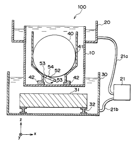
Fig. 1 is a perspective view showing the schematic
construction of a wafer processing apparatus according
to the first embodiment of the present invention;
Fig. 2 is a sectional view of the wafer processing
CA 0222997~ 1998-02-18
apparatus shown in Fig. 1;
Fig. 3 is a perspective view showing an example of
the construction of a wafer rotating member;
Figs. 4A and 4B are views, respectively, showing
the movement of a wafer when the wafer rotating member
is rotated in a lifting direction;
Figs. 5A and 5B are views, respectively, showing
the movement of a wafer having an orientation flat;
Figs. 6A and 6B are sectional views, respectively,
showing another example of the construction of a wafer
rotating rod;
Figs. 7A and 7B are sectional views, respectively,
showing still another example of the construction of the
wafer rotating rod;
Figs. 8A to 8C are views each showing an example of
the shape of the section of the wafer rotating rod;
Fig. 9 is a view showing a mechanism for
transmitting a driving torque generated by a motor to
the rotating shaft of the wafer rotating member; and
Figs. 10A to 10F are views, respectively, showing
the method of fabricating a semiconductor wafer.
DETAILED DESCRIPTION OF THE PREFERRED EMBODIMENTS
Preferred embodiments of the present invention will
be described in detail below with reference to the
CA 0222997~ 1998-02-18
accompanying drawings.
[First Embodiment]
Fig. 1 is a perspective view showing the schematic
construction of a wafer processing apparatus according
to the first embodiment of the present invention. Fig. 2
is a sectional view of the wafer processing apparatus
shown in Fig. 1.
In a wafer processing apparatus 100 according to
this embodiment, portions which may come into contact
with a processing solution are preferably made from
quartz or plastic in accordance with the intended use.
Pref-erable examples of the plastic are a fluorine resin,
vinyl chloride, polyethylene, polypropylene,
polybutyleneterephthalate (PBT), and
polyetheretherketone (PEEK). Preferable examples of the
fluorine resin are PVDF, PFA, and PTFE.
This wafer processing apparatus 100 has a wafer
proc:essing bath 10, an overflow bath 20, an ultrasonic
bath 30, and a wafer rotating mechanism (52 to 59) for
rotating wafers 40.
To process wafers, the wafer processing bath 10 is
filled with a processing solution (e.g., an etching
solution or a cleaning solution). The overflow bath 20
for temporarily storing any processing solution
overflowing from the wafer processing bath 10 is
CA 0222997~ 1998-02-18
provided around the upper portion of the wafer
processing bath 10. The processing solution temporarily
stored in the overflow bath 20 is discharged from the
bott.om portion of the overflow bath 20 to a circulator
21 t.hrough a discharge pipe 21a. The circulator 21
removes particles by filtering the discharged processing
solution and supplies the processing solution to the
bott.om portion of the wafer processing bath 10 through a
supply pipe 21b. Consequently, particles in the wafer
proc:essing bath 10 are efficiently removed.
The wafer processing bath 10 must have a depth by
whic:h the wafers 40 are completely dipped. This prevents
part.icles from attaching to the wafers 40 at the
interface between the processing solution and ambient
atmosphere, and makes processing for the wafers 40
unif~orm.
When wafers are processed by completely dipping
them into the processing solution, and particles attach
to t.he wafers in the processing solution, the particles
easi.ly return into the processing solution. However, if
only parts of wafers are dipped into the processing
solution, particles attaching to the wafers at the
interface between the processing solution and ambient
atmosphere are hardly removed from the wafers, and
exposed to ambient atmosphere while attaching to the
- 14 -
CA 0222997~ 1998-02-18
wafers. Particles thus attaching to wafers are scarcely
removed from the wafers even by dipping the attached
port:ions of the wafers into the processing solution
again. Particularly, when the wafer surface is
hydrophobic (e.g., a silicon wafer not having any
silicon oxide film), particles completely attach to the
wafer surface and become more difficult to remove
because the wafer surface is exposed to a dry atmosphere.
The ultrasonic bath 30 is arranged below the wafer
processing bath 10. An ultrasonic source 31 is supported
by an adjusting mechanism 32 inside the ultrasonic bath
30. This adjusting mechanism 32 includes a mechanism for
adjusting the vertical position of the ultrasonic source
31 and a mechanism for adjusting the horizontal position
of t:he ultrasonic source 31, as mechanisms for adjusting
the relative positional relationship between the
ultrasonic source 31 and the wafer processing bath 10
(waf-ers 90). By this mechanism, ultrasonic waves to be
supplied to the wafer processing bath 10, more
specifically, to the wafers 40 can be optimized. The
ultrasonic source 31 preferably has a function of
adjusting the frequency or strength of ultrasonic waves
to be generated. This further optimizes the supply of
ultrasonic waves.
Since the apparatus thus has the mechanism for
CA 0222997~ 1998-02-18
optimizing the supply of ultrasonic waves to the wafers
40, various types of wafers can be processed. Swinging
the ultrasonic source 31 by the adjusting mechanism 32
while the wafers 40 are processed can make processing
for the wafers 40 uniform. Changing the frequency of
ultrasonic waves while the wafers 40 are processed can
also make processing for the wafers 40 uniform.
The ultrasonic bath 30 is filled with an ultrasonic
transmitting medium (e.g., water), and this ultrasonic
transmitting medium transmits ultrasonic waves to the
wafer processing bath 10.
The wafers 40 are held to be nearly perpendicular
to t:he bottom surface of the wafer processing bath 10 by
a wafer holder 41. The wafer holder 41 is detachable
from the wafer processing bath 10. The wafer holder 41
is suitably a carrier cassette generally used. The wafer
holcler 41 is set at a predetermined position by
positioning members 42 fixed to the bottom surface of
the wafer processing bath 10.
A wafer rotating member 50 for rotating the wafers
40 while vertically moving them is arranged below the
wafers 40. Fig. 3 is a perspective view showing an
example of the construction of the wafer rotating member
50.
In the wafer rotating member 50, two wafer rotating
- 16 -
CA 0222997~ 1998-02-18
rods 53 arranged substantially parallel to each other
are coupled through connecting rods 54, and a rotating
shaft 52 is coupled to almost the center of one
connecting rod 54. The wafer rotating member 50 is
pivotally supported at the rotating shaft 52 by a shaft
support portion 11. Note that another rotating shaft may
be arranged on the side opposite to the rotating shaft
52.
The diameter of the wafer rotating rod 53 is set
much smaller than the diameter of a cylinder virtually
formed upon rotation of the wafer rotating rods 53. With
this setting, the transmission efficiency of a rotating
torque and ultrasonic waves to the wafers 40 can be
increased .
Standing waves, i.e., high- and low-strength
port:ions of ultrasonic waves are usually formed between
the bottom surface of the wafer processing bath 10 and
the liquid surface. In this wafer processing apparatus
100, however, processing for the wafers 40 can be made
uniiorm because the wafers 40 are rotated while being
vertically moved by rotation of the wafer rotating
member 50.
Since the wafer rotating member 50 has the minimum
member which interrupts the transmission of ultrasonic
waves between the bottom surface of the wafer processing
CA 0222997~ 1998-02-18
bath 10 and the wafers 40, the transmission efficiency
of ultrasonic waves to the wafers 40 can be greatly
increased. The wafer rotating member 50 also has a
function of agitating the processing solution. This
agit:ation also makes processing for the wafers 40
uniform.
The wafer rotating rod 53 preferably has a shape
that: allows an increase in frictional force when it
comes into contact with the wafers 40, in order to
prevent the wafers 40 and the wafer rotating rod 53 from
slipping upon applying ultrasonic waves.
Figs. 6A and 6B are sectional views, respectively,
showing another example of the construction of the wafer
rotating rod 53. The wafer rotating rod 53 has many
V-shaped grooves 53a in a saw form which engage with the
wafers 40. By forming the surface of the wafer rotating
rod 53 into such a shape as to pinch the wafers 40, a
slip between the wafers 40 and the wafer rotating rod 53
can be suppressed upon applying ultrasonic waves.
Figs. 7A and 7B are sectional views, respectively,
showing still another example of the construction of the
wafer rotating rod 53. The section of this wafer
rotating rod 53 has a sine-wave shape. The wafer
rotating rod 53 can come into substantially surface
cont:act with the peripheral portions of the wafers 40,
- 18 -
CA 0222997~ 1998-02-18
and can pinch the wafers 40. Therefore, a slip between
the wafers 40 and the wafer rotating rod 53 is more
effectively suppressed upon applying ultrasonic waves.
Further, since this wafer rotating rod 53 does not
have any acute-angled portion, unlike the wafer rotating
rod 53 shown in Figs. 6A and 6B, particles produced upon
cont:act with the wafers 40 can be reduced. This effect
can also be achieved by forming grooves 53c with a
full-wave rectifying shape.
Figs. 8A, 8B, and 8C are views each showing an
example of the shape of the section of the wafer
rotating rod 53. The section of the wafer rotating rod
53 can have various shapes. For example, its section may
have a circular shape as shown in Fig. 8A, an elliptic
shape as shown in Fig. 8B, or a shape as shown in
Fig. 8C.
The rotating shaft 52 of the wafer rotating member
50 is preferably shifted from a position immediately
below the barycenter of the wafers 40 toward the side
wall of the wafer holder 41 (x-axis direction).
Although the rotational direction of the wafer
rotating rods 53 is not particularly limited, it is
preferably a direction to lift the wafers 40 by the
wafer rotating rod 53 closer to a position immediately
below the barycenter of the wafers 40 (to be referred to
- 19 -
CA 0222997~ 1998-02-18
as t:he lifting direction hereinafter), as shown in
Fig. 2. This is because, if the wafer rotating rods 53
are rotated in the lifting direction, a force acts on
the wafers 40 substantially vertically, and hence
friction between the wafers 40 and the side wall of the
wafer holder 41 becomes small.
Figs. 4A and 4B are views, respectively, showing
the movement of the wafer 40 upon rotating the wafer
rotating member 50 in the lifting direction. A direction
A shows the lifting direction, and a direction B shows
the rotational direction of the wafer 40. The wafer 40
rotates in the direction B from the state in Fig. 4A
while being substantially vertically lifted by the wafer
rotating rod 53 on a side immediately below the
barycenter of the wafer 40. The wafer 40 passes through
the state shown in Fig. 4B, and returns to the state
shown in Fig. 4A after the wafer rotating rods 53 rotate
thrc,ugh 180~. Accordingly, the wafer 40 rotates while
swinging vertically.
Since the wafer rotating member 50 rotates so as to
virtually form a cylinder by the two wafer rotating rods
53, it can properly transmit a rotating force to even a
wafer having an orientation flat. Figs. 5A and 5B are
views, respectively, showing the movement of a wafer 40
having an orientation flat.
- 20 -
CA 0222997~ 1998-02-18
Not to interrupt the transmission of ultrasonic
waves while the wafer 40 is efficiently rotated and
vertically moved, the number of wafer rotating rods 53
is preferably two, as described above. However, the
number of wafer rotating rods 53 may be one. Also in
this case, the wafer 40 can be rotated and vertically
moved. As far as the interruption of the transmission of
ultrasonic waves can be allowed, the number of wafer
rotating rods 53 may be three or more (for example, they
are cylindrically laid out).
Fig. 9 is a view showing a mechanism for
transmitting a driving torque generated by a motor 59 to
the rotating shaft 52 of the wafer rotating member 50.
The driving torque generated by the motor 59 is
transmitted to a crank 55 via a crank 58 and connecting
rods 57. One end of the crank 55 is coupled to the
rotating shaft 52 so as to fit thereon, whereas the
other end is pivotally supported by a bearing 58. The
rotating shaft 52 is pivotally supported by a bearing
portion lla formed in the shaft support portion 11, and
rotates upon reception of the driving torque transmitted
thrc,ugh the crank 55.
The wafer rotating mechanism is not limited to the
above construction, and suffices only to rotate the
rotating shaft 52. For example, a bevel gear, a belt, or
CA 0222997~ 1998-02-18
the like can replace the crank mechanism in order to
transmit a driving torque generated by the motor 59 to
the rotating shaft 52.
In this embodiment, the shaft support portion 11
defines the wafer 40 side and the crank 55 side in order
to prevent particles produced by friction between the
crank 55 and the connecting rod 57 and friction between
the crank 55 and the bearing 58 from flowing to the
wafer 40 side.
To more completely prevent particles from flowing
to the wafer 40 side, the shaft support portion 11 is
preferably extended to (or higher than) the upper end of
the wafer processing bath 10 to divide the interior of
the wafer processing bath 10 into two parts.
However, particles produced on the crank 55 side
may flow to the wafer 40 side through the bearing
portion lla, or particles may be produced at the bearing
portion lla.
For this reason, the wafer processing apparatus 100
circulates the processing solution upward from the
bottom portion of the wafer processing bath 10 by
arranging supply ports 21c for supplying the processing
solution to the wafer processing bath 10, near the
bottom portion of the wafer processing bath 10. Further,
by arranging many supply ports 21c on the wafer 40 side,
- 22 -
CA 0222997~ 1998-02-18
the wafer processing apparatus 100 adjusts the flowing
direction of the processing solution so as to prevent
the processing solution on the crank 55 side from
flowing to the wafer 40 side. Accordingly, contamination
of the wafers 40 by particles produced on the crank 55
side can be reduced.
The wafer processing apparatus 100 can also employ
another means for preventing contamination of the wafers
40 by particles. For example, it is suitable to adjust
the diameter of each supply port 21c.
[Second Embodiment]
The second embodiment will exemplify a wafer
processing method adopting the wafer processing
apparatus according to the first embodiment, and a
semiconductor substrate fabrication method including
this wafer processing method as part of the process.
Figs. lOA to lOF are views, respectively, showing
the method of fabricating a semiconductor wafer. Roughly
speaking, in this fabrication method, the first
substrate is prepared by forming a porous silicon layer
on a single-crystal silicon substrate, forming a non
porous layer on the porous silicon layer, and preferably
forming an insulating film on the non porous layer. The
first structure and a second substrate prepared
separately are so bonded as to sandwich the insulating
CA 0222997~ 1998-02-18
film between them. After that, the single-crystal
silicon substrate is removed from the back surface of
the first substrate, and the porous silicon layer is
etched to fabricate a semiconductor substrate.
The method of fabricating a semiconductor substrate
will be described in detail below with reference to
Figs. 10A to 10F.
A single-crystal Si substrate 501 for forming the
first substrate is prepared, and a porous Si layer 502
is formed on the major surface of the single-crystal Si
substrate 501 (Fig. 10A). At least one non porous layer
503 is formed on the porous Si layer 502 (Fig. 10B).
Pref~erable examples of the non porous layer 503 are a
single-crystal Si layer, a poly-Si layer, an amorphous
Si layer, a metal film layer, a compound semiconductor
layer, and a superconductor layer. An element such as
MOSEET may be formed on the non porous layer 503.
An SiO2 layer 504 is preferably formed as another
non porous layer on the non porous layer 503, and used
as the first substrate (Fig. 10C). The SiO2 layer 504 is
useful because, when the first substrate and a second
substrate 505 are bonded in the subsequent step, the
interface energy at the bonded interface can be removed
from an active layer.
The first substrate and the second substrate 505
- 24 -
CA 0222997~ 1998-02-18
are tightly bonded at room temperature so as to sandwich
the SiO2 layer 504 between them (Fig. lOD). This bonding
may be strengthened by performing anodic bonding,
pressurization, or heat treatment, as needed, or a
combination of them.
When a single-crystal Si layer is formed as the non
porous layer 503, the first substrate is preferably
bonded to the second substrate 505 after the SiO2 layer
504 is formed on the surface of the single-crystal Si
layer by thermal oxidization or the like.
Preferable examples of the second substrate 505 are
an Si substrate, a substrate having an SiO2 layer formed
on an Si substrate, a light-transmitting substrate such
as a quartz substrate or the like, and a sapphire
substrate. The second substrate 505 suffices to have a
flat surface to be bonded, and may be another type of
substrate.
Fig. lOD shows the bonded state of the first and
second substrates via the SiO2 layer 504. The SiO2 layer
504 need not be formed when the non porous layer 503 or
the second substrate is not Si.
In bonding, a thin insulating plate may be inserted
between the first and second substrates.
The first substrate is removed from the second
substrate at the boundary of the porous Si layer 502
CA 0222997~ 1998-02-18
(Fig. lOE). The removal method includes the first method
(of discarding the first substrate) using grinding,
polishing, etching, or the like, and the second method
of separating the first and second substrates at the
boundary of the porous layer 502. In the second method,
the first substrate can be recycled by removing porous
Si left on the separated first substrate, and
planarizing the surface of the first substrate, as
needed.
The porous Si layer 502 is selectively etched and
removed (Fig. lOF). The wafer processing apparatus 100
is suitable for this etching. Since this wafer
proc:essing apparatus supplies ultrasonic waves while
completely dipping a wafer (in this case, the wafer
shown in Fig. lOE) into an etching solution and moving
(e.g., rotating or vertically moving) it, the wafer is
hardly contaminated by particles, and the etching is
made uniform. According to this wafer processing
apparatus, the etching time is shortened, and the
etching selectivity between the non porous layer 503 and
the porous layer 504 increases. The etching time is
shortened because etching is promoted by ultrasonic
waves, and the etching selectivity increases because the
promotion of etching by ultrasonic waves is more
remarkable on the porous layer 504 than on the non
-- 26 -
CA 0222997~ 1998-02-18
porous layer 503.
When the non porous layer 503 is single-crystal Si,
the following etching solutions are suited in addition
to a general etching solution for Si.
(a) hydrofluoric acid
(b) solution mixture prepared by adding at least
one of alcohol and hydrogen peroxide to hydrofluoric
acid
(c) buffered hydrofluoric acid
(d) solution mixture prepared by adding at least
one of alcohol and hydrogen peroxide to buffered
hydrofluoric acid
(e) solution mixture of hydrofluoric acid, nitric
acid, and acetic acid
Using these etching solutions, the porous layer 502
can be selectively etched to leave the underlying non
porous layer 503 (single-crystal Si). The porous layer
502 is readily selectively etched by these etching
solutions because porous Si has an enormous surface area
and hence etching of the porous Si progresses at a very
high speed in comparison with the non porous Si layer.
Fig. lOE schematically shows a semiconductor
substrate obtained by the above fabrication method.
According to this fabrication method, the flat non
porous layer 503 (e.g., single-crystal Si layer) is
- 27 -
CA 0222997~ 1998-02-18
uniformly formed on the entire surface of the second
substrate 505.
For example, if an insulating substrate is employed
as the second substrate 505, the semiconductor substrate
obtained by the above fabrication method is effectively
used to form insulated electronic elements.
Examples of the wafer processing performed by the
wafer processing apparatus 100 and the semiconductor
wafer fabrication method including the wafer processing
as part of the process will be described below.
[Example 1]
This example is directed to cleaning processing.
Wafers were set in the wafer processing bath 10
filled with ultrapure water, and ultrasonic waves of
about 1 MHz were applied to clean the wafers while the
wafers were rotated. By this cleaning, 90% or more of
particles on the wafer surfaces were removed. Also, this
removal of particles was done uniformly on the wafer
surface.
[Example 2]
This example concerns cleaning processing using a
solution mixture of ammonia, hydrogen peroxide, and
ultrapure water. Cleaning using this solution mixture is
suited to particle removal from the surface of a silicon
wafer.
CA 0222997~ 1998-02-18
Silicon wafers were set in the wafer processing
bath 10 filled with a solution mixture of ammonia,
hydrogen peroxide, and ultrapure water at about 80~C.
While the wafers were rotated, ultrasonic waves of about
1 MHz were applied to clean the wafers. By this cleaning,
95% or more of particles were removed from the wafer
surfaces. Also, this removal of particles was done
uniformly on the wafer surface.
[Example 3]
This example pertains to etching of a silicon layer.
Silicon wafers were set in the wafer processing
bath 10 filled with a solution mixture prepared by
mixing hydrofluoric acid, nitric acid, and acetic acid
at a ratio of 1 : 200 : 200. While the wafers were
rotated, ultrasonic waves of about 0.5 MHz were applied
to etch the wafer surfaces for 30 sec. Consequently, the
silicon wafers were uniformly etched by about 1.0 ~m.
The uniformity of the etching rate was +5% or less on
the wafer surface and between the wafers.
[Example 4]
This example relates to etching of an SiO2 layer.
Hydrofluoric acid is suitable for the etching of an SiO2
layer.
Wafers on which an SiO2 layer was formed were set
in the wafer processing bath 10 filled with 1.2%
- 29 -
CA 0222997~ 1998-02-18
hydrofluoric acid. While the wafers were rotated,
ultrasonic waves of about 0.5 MHz were applied to etch
the SiO2 layer for 30 sec. Consequently, the SiO2 layer
was uniformly etched by about 4 nm. The uniformity of
the etching rate was +3% or less on the wafer surface
and between the wafers.
[Example 5]
This example is about to etching of an Si3N4 layer.
Hot concentrated phosphoric acid is suitable for the
etching of an Si3N4 layer.
Wafers on which an Si3N4 layer was formed were set
in the wafer processing bath 10 filled with hot
concentrated phosphoric acid. While the wafers were
rotated, ultrasonic waves of about 0.5 MHz were applied
to etch the Si3N4 layer. Consequently, the Si3N4 layer
was uniformly etched by about 100 nm. The uniformity of
the etching rate was +3% or less on the wafer surface
and between the wafers.
[Example 6]
This example exemplifies to etching of a porous
silicon layer. A solution mixture of hydrofluoric acid,
hydrogen peroxide, and ultrapure water is suitable for
the etching of a porous silicon layer.
Wafers having a porous silicon layer were set in
the wafer processing bath 10 filled with a solution
- 30 -
CA 0222997~ 1998-02-18
mixture of hydrofluoric acid, hydrogen peroxide, and
ultrapure water. While the wafers were rotated,
ultr~asonic waves of about 0.25 MHz were applied to etch
the porous silicon layer. Consequently, the porous
silicon layer was uniformly etched by 5 ~m. The
uniformity of the etching rate was +3~ or less on the
wafer surface and between the wafers.
Note that the mechanism of etching of porous
silicon is disclosed in K. Sakaguchi et al., Jpn. J.
Appl. Phys. Vol. 34, part 1, No. 2B, 842-847 (1995).
According to this reference, porous silicon is etched
when an etching solution penetrates into the pores of
porous silicon by a capillary action and etches the
walls of the pores. As the walls of the pores become
thinner, these walls cannot support themselves beyond
some point. Finally, the porous layer entirely collapses
to complete the etching.
[Example 7]
This example concerns an SOI wafer fabrication
method. Figs. 10A to 10F are sectional views showing the
steps of the SOI wafer fabrication method according to
this example.
First, a single-crystal Si substrate 501 for
forming a first substrate was anodized in an HF solution
to form a porous Si layer 502 (Fig. 10A). The
CA 0222997~ 1998-02-18
anoclization conditions were as follows.
Current density: 7 (mA/cm2)
Anodizing solution : HF : H2O : C2H5OH = 1 : 1 : 1
Time : 11 (min)
Porous Si thickness : 12 (~m)
Subsequently, the resultant substrate was allowed
to oxidize in an oxygen atmosphere at 400~C for 1 h. By
this oxidation, the inner walls of pores of the porous
Si ]ayer 502 were covered with a thermal oxide film.
A 0.30-~m thick single-crystal Si layer 503 was
epitaxially grown on the porous Si layer 502 by a CVD
(Chemical Vapor Deposition) process (Fig. lOB). The
epitaxial growth conditions were as follows.
Source gas: SiH2C12/H2
Gas flow rates : 0.5/180 (l/min)
Gas pressure : 80 (Torr)
Temperature : 950 (~C)
Growth rate : 0.3 (~m/min)
Next, a 200-nm thick SiO2 layer 504 was formed on
the single-crystal Si layer (epitaxial layer) 503 by
thermal oxidation (Fig. lOC).
The first substrate thus formed as shown in
Fig. lOC and an Si substrate 505 as a second substrate
were so bonded as to sandwich the SiO2 layer 504
(Fig. lOD).
CA 0222997~ 1998-02-18
The single-crystal Si substrate 501 was removed
from the first substrate to expose the porous Si layer
502 (Fig. lOE).
The wafers shown in Fig. lOE were set in the wafer
processing bath 10 filled with a solution mixture of
hydrofluoric acid, hydrogen peroxide, and ultrapure
water. While the wafers were rotated, ultrasonic waves
of about 0.25 MHz were applied to etch the porous Si
layer 502 ~Fig. lOF). The uniformity of the etching rate
of the porous Si layer 502 was +5% or less on the wafer
surface and between the wafers. By applying ultrasonic
waves while wafers are rotated as described above, it is
possible to uniformly promote the collapse (etching) of
porous Si on the wafer surface and between the wafers.
In the etching of the porous Si layer 502, the
single-crystal Si layer (epitaxial layer) 503 functions
as an etching stop layer. Therefore, the porous Si layer
502 is selectively etched on the entire surface of the
wafer.
That is, the rate at which the single-crystal Si
layer 503 is etched by the etching solution described
above is very low, so the etching selectivity of the
porous Si layer 502 to the single-crystal Si layer 503
is 105 or more. Accordingly, the etching amount of the
single-crystal Si layer 503 is about a few tens of A and
CA 0222997~ 1998-02-18
practically negligible.
Fig. 10F shows the SOI wafer obtained by the above
steps. This SOI wafer has the 0.2-~m thick
single-crystal Si layer 503 on the SiO2 layer 504. The
film thickness of this single-crystal Si layer 503 was
measured at one hundred points over the entire surface
and found to be 201 nm + 4 nm.
In this example, a heat treatment was further
performed in a hydrogen atmosphere at 1100~C for about 1
h. When the surface roughness of the resultant SOI
wafers was evaluated with an atomic force microscope
(AFM), the root-mean-square of the surface roughness in
a square region of 5 ~m side was about 0.2 nm. This
quality is equivalent to that of common Si wafers on the
market.
Also, after the above heat treatment the cross-
sections of the SOI wafers were observed with a
transmission electron microscope. As a consequence, no
new crystal defects were produced in the single-crystal
Si layer 503, indicating that high crystallinity was
maintained.
It is possible to form an SiO2 film on the
single-crystal Si film (epitaxial layer) 503 of the
first substance as described above, on the surface of
the second substrate 505, or on both. In any of these
- 34 -
CA 0222997~ 1998-02-18
cases, results similar to these described above were
obtained.
Furthermore, even when a light-transmitting wafer
such as a quartz wafer was used as the second substrate,
a high-quality SOI wafer could be formed by the above
fabrication steps. However, the heat treatment in the
hydrogen atmosphere was performed at a temperature of
1,000~C or less in order to prevent slip in the
single-crystal Si layer 503 caused by the difference
between the thermal expansion coefficients of the quartz
(second substrate) and the single-crystal Si layer 503.
[Example 8]
This example is directed to another SOI wafer
fabrication method. Fabrication steps which can be
expressed by drawings are the same as those shown in
Figs. 10A to 10F, so the method will be described below
with reference to Figs. 10A to 10F.
First, a single-crystal Si substrate 501 for
forming a first substrate was anodized in an HF solution
to form a porous Si layer 502 (Fig. 10A). The
anodization conditions were as follows.
First stage:
Current density: 7 (mA/cm2)
Anodizing solution : HF : H2O : C2H5OH = 1 : 1 : 1
Time : 5 (min)
CA 0222997~ 1998-02-18
Porous Si thickness : 5.5 (~m)
Second stage:
Current density: 21 lmA/cm2)
Anodizing solution : HF : H2O : C2H5OH = 1 : 1 : 1
Time : 20 (sec)
Porous Si thickness : 0.5 (~m)
Subsequently, the resultant substrate was allowed
to oxidize in an oxygen atmosphere at 400~C for 1 h. By
this oxidation, the inner walls of pores of the porous
Si layer 502 were covered with a thermal oxide film.
A 0.15-~m thick single-crystal Si layer 503 was
epitaxially grown on the porous Si layer 502 by a CVD
(Chemical Vapor Deposition) process (Fig. lOB). The
epitaxial growth conditions were as follows.
Source gas: SiH2C12/H2
Gas flow rates : 0.5/180 (l/min)
Gas pressure : 80 (Torr)
Temperature : 950 (~C)
Growth rate : 0.3 (~m/min)
Next, a 100-nm thick SiO2 layer 504 was formed on
the single-crystal Si layer (epitaxial layer) 503 by
oxidation (Fig. lOC).
The first substrate thus formed as shown in
Fig. lOC and a second Si substrate 505 were so bonded as
to sandwich the SiO2 layer 504 (Fig. lOD).
- 36 -
CA 0222997~ 1998-02-18
The bonded wafers was separated into two wafers
from the porous Si layer formed at a current density of
21 mA/cm2 (second stage), thereby exposing the porous Si
layer 503 to the surface of the second substrate 505
(Fig. lOE). Examples of the method of separating the
bonded wafers are 1) mechanically pulling the two
substrates, 2) twisting the substrates, 3) pressurizing
the substrates, 4) driving a wedge between the
substrates, 5) peeling the substrates by oxidizing from
their end faces, 6) using thermal stress, and 7)
applying ultrasonic waves, and it is possible to
selectively use any of these methods.
The wafers shown in Fig. lOE were set in the wafer
processing bath 10 filled with a solution mixture of
hydrofluoric acid, hydrogen peroxide, and ultrapure
water. While the wafers were rotated, ultrasonic waves
of about 0.25 MHz were applied to etch the porous Si
layer 502 (Fig. lOF). The uniformity of the etching rate
of the porous Si layer 502 was +5% or less on the wafer
surface and between the wafers. By applying ultrasonic
waves while wafers are rotated as described above, it is
possible to uniformly promote the collapse (etching) of
porous Si on the wafer surface and between the wafers.
In the etching of the porous Si layer 502, the
single-crystal Si layer (epitaxial layer) 503 functions
CA 0222997~ 1998-02-18
as an etching stop layer. Therefore, the porous Si layer
502 is selectively etched on the entire surface of the
wafer.
That is, the rate at which the single-crystal Si
layer 503 is etched by the etching solution described
above is very low, so the etching selectivity of the
porous Si layer 502 to the single-crystal Si layer 503
is 105 or more. Accordingly, the etching amount of the
single-crystal Si layer 503 is about a few tens of A and
practically negligible.
Fig. 10F shows the SOI wafer obtained by the above
steps. This SOI wafer has the 0.1-~m thick
single-crystal Si layer 503 on the SiO2 layer 504. The
film thickness of this single-crystal Si layer 503 was
measured at one hundred points over the entire surface
and found to be 101 nm + 3 nm.
In this example, a heat treatment was further
performed in a hydrogen atmosphere at 1,100~C for about 1
h. When the surface roughness of the resultant SOI
wafers was evaluated with an atomic force microscope
(AFM), the root-mean-square of the surface roughness in
a square region of 5 ~m side was about 0.2 nm. This
quality is equivalent to that of common Si wafers on the
market.
Also, after the above heat treatment the cross-
- 38 -
CA 0222997~ 1998-02-18
sections of the SOI wafers were observed with a
transmission electron microscope. As a consequence, no
new crystal defects were produced in the single-crystal
Si layer 503, indicating that high crystallinity was
maintained.
It is possible to form an SiO2 film on the
single-crystal Si film (epitaxial layer) 503 of the
first substrate as described above, on the surface of
the second substrate 505, or on both. In any of these
cases, results similar to these described above were
obtained.
Furthermore, even when a light-transmitting wafer
such as a quartz wafer was used as the second substrate,
a high-quality SOI wafer could be formed by the above
fabrication steps. However, the heat treatment in the
hydrogen atmosphere was performed at a temperature of
1,000~C or less in order to prevent slip in the
single-crystal Si layer 503 caused by the difference
between the thermal expansion coefficients of the quartz
~second substrate) and the single-crystal Si layer 503.
In this example, the first substrate (to be
referred to as the separated substrate hereinafter)
obtained by separating the bonded wafers into two wafers
can be reused. That is, the separated substrate can be
reused as the first or second substrate by selectively
- 39 -
CA 0222997~ 1998-02-18
etching the porous Si film remaining on the surface of
the substrate by the same etching method as for the
porous Si film described above and processing the
resultant material (e.g., annealing in a hydrogen
processing or a surface treatment such as surface
polishing).
In examples 7 and 8 described above, epitaxial
growth is used to form a single-crystal Si layer on a
porous Si layer. However, it is also possible to use
other various methods such as CVD, MBE, sputtering, and
liquid phase growth in the formation of a single-crystal
Si layer.
Also, a semiconductor layer of a single-crystal
compound such as GaAs or InP can be formed on a porous
Si layer by epitaxial growth. If this is the case,
wafers suited to high-frequency devices such as "GaAs on
Si" and "GaAs on Glass (Quartz)" and OEIC can be made.
Furthermore, although a solution mixture of 49%
hydrofluoric acid and 30% hydrogen peroxide is suitable
for an etching solution for selectively etching a porous
Si layer, the following etching solutions are also
suited. This is so because porous Si has an enormous
surface area and hence can be readily selectively etched.
(a) hydrofluoric acid
(b) solution mixture prepared by adding at least
- 40 -
CA 0222997~ 1998-02-18
one of alcohol and hydrogen peroxide to hydrofluoric
acid
(c) buffered hydrofluoric acid
(d) solution mixture prepared by adding at least
one of alcohol and hydrogen peroxide to buffered
hydrofluoric acid
(e) solution mixture of hydrofluoric acid, nitric
acid, and acetic acid
Note that the other fabrication steps are not
limited to the conditions in the above examples, and so
other various conditions can be used.
The present invention can reduce contamination of
wafers by particles and make wafer processing uniform.
The present invention is not limited to the above
embodiments and various changes and modifications can be
made within the spirit and scope of the present
invention. Therefore, to apprise the public of the scope
of the present invention the following claims are made.
- 41 -