Note: Descriptions are shown in the official language in which they were submitted.
CA 02230108 1998-07-16
-]-
AN APPARATUS FOR PERFORMING
MULTIPLY-ADD OPERATIONS ON PACKED DATA
BACKGROUND OF THE INVENTION
FIELD OF THE INVENTION
In particular, the invention relates to the field of computer systems.
More specifically, the invention relates to the area of packed data
operations.
DESCRIPTION OF RELATED ART
In typical computer systems, processors are implemented to operate on
values represented by a large number of bits (e.g., 64) using instructions
that
produce one result. For example, the execution of an add instruction will add
together a first 64-bit value and a second 64-bit value and store the result
as a
third 64-bit value. However, multimedia applications (e.g., applications
targeted at computer supported cooperation (CSC -- the integration of
teleconferencing with mixed media data manipulation), 2D/3D graphics,
image processing, video compression/decompression, recognition algorithms
and audio manipulation) require the manipulation of large amounts of data
which may be represented in a small number of bits. For example, graphical
data typically requires 8 or 16 bits and sound data typically requires 8 or 16
bits. Each of these multimedia applications requires one or more algorithms,
each requiring a number of operations. For example, an algorithm may
require an add, compare and shift operation.
To improve efncieecy of multimedia applications (as well as other
applications that have the same characteristics), processors may provide
packed
CA 02230108 1998-02-23
WO 97/08610 PC'1'/US96/12799
-2-
data formats. A packed data format is one in which the bits typically used to
represent a single value are broken into a number of fixed sized data
elements,
each of which represents a separate value. For example, a 64-bit register may
be
broken into two 32-bit elements, each of which represents a separate 32-bit
value. In addition, these processors provide instructions for separately
manipulating, in response to a single instruction, each element in these
packed
data types in parallel. For example, a packed add instruction adds together
corresponding data elements from a first packed data and a second packed data.
Thus, if a multimedia algorithm requires a loop containing five operations
that
must be performed on a large number of data elements, it is desirable to pack
the
data and perform these operations in parallel using packed data instructions.
In
this manner, these processors can more efficiently process multimedia
applications.
However, if the loop of operations contains an operation that cannot be
performed by the processor on packed data (i.e., the processor lacks the
appropriate instruction), the data will have to be unpacked to perform the
operation. For example, if the multimedia algorithm requires an add operation
and the previously described packed add instruction is not available, the
programmer must unpack both the first packed data and the second packed data
(i.e., separate the elements comprising both the first packed data and the
second
packed data), add the separated elements together individually, and then pack
the
results into a packed result for further packed processing. The processing
time
required to perform such packing and unpacking often negates the performance
advantage for which packed data formats are provided. Therefore, it is
desirable
to incorporate in a computer system a set of packed data instructions that
provide
all the required operations for typical multimedia algorithms. However, due to
the limited die area on today's general purpose microprocessors, the number of
instructions which may be added is limited. Therefore, it is desirable to
invent
instructions that provide both versatility (i.e. instructions which may be
used in a
wide variety of multimedia algorithms) and the greatest performance advantage.
One technique for providing operations for use in multimedia algorithms
is to couple a separate digital signaling processor (DSP) to an existing
general
purpose processor (e.g., The Intel~ 486 manufactured by Intel Corporation of
CA 02230108 1998-02-23
WO 97/08610 PCT/US96/12799
-3-
Santa Clara, CA). The general purpose processor allocates jobs that can be
performed using packed data (e.g., video processing) to the DSP.
One such DSP includes a multiply accumulate instruction that adds to an
accumulation value the results of multiplying together two values. (see
Kawakami, Yuichi, et al., "A Single-Chip Digital Signal Processor for
Voiceband Applications", IEEE International Solid-State Circuits Conference,
1980, pp. 40-41). An example of the multiply accumulate operation for this DSP
is shown below in Table 1, where the instruction is performed on the data
values
A 1 and B 1 accessed as Source 1 and Source2, respectively.
Table 1
Multinlv-Arr-ummlatP .CnW rrPt CnmrrP7
A 1 Source
1
B 1 Source2
A 1 B 1+Accumulation Value Resultl
One limitation of this instruction is its limited efficiency -- i.e., it only
operates on 2 values and an accumulation value. For example, to multiply and
accumulate two sets of 2 values requires the following 2 instructions
performed
serially: 1) multiply accumulate the first value from the first set, the first
value
from the second set, and an accumulation value of zero to generate an
intermediate accumulation value; 2) multiply accumulate the second value from
the first set, the second value from the second set, and the intermediate
accumulation value to generate the result.
Another D~P includes a multiply accumulate instruction that operates on
two sets of two values and an accumulation value (See "Digital Signal
Processor
with Parallel Multipliers", patent number 4,771,470 - referred to herein as
the
"Ando et al." reference). An example of the multiply accumulate instruction
for
this DSP is shown below in Table 2, where the instruction is performed on the
data values A1, A2, Bl and B2 accessed as Sourcel-4, respectively.
CA 02230108 1998-02-23
WO 97/08610 PCT/US96/12799
Table 2
Source 1 Source3
A1 - A2
Multiply Accumluate
Source2 Source4
B1 B?
- Resultl
~A1 . B 1 + AZ . B~ + Accumulation Value
Using this technique, two sets of 2 values are multiplied and then added to an
accumulation value in one instruction.
This multiply accumulate instruction has limited versatility because it
always adds to the accumulation value. As a result, it is difficult to use the
instruction for operations other than multiply accumulate. For example, the
multiplication of complex numbers is commonly used in multimedia
applications. The multiplication of two complex number (e.g., rl i 1 and r2
i2) is
performed according to the following equation:
Real Component = r 1 ~ r1 - i 1 ~ i2
Imaginary Component = rl ~ i? + r2 ~ i 1
This DSP cannot perform the function of multiplying together two complex
numbers using one multiply accumulate instruction.
The limitations of this multiply accumulate instruction can be more
clearly seen when the result of such a calculation is needed in a subsequent
multiplication operation rather than an accumulation. For example, if the real
component were calculated using the DSP, the accumulation value would need to
be initialized to zero in order to correctly compute the result. Then the
accumulation value would again need to be initialized to zero in order to
calculate the imaginary component. To perform another complex multiplication
on the resulting complex number and a third complex number (e.g., r3, i3), the
resulting complex number must be rescaled and stored into the acceptable
memory format and the accumulation value must again be initialized to zero.
CA 02230108 1998-02-23
WO 97/08610 PCT/US96/12799
-5-
Then, the complex multiplication can be performed as described above. In each
of these operations the ALU, which is devoted to the accumulation value, is
superfluous hardware and extra instructions are needed to re-initialize this
accumulation value. These extra instructions would otherwise have been
unnecessary.
A further limitation of this technique is that the data must be accessed
through expensive mufti-ported memory. This is because the multipliers are
connected directly with data memories. Therefore the amount of parallelism
which can be exploited is limited to a small number by the cost of the
interconnection, and the fact that this interconnection is not decoupled from
the
instruction.
The Ando, et al. reference also describes that an alternative to this
expensive interconnection is to introduce a delay for each subsequent pair of
data
to be multiplied. This solution diminishes any performance advantages to those
provided by the solution previously shown in Table 1.
Furthermore, the notion of mufti-ported memory or of pipelined accesses
to memory entails the use of multiple addresses. This explicit use of one
address
per datum, clearly demonstrates that the critical notion of packed data is not
employed in this technique.
SUMMARY OF THE INVENTION
A processor having a first and second storage having a first and second
packed data, respectively. Each packed data includes a first, second, third,
and
fourth data element.
A multiply-add circuit is coupled to the first and second storage areas. The
multiply-add circuit includes a first, second, third, and fourth multiplier,
wherein
each of the multipliers receives a corresponding set of said data elements.
The
multiply-add circuit further includes a first adder coupled to the first and
second
multipliers, and second adder coupled to the third and fourth multipliers. A
third
storage area is coupled to the adders. The third storage area includes a first
and
second field for saving output of the first and second adders, respectively,
as first
and second data elements of a third packed data.
CA 02230108 1998-07-16
- Sa -
Accordingly, in a further aspect, the present invention provides a
computer system having stored therein a first packed data and a second packed
data each containing initial data elements, each of said initial data elements
in
said first packed data having a corresponding initial data element in said
second
packed data, a method for performing multiply add operations in response to a
single instruction, said method comprising the steps of multiplying together
said corresponding initial data elements in said first packed data and said
second packed data to generate corresponding intermediate data elements, said
intermediate data elements being divided into a number of sets; generating a
plurality of result data elements, a first of said plurality of result data
elements
representing the sum of said intermediate result data elements in a first of
said
number of sets, a second of said plurality of result data elements
representing
the sum of said intermediate result data elements in a second of said number
of
sets; and completing execution of said single instruction without summing said
plurality of result data elements.
In a further aspect, the present invention provides a processor
comprising: a register file to respectively store in separate registers a
first and
second packed data each containing initial data elements, each of said initial
data elements in said first packed data corresponding to a different initial
data
element in said second packed data; a decoder to decode an instruction that
specifies said first and second packed data as operands; and a first circuit
coupled to said register file and said decoder, said first circuit in response
to
the instruction to, simultaneously multiply together said corresponding
initial
data elements in said first and second packed data to generate corresponding
intermediate data elements, said intermediate data elements being paired into
a
plurality of sets, arithmetically combine the intermediate data elements in
each
of said plurality of sets to generate a plurality of result data elements,
wherein
each of said plurality of result data elements provides a higher precision
than
CA 02230108 1998-07-16
-Sb-
said initial data elements, and wherein a first and second of said plurality
of
result data elements respectively represent the addition of said intermediate
data elements in a first and second of said plurality of sets, and store as a
result
of executing the single instruction said plurality of result data elements in
one
register of said register file as a third packed data.
In a still further aspect, the present invention relates to a data
processing system that executes a program of instructions, a method for
multiplying complex numbers comprising the steps o~
A) receiving a first instruction;
B) in response to said first instruction:
B1) reading eight data elements stored as packed data, a first
subset of said eight data elements including two
representations of each of the components of a first
complex number, a second subset of said eight data
elements including two representations of each of the
components of a second complex number, wherein each
representation of said components either represents the
positive or negative of said component; and
B2) generating a resulting complex number representing the
product of said first and second complex numbers using
said first and second subsets.
In a further aspect, the invention provides a method for multiplying
and accumulating values, said method comprising the steps o~ in response to a
first single multiply-add instruction identifying a first and second packed
operands respectively having data elements A0, Al, A2, A3 and B0, B1, B2,
B3, generating a third packed data having first and second data elements
respectively representing (AO*BO)+(A1 *B 1) and A2*B2)+(A3 *B3); adding
said third packed data to an accumulation value.
CA 02230108 2000-06-02
-SC-
In a further aspect, the present invention provides processor comprising:
a register file having a first storage area to store in one register a first
packed
data containing at least an A1, an A2, an A3, and an A4 data element;
said register file having also a second storage area to store in one register
a
second packed data containing at least a Bl, a B2, a B3, and a B4 data
element;
a multiply-add circuit including:
a first multiplier coupled to said first storage area to receive said A1 and
coupled to said second storage area to receive said B1;
a second multiplier coupled to said first storage area to receive said A2 and
coupled to said second storage area to receive said B2;
a third multiplier coupled to said first storage area to receive said A3 and
coupled to said second storage area to receive said B3;
a fourth multiplier coupled to said first storage area to receive said A4 and
coupled to said second storage area to receive said B4;
a first adder coupled to said first multiplier and said second multiplier;
a second adder coupled to said third multiplier and said fourth multiplier;
and
said register file coupled to said multiply-add circuit to store in one
register the
output of said first adder as a first data element of a third packed data and
the
output of said second adder as a second data element of said third packed
data,
wherein the third packed data includes only said first and second data
elements, and said first and second data elements have twice as many bits as
the data elements in said first and second packed data.
In another aspect, the present invention provides an apparatus for use in a
computer system comprising:
a storage area having stored therein a first packed data and a second packed
data
each containing initial data elements, each of said initial data elements in
said
first packed data having only one corresponding initial data element in said
second packed data;
CA 02230108 2000-02-24
- Sd -
a circuit, coupled to said storage area, operating in response to a signal,
said
circuit comprising:
a first means for multiplying together said corresponding initial data
elements
in said first packed data and said second packed data to generate
corresponding intermediate data elements, said intermediate data elements
being divided into a number of pairs;
a second means for generating a plurality of result data elements, a first of
said plurality of result data elements representing the sum of said
intermediate data elements in a first of said number of pairs, a second of
said
plurality of result data elements representing the sum of said intermediate
result data elements in a second of said number of pairs; and
a third means for storing said plurality of result data elements as a third
packed data in said storage area, wherein each element in the third packed
data is the result of a multiply-add operation on a separate set of four of
said
initial data elements.
In a further aspect, the present invention provides a processor comprising:
a first and second storage areas to have a first and second packed data,
respectively, each packed data having a first, second, third, and fourth data
element;
a multiply-add circuit coupled to said first and second storage areas, said
multiply-add circuit having a first, second, third, and fourth multiplier,
each
said multiplier to receive a corresponding set of said data elements;
said multiply-add circuit further including a first adder coupled to said
first
multiplier and second multiplier, and a second adder coupled to said third
multiplier and fourth multiplier; and
a third storage area coupled to said adders, said third storage area having a
first and second field for saving outputs of said first and second adders,
respectively, as first and second unaccumulated data elements of a third
packed data.
CA 02230108 1998-02-23
WO 97/08610 PCT/US96/12799
-6-
BRIEF DESCRIPTION OF THE DRAWINGS
Figure 1 illustrates an computer system having one embodiment of the
invention.
Figure 2 illustrates a register file of the processor according to one
embodiment of the invention.
Figure 3 is a flow diagram illustrating the general steps used by the
processor to manipulate data according to one embodiment of the invention.
Figure 4 illustrates packed data-types according to one embodiment of
the invention.
Figure Sa illustrates in-register packed data representations according to
one embodiment of the invention.
Figure Sb illustrates in-register packed data representations according to
one embodiment of the invention.
Figure Sc illustrates in-register packed data representations according to
one embodiment of the invention.
Figure 6a illustrates a control signal format for indicating the use of
packed data according to one embodiment of the invention.
Figure 6b illustrates a second control signal format for indicating the use
of packed data according to one embodiment of the invention.
Figure 7 is a flow diagram illustrating steps for performing a multiply-
add operation on packed data according to one embodiment of the invention.
Figure 8 illustrates a circuit for performing multiply-add operations on
packed data according to one embodiment of the invention.
Figures 9a - 9e illustrate a Wallace Tree performing the partial product
summation and reduction for one embodiment of the present invention.
Figures l0a - l0af illustrate one embodiment of a circuit implementing
the Wallace Tree of figures 9a - 9e for one embodiment of the present
invention.
Figure 11 illustrates a circuit for performing multipl-add operations on
packed data according to one embodiment of the invention.
DETAILED DESCRIPTION
In the following description, numerous specific details are set forth to
provide a thorough understanding of the invention. However, it is understood
that the invention may be practiced without these specific details. In other
CA 02230108 1998-02-23
WO 97/08610 PCT/US96/12799
instances, well-known circuits, structures and techniques have not been shown
in
detail in order not to obscure the invention.
DEFINITIONS
To provide a foundation for understanding the description of the
embodiments of the invention, the following definitions are provided.
Bit X through Bit Y:
defines a subfield of binary number. For example, bit
six through bit zero of the byte 001 1 10102 (shown in
base two) represent the subfield 1 1 10102. The '2'
following a binary number indicates base 2. Therefore,
10002 equals 810, while Fl~ equals 1510.
Rx: is a register. A register is any device capable of storing
and providing data. Further functionality of a register
is described below. A register is not necessarily,
included on the same die or in the same package as the
processor..
SRC1, SRC2, and DEST:
identify storage areas (e.g., memory addresses,
registers, etc.)
Sourcel-i and Resultl-i:
represent data.
t
CA 02230108 1998-02-23
WO 97/08610 PCT/US96/12799
_g_
OVERVIEW
This application describes an apparatus in a processor performing
multiply-add operations on packed data. In one embodiment, two multiply-add
operations are performed using a single multiply-add instruction as shown
below
in Table 3a and Table 3b -- Table 3a shows a simplified representation of the
disclosed multiply-add operation, while Table 3b shows a bit level example of
the disclosed multiply-add operation.
Table 3a
Multiply-Add Sourcel, Source?
A1 A2 A3 A4 Sourcel
B1 B2 B3 B4 Source2
A1B1+A2B2 A3B3+A4B4 Resultl
_~
Tabte 3b
11111111 1111111111111111 0000000001110001 1100011101110001 11000111
3 2 I 0
Multi 1 Multi lv Multi lv Multi lv
00000000 0000000000000000 0000000110000000 0000000000000100 00000000
32-Bit 32-Bit 32-Bit 32-Bit
Intermediate Intermediate Intermediate Intermediate
Result 4 Result 3x Result 2 Result 1
Add Add
11111111 11111111 IIOOlooo 11100011
11111111 Io011100
00000000 00000000
0
CA 02230108 1998-02-23
WO 97/08610 PCT/US96/12799
-9-
Thus, the described embodiment of the multiple-add operation multiplies
together corresponding 16-bit data elements of Sourcel and Source2 generating
four 32-bit intermediate results. These 32-bit intermediate results are summed
by pairs producing two 32-bit results that are packed into their respective
elements of a packed result. As further described later, alternative
embodiment
may vary the number of bits in the data elements, intermediate results, and
results. In addition, alternative embodiment may vary the number of data
elements used, the number of intermediate results generated, and the number of
data elements in the resulting packed data.
COMPUTER SYSTEM
Figure 1 illustrates an exemplary computer system 100 according to one
embodiment of the invention. Computer system 100 includes a bus 101, or other
communications hardware and software, for communicating information, and a
processor 109 coupled with bus 101 for processing information. Processor 109
represents a central processing unit of any type of architecture, including a
CISC
or RISC type architecture. Computer system 100 further includes a random
access memory (RAM) or other dynamic storage device (referred to as main
memory 104), coupled to bus 101 for storing information and instructions to be
executed by processor 109. Main memory 104 also may be used for storing
temporary variables or other intermediate information during execution of
instructions by processor 109. Computer system 100 also includes a read only
memory (ROM) 106, and/or other static storage device, coupled to bus 101 for
storing static information and instructions for processor 109. Data storage
device
107 is coupled to bus 101 for storing information and instructions.
Figure I also illustrates that processor 109 includes an execution unit
130, a multiply-add unit 145, a register file 150, a cache 160, a decoder 165,
and
an internal bus 170. Of course, processor 109 contains additional circuitry
which
is not necessary to understanding the invention.
Execution unit 130 is used for executing instructions received by
processor 109. In addition to recognizing instructions typically implemented
in
general purpose processors, execution unit 130 recognizes instructions 142 in
packed instruction set 140 for performing operations on packed data formats.
Packed instruction set 140 includes instructions for supporting multiply-add
CA 02230108 2000-02-24
- 10-
operations. In addition, packed instruction set 140 may also include
instructions for
supporting a pack operation, an unpack operation, a packed add operation, a
packed subtract
operation, a packed multiply operation, a packed shift operation, a packed
compare
operation, a population count operation, and a set of packed logical
operations (including
packed AND, packed ANDNOT, packed OR, and packed XOR). Execution unit 130
further
includes the multiply-add unit 145 for performing multiply-add operations.
Execution unit 130 is coupled to register file 150 by internal bus 170.
Register file
150 represents a storage area on processor 109 for storing information,
including data.
Execution unit 130 is further coupled to cache 160 and decoder 165. Cache 160
is used to
cache data and/or control signals from, for example, main memory 104. Decoder
165 is
used for decoding instructions received by processor 109 into control signals
and/or
microcode entry points. In response to these control signals and/or microcode
entry points,
execution unit 130 performs the appropriate operations. For example, if an add
instruction
is received, decoder 165 causes execution unit 130 to perform the required
addition.
Decoder 165 may be implemented using any number of different mechanisms (e.g.,
a look-
up table, a hardware implementation, a PLA, etc.). Thus, while the execution
of the various
instructions by the decoder and execution unit is represented by a series of
if/then
statements, it is understood that the execution of an instruction does not
require a serial
processing of these if/then statements. Rather, any mechanism for logically
performing this
if/then processing is considered to be within the scope of the invention.
Figure 1 additionally shows a data storage device 107, such as a magnetic disk
or
optical disk, and its corresponding disk drive, can be coupled to computer
system 100.
Computer system 100 can also be coupled via bus 101 to display device 121 for
displaying
information to a computer user. Display device 121 can include a frame buffer,
specialized
graphics rendering devices, a cathode ray tube (CRT), and/or a flat panel
display. An
alphanumeric input device 122, including alphanumeric and other keys, is
typically coupled
to bus 101 for communicating information and command selections to processor
109.
Another type of user input device is cursor control 123, such as a mouse, a
trackball, a
CA 02230108 1998-02-23
WO 97/08610 PCT/US96/12799
-11-
pen, a touch screen, or cursor direction keys for communicating direction
information and command selections to processor 109, and for controlling
cursor
movement on display device 121. This input device typically has two degrees of
freedom in two axes, a first axis (e.g., x) and a second axis (e.g., y), which
allows
the device to specify positions in a plane. However, this invention should not
be
limited to input devices with only two degrees of freedom.
Another device which may be coupled to bus 101 is a hard copy device
124 which may be used for printing instructions, data, or other information on
a
medium such as paper, film, or similar types of media. Additionally, computer
system 100 can be coupled to a device for sound recording, and/or playback
125,
such as an audio digitizer coupled to a microphone for recording information.
Further, the device may include a speaker which is coupled to a digital to
analog
(D/A) converter for playing back the digitized sounds.
Also, computer system 100 can be a terminal in a computer network (e.g.,
a LAN). Computer system 100 would then be a computer subsystem of a
computer network. Computer system 100 optionally includes video digitizing
device 126. Video digitizing device 126 can be used to capture video images
that
can be transmitted to others on the computer network.
In one embodiment, the processor 109 additionally supports an
instruction set which is compatible with the x86 instruction set used by
existing
processors (such as the Pentium~ processor) manufactured by Intel Corporation
of Santa Clara, California. Thus, in one embodiment, processor 109 supports
all
the operations supported in the IATM - Intel Architecture, as defined by Intel
Corporation of Santa Clara, California (see Microprocessors, Intel Data Books
volume 1 and volume 2, 1992 and 1993, available from Intel of Santa Clara,
California). As a result, processor 109 can support existing x86 operations in
addition to the operations of the invention. While the invention is described
as
being incorporated into an x$6 based instruction set, alternative embodiments
could incorporate the invention into other instruction sets. For example, the
invention could be incorporated into a 64-bit processor using a new
instruction
set.
' Figure 2 illustrates the register file of the processor according to one
embodiment of the invention. The register file 150 is used for storing
information, including control/status information, integer data, floating
point
CA 02230108 1998-02-23
WO 97/08610 PCT/LJS96/12799
-12-
data, and packed data. In the embodiment shown in Figure 2, the register file
150 includes integer registers 201, registers 209, status registers 208, and
instruction pointer register 211. Status registers 208 indicate the status of
processor 109. Instruction pointer register 211 stores the address of the next
instruction to be executed. Integer registers 201, registers 209, status
registers
208, and instruction pointer register 211 are all coupled to internal bus 170.
Any
additional registers would also be coupled to internal bus 170.
In one embodiment, the registers 209 are used for both packed data and
floating point data. In one such embodiment, the processor 109, at any given
time, must treat the registers 209 as being either stack referenced floating
point
registers or non-stack referenced packed data registers. In this embodiment, a
mechanism is included to allow the processor 109 to switch between operating
on registers 209 as stack referenced floating point registers and non-stack
referenced packed data registers. In another such embodiment, the processor
109
may simultaneously operate on registers 209 as non-stack referenced floating
point and packed data registers. As another example, in another embodiment,
these same registers may be used for storing integer data.
Of course, alternative embodiments may be implemented to contain more
or less sets of registers. For example, an alternative embodiment may include
a
separate set of floating point registers for storing floating point data. As
another
example, an alternative embodiment may including a first set of registers,
each
for storing control/status information, and a second set of registers, each
capable
of storing integer, floating point, and packed data. As a matter of clarity,
the
registers of an embodiment should not be limited in meaning to a particular
type
of circuit. Rather, a register of an embodiment need only be capable of
storing
and providing data, and performing the functions described herein.
The various sets of registers (e.g., the integer registers 201, the registers
209) may be implemented to include different numbers of registers and/or to
different size registers. For example, in one embodiment, the integer
registers
201 are implemented to store thirty-two bits, while the registers 209 are
implemented to store eighty bits (all eighty bits are used for storing
floating point
data, while only sixty-four are used for packed data). In addition, registers
209
contains eight registers, Rp 212a through R7 212h. R 1 212a, R2 212b and R3
212c are examples of individual registers in registers 209. Thirty-two bits of
a
CA 02230108 1998-02-23
WO 97/08610 PCT/US96/12799
-13-
register in registers 209 can be moved into an integer register in integer
registers
201. Similarly, a value in an integer register can be moved into thirty-two
bits of
a register in registers 209. In another embodiment, the integer registers 201
each
contain 64 bits, and 64 bits of data may be moved between the integer register
201 and the registers 209.
Figure 3 is a flow diagram illustrating the general steps are used by the
processor to manipulate data according to one embodiment of the invention.
That is, Figure 3 illustrates the steps followed by processor 109 while
performing
an operation on packed data, performing an operation on unpacked data, or
performing some other operation. For example, such operations include a load
operation to load a register in register file 150 with data from cache 160,
main
memory 104, read only memory (ROM) 106, or data storage device 107.
At step 301, the decoder 165 receives a control signal from either the
cache 160 or bus 101. Decoder 165 decodes the control signal to determine the
operations to be perfotzned.
At step 302, Decoder 165 accesses the register file I50, or a location in
memory. Registers in the register file 150, or memory locations in the memory,
are accessed depending on the register address specified in the control
signal. For
example, for an operation on packed data, the control signal can include SRC1,
SRC2 and DEST register addresses. SRCI is the address of the first source
register. SRC2 is the address of the second source register. In some cases,
the
SRC2 address is optional as not all operations require two source addresses.
If
the SRC2 address is not required for an operation, then only the SRC1 address
is
used. DEST is the address of the destination register where the result data is
stored. In one embodiment, SRC1 or SRC2 is also used as DEST. SRCl, SRC2
and DEST are described more fully in relation to Figure 6a and Figure 6b. The
data stored in the corresponding registers is referred to as Sourcel, Source2,
and
Result respectively. Each of these data is sixty-four bits in length.
In another embodiment of the invention, any one, or ali, of SRC1, SRC2
and DEST, can define a memory location in the addressable memory space of
processor 109. For example, SRCl may identify a memory location in main
- memory 104, while SRC2 identifies a first register in integer registers 201
and
DEST ide;ttiftes a second register in registers 209. For simplicity of the
CA 02230108 1998-02-23
WO 97/08610 PCT/US96/12799
-14-
description herein, the invention will be described in relation to accessing
the
register file 150. However, these accesses could be made to memory instead.
At step 303, execution unit 130 is enabled to perform the operation on
the accessed data. At step 304, the result is stored back into register file
150
according to requirements of the control signal.
DATA AND STORAGE FORMATS
Figure 4 illustrates packed data-types according to one embodiment of
the invention. Three packed data formats are illustrated; packed byte 401,
packed word 402, and packed doubleword 403. Packed byte, in one embodiment
of the invention, is sixty-four bits long containing eight data elements. Each
data
element is one byte long. Generally, a data element is an individual piece of
data
that is stored in a single register (or memory location) with other data
elements
of the same length. In one embodiment of the invention, the number of data
elements stored in a register is sixty-four bits divided by the length in bits
of a
data element.
Packed word 402 is sixty-four bits long and contains four word 402 data
elements. Each word 402 data element contains sixteen bits of information.
Packed doubleword 403 is sixty-four bits long and contains two
doubleword 403 data elements. Each doubleword 403 data element contains
thirty-two bits of information.
Figure Sa through Sc illustrate the in-register packed data storage
representation according to one embodiment of the invention. Unsigned packed
byte in-register representation 510 illustrates the storage of an unsigned
packed
byte 401 in one of the registers RO 212a through R~ 212h. Information for each
byte data element is stored in bit seven through bit zero for byte zero, bit
fifteen
through bit eight for byte one, bit twenty-three through bit sixteen for byte
two,
bit thirty-one through bit twenty-four for byte three, bit thirty-nine through
bit
thirty-two for byte four, bit forty-seven through bit forty for byte five, bit
fifty-
five through bit forty-eight for byte six and bit sixty-three through bit
fifty-six
for byte seven. Thus, all available bits are used in the register. This
storage
arrangement increases the storage efficiency of the processor. As well, with
eight
data elements accessed, one operation can now be performed on eight data
elements simultaneously. Signed packed byte in-register representation 511
CA 02230108 1998-02-23
WO 97/08610 PCT/US96/1Z799
-15-
illustrates the storage of a signed packed byte 401. Note that the eighth bit
of
every byte data element is the sign indicator.
Unsigned packed word in-register representation 512 illustrates how
word three through word zero are stored in one register of registers 209. Bit
fifteen through bit zero contain the data element information for word zero,
bit
thirty-one through bit sixteen contain the information for data element word
one,
bit forty-seven through bit thirty-two contain the information for data
element
word two and bit sixty-three through bit forty-eight contain the information
for
data element word three. Signed packed word in-register representation 513 is
similar to the unsigned packed word in-register representation 512. Note that
the
sixteenth bit of each word data element is the sign indicator.
Unsigned packed doubleword in-register representation 514 shows how
registers 209 store two doubleword data elements. Doubleword zero is stored in
bit thirty-one through bit zero of the register. Doubleword one is stored in
bit
sixty-three through bit thirty-two of the register. Signed packed doubleword
in-
register representation 515 is similar to unsigned packed doubleword in-
register
representation 514. Note that the necessary sign bit is the thirty-second bit
of the
doubleword data element.
As mentioned previously, registers 209 may be used for both packed data
and floating point data. In this embodiment of the invention, the individual
programming processor 109 may be required to track whether an addressed
register, RO 212a for example, is storing packed data or floating point data.
In an
alternative embodiment, processor 109 could track the type of data stored in
individual registers of registers 209. This alternative embodiment could then
generate errors if, for example, a packed addition operation were attempted on
floating point data.
CONTROL SIGNAL FORMATS
The following describes one embodiment of the control signal formats
used by processor 109 to manipulate packed data. In one embodiment of the
invention, control signals are represented as thirty-two bits. Decoder 165 may
receive the control signal from bus 101. In another embodiment, decoder 165
can
also receive such control signals from cache 160.
CA 02230108 1998-02-23
WO 97/08610 PCT/US96/12799
-16-
Figure 6a illustrates a control signal format for indicating the use of
packed data according to one embodiment of the invention. Operation field OP
601, bit thirty-one through bit twenty-six, provides information about the
operation to be performed by processor 109; for example, packed addition,
etc..
SRC1 602, bit twenty-five through twenty, provides the source register address
of a register in registers 209. This source register contains the first packed
data,
Sourcel, to be used in the execution of the control signal. Similarly, SRC2
603,
bit nineteen through bit fourteen, contains the address of a register in
registers
209. This second source register contains the packed data, Source2, to be used
during execution of the operation. DEST 605, bit five through bit zero,
contains
the address of a register in registers 209. This destination register will
store the
result packed data, Result, of the packed data operation.
Control bits SZ 610, bit twelve and bit thirteen, indicates the length of the
data elements in the first and second packed data source registers. If SZ 610
equals 012, then the packed data is formatted as packed byte 401. If SZ 610
equals 102, then the packed data is formatted as packed word 402. SZ 610
equaling 002 or 112 is reserved, however, in another embodiment, one of these
values could be used to indicate packed doubleword 403.
Control bit T 61 l, bit eleven, indicates whether the operation is to be
carried out with saturate mode. If T 611 equals one, then a saturating
operation is
performed. If T 611 equals zero, then a non-saturating operation is performed.
Saturating operations will be described later.
Control bit S 612, bit ten, indicates the use of a signed operation. If S 612
equals one, then a signed operation is performed. If S 612 equals zero, then
an
unsigned operation is performed.
Figure 6b illustrates a second control signal format for indicating the use
of packed data according to one embodiment of the invention. This format
corresponds with the general integer opcode format described in the "Pentium
Processor Family User's Manual," available from Intel Corporation, Literature
Sales, P.O. Box 7641, Mt. prospect, IL, 60056-7641. Note that OP 601, SZ 610,
T 611, and S 612 are all combined into one large field. For some control
signals,
bits three through five are SRC1 602. In one embodiment, where there is a SRC1
602 address, then bits three through five also correspond to DEST 605. In an
alternate embodiment, where there is a SRC2 603 address, then bits zero
through
CA 02230108 1998-02-23
WO 97/08610 PCT/US96/12799
-17-
two also correspond to DEST 605. For other control signals, like a packed
shift
immediate operation, bits three through five represent an extension to the
opcode
field. In one embodiment, this extension allows a programmer to include an
immediate value with the control signal, such as a shift count value. In one
embodiment, the immediate value follows the control signal. This is described
in
more detail in the "Pentium Processor Family User's Manual," in appendix F,
pages F-1 through F-3. Bits zero through two represent SRC2 603. This general
format allows register to register, memory to register, register by memory,
register by register, register by immediate, register to memory addressing.
Also,
in one embodiment, this general format can support integer register to
register,
and register to integer register addressing.
DESCRIPTION OF SATURATE/UNSATURATE
As mentioned previously, T 611 indicates whether operations optionally
saturate. Where the result of an operation, with saturate enabled, overflows
or
underflows the range of the data, the result will be clamped. Clamping means
setting the result to a maximum or minimum value should a result exceed the
range's maximum or minimum value. In the case of underf7ow, saturation clamps
the result to the lowest value in the range and in the case of overflow, to
the
highest value. The allowable range for each data format is shown in Table .~.
Table 4
Data Format Minimum Value Maximum Value
Unsi ned B to 0 255
Si ned B to -128 127
Unsi ned Word 0 65535
Si ned Word -32768 32767
Unsi ned Doubleword0 264-1
Si ned Doubleword -263 263-1
As mentioned above, T 611 indicates whether saturating operations are
being performed. Therefore, using the unsigned byte data format, if an
CA 02230108 1998-02-23
WO 97/08610 PCT/US96/12799
-18-
operation's result = 258 and saturation was enabled, then the result would be
clamped to 255 before being stored into the operation's destination register.
Similarly, if an operation's result = -32999 and processor 109 used signed
word
data format with saturation enabled, then the result would be clamped to -
32768
before being stored into the operation's destination register.
MULTIPLY-ADD OPERATION
In one embodiment of the invention, the SRC1 register contains packed
data (Sourcel), the SRC2 register contains packed data (Source2), and the DEST
register will contain the result (Result)~of performing the multiply-add
operation
on Sourcel and Source2. In the first step of the multiply-add operation,
Sourcel
will have each data element independently multiplied by the respective data
element of Source2 to generate a set of respective intermediate results. These
intermediate results are summed by pairs to generate the Result for the
multiply-
add operation.
In one embodiment of the invention, the multiply-add operation operates
on signed packed data and truncate the results to avoid any overflows. In
addition, the operation operates on packed word data and the Result is a
packed
double word. However, alternative embodiments could support the operation for
other packed data types.
Figure 7 is a flow diagram illustrating the steps for performing multiply-
add operations on packed data according to one embodiment of the invention.
At step 701, decoder 165 decodes the control signal received by
processor 109. Thus, decoder 165 decodes: the operation code for a multiply-
add
operation.
At step 702, via internal bus 170, decoder 165 accesses registers 209 in
register file 150 given the SRC1 602 and SRC2 603 addresses. Registers 209
provide execution unit 130 with the packed data stored in the SRC1 602
register
(Source 1 ), and the packed data stored in SRC2 603 register (Source2). That
is,
registers 209 communicate the packed data to execution unit 130 via internal
bus
170.
At step 703, decoder 165 enables the multiply-add unit 145 of the
execution unit 130 to perform the instruction. In step 714, the following is
performed. Sourcel bits fifteen through zero are multiplied by Source2 bits
CA 02230108 1998-02-23
WO 97/08610 PCT/US96/12799
-19-
fifteen through zero generating a first 32-bit intermediate result
(Intermediate
Result 1). Sourcel bits thirty-one through sixteen are multiplied by Source2
bits
thirty-one through sixteen generating a second 32-bit interrtlediate result
(Intermediate Result 2). Sourcel bits forty-seven through thirty-two are
multiplied by Source2 bits forty-seven through thirty-two generating a third
32-
bit intermediate result (Intermediate Result 3). Sourcel bits sixty-three
through
forty-eight are multiplied by Source2 bits sixty-three through forty-eight
generating a fourth 32-bit intermediate result (Intermediate Result 4).
Intermediate Result 1 is added to Intermediate Result 2 generating Result bits
thirty-one through 0, and Intermediate Result 3 is added to Intem~ediate
Result 4
generating Result bits sixty-three through thirty-two.
Different embodiments may perform the multiplies and adds serially, in
parallel, or in some combination of serial and parallel operations.
At step 720, the Result is stored in the DEST register.
1?ACKED DATA MULTIPLY-ADD CIRCUIT
In one embodiment, the multiply-add operations can execute on multiple
data elements in the same number of clock cycles as a single multiply on
unpacked data. To achieve execution in the same number of clock cycles,
parallelism is used. That is, registers are simultaneously instructed to
perform the
multiply-add operations on the data elements.
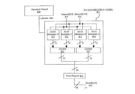
In summary, Figure 8 illustrates a circuit for performing multiply-add
operations on packed data according to one embodiment of the invention.
Operation control 800 processes the control signal for the multiply-add
instructions. Operation control 800 outputs signals on Enable 880 to control
Packed multiply-adder 801.
Packed multiply-adder 801 has the following inputs: Sourcel(63:0] 831,
Source2[63:0] 833. and Enable 880. Packed multiply-adder 801 includes four
16x16 multiplier circuits: 16x16 multiplier A 810, 16x16 multiplier B 811,
16x16 multiplier C 812 and 16x I 6 multiplier D 813. 16x 16 multiplier A 810
has
as inputs Sourcel[15:0] and Source2[15:0]. 16x16 multiplier B 811 has as
inputs
Sourcel [31:16] and Source2[31:16]. 16x 16 multiplier C 812 has as inputs
Sourcel [47:32] and Source2[47:32]. 16x 16 multiplier D 813 has as inputs
Sourcel[63:48] and Source2[63:48]. The 32-bit intermediate results generated
by
CA 02230108 1998-02-23
WO 97/08610 PCT/US96/12799
-20-
16x16 multiplier A 810 and 16x16 multiplier B 811 are received by adder 1350,
while the 32-bit intermediate results generated by 16x16 multiplier C 812 and
16x16 multiplier D 813 are received by adder 851.
The adder 850 and adder 851 add their respective 32-bit inputs. The
output of adder 850 (i.e., Result bits 31 through zero of the Result) and the
output of adder 851 (i.e., bits 63 through 32 of the Result) are combined into
the
64-bit Result and communicated to Result Register 871.
In one embodiment, each of adder 851 and adder 850 is composed of a
32-bit adder with the appropriate propagation delays. However, alternative
embodiments could implement adder 851 and adder 850 in tiny number of ways.
Performing the equivalent of this multiply-add instruction using the prior
art DSP processor described with reference to Table 1 requires one instruction
to
zero the accumulation value and four multiply accumulate instructions.
Performing the equivalent of this multiply-add instruction using the prior art
DSP processor described with reference to Table 2 requires one instruction to
zero the accumulation value and 2-accumulate instructions.
In one embodiment of the multiply-add unit 145 of the present invention,
each 16-bit multiplier used for the packed multiplication operations in the
present invention is implemented using a 2-bit Booth algorithm. The main
purpose of Booth algorithm in multipliers is to reduce the number of partial
products to be summed. Fewer partial products consequently reduces the
hardware and the area requirement for the multiplier. Table 5 below describes
a
common 16-bit multiplication process where 16 partial products are generated.
Each partial product is shifted to the left by one bit and contains either all
"0"
terms or the exact replica of the multiplicand, depending on whether the
respective bit of the multiplier is a "I" or a "0". A 32-bit result is
generated by
summing all 16 partial products slice by slice.
CA 02230108 1998-02-23
WO 97/08610 PCT/US96/12799
-21-
Table 5
x x x x x x x x x x x x x x x x 16-bit
multiplied
xxxxxxxxxxxxxxxx 16-bit
multiplier
xxxxxxxxxxxxxxxx pp0
x x x x x x x x x x x x x x x x ppl
xxxxxxxxxxxxxxxx pp2
x x x x x x x x x x x x x x x x pp3
x x x x x x x x x x x r_ x x x x pp4
xxxxxxxxxxxxxxxx pp5
xxxxxxxxxxxxxxxx pp6
x x x x x x x x x x x x x x x x pp7
xxxxxxxxxxxxxxxx pp$
x x x x x x x x x x x x x x x x pp9
x x x x x x x x x x x x x x x x ppl0
x x x x x x x x x x x x x x x x ppl l
x x x x x x x x x x x x x x x x ppl2
x x x x x x x x x x x x x x x x ppl3
xxxxxxxxxxxxxxxx ppl4
x x x x x x x x x x x x x x x x ppl5
xxxxxxx ~ ~ ~ ~ ~ xxxxxxx 32-bitt~t
On the other hand, the 2-bit Booth multiplier shown below in table 6
operates differently. In this case there are a total of 8 partial products and
each
partial product is 17 bits long. Every partial product has its own Booth
encoder
which dictates what the contents of the respective partial product. In
alternative
embodiments, other Booth encoder schemes could be used to select partial
products.
A typical 2-bit Booth encoder has five outputs, which are for zero, plus 1,
plus 2, minus 1, and minus 2 operations. Its truth table is given below in
Table
6.
CA 02230108 1998-02-23
WO 97/08610 1'CT/US96/12799
-22-
Table .
6
BOOTH = -2yk + yk +
yk -1
c+1 YK k-1 BOOTH
0 0 0 0 zero (Z)
0 0 1 1 plusl (P1)
0 1 0 1 plus 1 (P2)
0 1 1 2 plus2 (M2)
1 0 0 -2 minus2 (M2)
1 0 1 -1 minusl (Ml)
1 1 0 -1 minusl (Ml)
1 1 1 0 zero (Z)
As set forth in Table 6, yk+1, yk and yk-1 are the adjacent multiplier bits
in descending order of significance. Table 7 below, further describes the form
of
the partial products according to the Booth encoder outputs.
CA 02230108 1998-02-23
WO 97/08610 PCT/US96/12799
-23
Table 7
17-bit zero string
IF ZERO=1 then 0 0 0 0 0 0 0 0 0 0 0 0 0 0 0 0 0
n=0
16-bit multiplicand
IF PLUS 1=1 then 0 x x x x x x . x x x x x x x x x
n=0
16-bit multiplicand left shifted by 1
IF PLUS2=1 then x x x x x x x x x x x x x x x x 0
n=0
16-bit multiplicand complemented
IF MINUSl=1 then 1 X X X X X X X X X X X X X X
n=1
16-bit multiplicand complemented and shifted left by 1
IF MINUS Z=1 then X X X X X X X X X X X X X X X X 1
n=1
Instead of sign extending the partial products, a sign generate method is
used to reduce the number of Carry Same Address (CSA's) needed for partial
product reduction. Table 8 shows the sign generate method. The complement of
CA 02230108 1998-02-23
WO 97/08610 PCT/US96/12799
-24-
the sign bit of a partial product is prepended to the partial product. Two one
bits
are then prepended to the complement of the sign bit.
Table 8
Sign-extension method Sit?n-generate method
1
S 1 S 1 S 1 partial product 1 1 S 1 partial product
1
S2 S2 partial product 2 1 S2 partial product 2
partial product 3 1 S3 partial product 3
Table 9 below shows the 16-bit multiplication process used in one
embodiment of the present invention using the 2-bit Booth encoder and the sign
generate method to generate 8 partial products.
Table 9
x x x x x x x. x x. x x x x. x x x ~--16-bit multiplicand
x x x x x x x x. x x x x x x x. x X16-bit multiplier
1 Multiplicand Generated by multiplier biu
lx x x x x x x x x x x x x x x x~Booth (k=0):z,pl,ml,m2
n
lx x x x x x x x x x x x x x x x ~- Booth (k=2):z,pl,ml,m2
n
lx x x x x x x x x x x. x x x x x -~ Booth (k=4):z,pl,ml,m2
n
lx x x x x x x x x x x x x x x x -~ Booth (k=6):z,pl,ml,m2
n
lx x x x x x x x x x x x x x x x ~ Booth (k=8):z,pl,ml,m2
n
ix x x x x x x x x x x x x x x x Booth (k=10):z,pl,ml,m2
n
lx x x x x x x x x x x x x x x x Booth (k=12):z,pl,ml,m2
n
lx x x x x x x x x x x x x x x x Booth (k=14):z,pl,ml,m2
n
x x x x x x x x x x x x x x x x x x x x x x x x x x x x x x x x ~ 32-bit
result
In one embodiment, each Booth encoder contains 3 adjacent multiplier
bits (y0 is the least significant bit and y 15 is the most significant bit of
the
multiplier bits). The form of the partial product is defined by 17 selectors
and a
CA 02230108 1998-02-23
WO 97/08610 PCT/US96/12799
-25-
negate circuit connected to a particular Booth encoder. The data bits of the
selectors contain 2 adjacent multiplier bits, their compliments and Vcc (for
zero
operation). The selected outputs then go through a maze of partial product
reduction tree, commonly referred to as a Wallace tree.
Once the partial products are all selected then the summation of partial
products begins. The Wallace tree is made out of full adders and half adders.
Figures 9a-9e illustrate the Wallace tree performing the partial product
summation and reduction for one embodiment of the present invention, as
implemented by each of the four 16-bit multipliers in the multiply-add unit
145.
As illustrated, 8 partial products are reduced to 6 partial products, then to
4
partial products, then to 3 partial products, and then finally to 2 partial
products.
More specifically, as illustrated in Figures 9a-9e, the subscript numbers
in each row represent bits of a partial product (ase 15> as 15~ a I 4 - a0).
Each row
represents a separate partial product. Negh - nega represent the +1 part of a
2's
complement, for each partial product. As a result, if a certain Booth encoded
bit
of the multiplier is negative, that corresponding partial product's "neg" bit
is 1,
set forth in the next row.
In addition, as further illustrated in Figures 9a-9e, S<position><adder
number> t'epresents the sum portion of a carry-save adder. <adder number>
indicates to which row of adders sum belongs. Adders are numbered from top to
bottom of Figures 9a-9e. <position> indicates which bit position (0...31 )
this
adder operates. For example, S42 is the sum of a carry-save adder 2 that
corresponds to bit position 4.
C <position><level> represents the carry portion of a carry-save adder.
<level> indicates the respective row of adders for the carry. <position>
indicates
which bit position (0...31 ) this adder operates. A carry-save adder can be a
full
adder, or a half adder. A full adder adds 3 bits together. A half adder adds 2
bits.
Figures 9a-9e further illustrate implementation of the Sign-Generate
method as previously described. As illustrated, the Sign-Generate method
creates a '1 on bit position 16 in row above the first partial product row. In
the
last partial product row, if the most significant Booth encoding number is
negative, a 1 is created in a row below because the partial product is 2's
complemented. This process would typically require 10 rows instead of 8. The
CA 02230108 1998-02-23
WO 97/08610 PCT/US96/12799
-26-
more rows a multiplication has, the more hardware is needed to reduce the
partial
products into 2 numbers on which a carry-propagate adder can add.
Binary multiplication, however, is performed through addition. When
two numbers are added, the order of the numbers is irrelevant. The result is
the
same regardless of which number is the first number. This principle is used
throughout the Wallace tree to reduce the number of carry-saves needed.
Specifically, in one embodiment, the 1 in bit position 16 of the first row in
Figure 9a is moved down to bit position 16 in the last row of Figure 9, which
also contains negh. As a result, less hardware is needed to do the reduction
because fewer rows are used.
Figure 9b illustrates the result of the first level of reduction. The boxes
indicate which bits are operated on by carry-save adders. A number of bits are
moved around to fit everything in 6 rows. For example, bit dsel5 is moved to
the first row. csel5 is moved to a fifth row. A bit, however, should only be
moved up or down in the same bit position. From Figure 9b to Figure 9c, the
number of rows is reduced to 4. From Figure 9c to Figure 9e, the number of
rows is reduced to 3. Finally, one more row of carry-save adders reduces the
number of rows to 2, as shown in Figure 9e.
Figures l0a - l Of illustrate one embodiment of a circuit, comprised of full
adders and half adders, implementing the Wallace tree diagram illustrated in
Figures 9a-9e.
Figure 11 illustrates one embodiment of a block diagram of the unit.
There are 2 identical 16-bit multipliers illustrated. The multipliers could
perform
the multiply-add operation on either the 0-31 bit or the 32-63 bits. An
additional
2 16-bit multipliers would also be provided, very similar in structure to the
multipliers illustrated, to complete the multiply-add unit 145. As
illustrated,
each multiplier accomplishes a 16-bit multiplication resulting in 2 partial
products in 1.5 clock cycles. In the next half clock cycle, which is the low
phase
of the 34th clock, the 4 partial products generated by multipliers 1 1 10 and
1120
are summed again by a 4:2 CSA 1130. The control signal 1150 selects either the
partial product of the multiplier 1110 or the partial product generated at the
output of the 4:2 CSA 1130 (Sutures and coutres). The selected data is latched
along with the partial products of multiplier 1120. At the high phase of the
35th
clock, CPA 1140 generates a 32-bit result by adding the resultant partial
CA 02230108 1998-02-23
WO 97/08610 PCT/US96/12799
-27-
products. The final partitioning of the 32-bit sum is accomplished by a mux-
latch outside of the fub and the selected data is written back at the low
phase of
the 35th clock cycle.
In one embodiment, the multiply-add unit 145 operates with a 3 latency-1
throughput rule. Otherwise stated, the unit 145 requires 3 clock cycles to
complete its task every time an unpiped data stream is introduced to the
inputs.
All the inputs of the unit 145 are buffered, which offers very small
capacitance to
the outside world.
Even though the data is available at the inputs of unit 145 at the
beginning of 32L, the data may not be valid until 33H begins. Therefore, the
multiplication is assumed to start at the beginning of 33H. During 33H the
valid
and stable data on the multiplicand inputs flow through the delay elements and
get latched by latches 1160 and I 170, respectively. At the same time, the
data on
the multiplier inputs propagate through the input buffers and the Booth
encoders
1165 an 1175 and get latched by latches 1180 and 1 182. At this point, the
data
on both multiplier and multiplicand paths are perfectly synchronized with each
other. In 331, the data go through the bit selector array and a set of full
adders,
which forms the first part of the Wallace tree and becomes valid before the
setup
time for latches 1180 and 1182. The number of partial products at this point
is
reduced from 8 to 4. In 34H, the data goes through another set of full adders
which constitute the remainder of the Wallace tree and become valid and stable
at the end of 34H before getting latched by latches I 184 and 1186.
As previously explained, during 34L the data goes through 4:2
compressor 1130 (two full adders in series) and a 2-1 mux 1135 for the final
partial product selection. The data becomes valid at the end of 34L before
getting latched by latch 1190. During 35H, the two partial products at the
latch
1190 output are finally reduced to one sum vector. This sum vector gets
portioned and latched by a mux-latch boundary, latch 1195, outside of unit
145.
In 35L, the data is available for write-back operation.
As previously described, the previous multiply accumulate instructions
always add the results of their multiplications to an accumulation value. This
accumulation value becomes a bottleneck for performing operations other than
multiplying and accumulating (e.g., the accumulation value must be cleared
each
time a new set of operations is required which do not require the previous
CA 02230108 2000-02-24
-28-
accumulation value). This accumulation value also becomes a bottleneck if
operations,
such as rounding, need to be performed before accumulation.
In contrast, the disclosed multiply-add operation does not carry forward an
accumulation value. As a result, these instructions are easier to use in a
wider variety of
algorithms. In addition, software pipelining can be used to achieve comparable
throughput. To illustrate the versatility of the multiply-add instruction,
several example
multimedia algorithms are described below. Some of these multimedia algorithms
use
additional packed data instructions. The operation of these additional packed
data
instructions are shown in relation to the described algorithms. Of course,
other packed
data instructions could be used. In addition, a number of steps requiring the
use of
general purpose processor instructions to manage data movement, looping, and
conditional branching have been omitted in the following examples.
CA 02230108 1998-02-23
WO 97/08610 PCT/LTS96/12799
-29-
, 1) lVIultiplication of Complex Numbers
The disclosed multiply-add instruction can be used to multiply two
complex numbers in a single instruction as shown in Table 10a. As previously
described, the multiplication of two complex number (e.g., rl i 1 and r2 i2)
is
performed according to the following equation:
Real Component = r 1 ~ r2 - i 1 ~ i2
Imaginary Component = rl ~ i2 + r2 ~ i 1
If this instruction is implemented to be completed every clock cycle, the
invention can multiply two complex numbers every clock cycle.
Table l0a
Multinlv-Acid Snor~Pl Crn~r~P'7
rl t2 rl i 1 Source
1
r2 -t2 i2 r'? Source2
Real (lomponent: Imaginary Result
Component:
rl t'2-i rl i~+r2i 1
1 i2 1
As
another
example,
Table
lOb
shows
the
instructions
used
to
multiply
together
three
complex
numbers.
Multinlv-Arlrl Scmr~Pl Snmrr-P7
rl il rl il Sourcel
r2 -i2 i2 r'? Source2
Real Componentl: Imaginary Resultl
rlr2-ili2 Componentl:
rli~+r~il
CA 02230108 1998-02-23
WO 97/08610 PCT/US96/12799
-30-
Packed Shift Right Source), Source2 ,
Real Component) Imaginary Result)
Component)
16
Real Imaginary Result2
Component) Component)
Table lOb
Pack Result2, Result?
Real Imaginary Result?
Component Component
1 1
Real Imaginary Result2
Component) Component)
Real Imaginary Real Imaginary Result3
Component Component Component Component
1 1 1 1
Muhinlv-Add Result3. Source3
Real Imaginary Real Imaginary Result3
Component) Component Component Component)
: ) : ) :
rlr2-ili2 rli~+r?il rlr2-ili~ rli?+r~il
r3 -i~ i3 r3 Source3
Real Component? Imaginary Result4
Components
2) Multiply Accumulation Operations
CA 02230108 1998-02-23
WO 97/08610 PCT/CTS96/12799
-31-
The disclosed multiply-add instructions can also be used to multiply and
accumulate values. For example, two sets of four data elements (Al-4 and BI_4)
may be multiplied and accumulated as shown below in Table 11. In one
embodiment, each of the instructions shown in Table 6 is implemented to
complete each clock cycle.
Table 11
Multinlv-Acjrl ~rn~r~Pl ~nmrrP7
0 0 A I A ~ Source
1
0 0 B I B? Source?
0 ( A I B I Result
+A2B2 I
Multinlv-Arm CnmrrP'~ CnmrrPd
0 0 A3 A~ Source3
0 0 B~ B4 Source4
0 I A3A,~+B3B4 Result2
CA 02230108 1998-02-23
WO 97/08610 PCT/US96/12799
-32-
Unpacked Add Resultl, Result2 ,
0 AlBI+A2B2 Resultl
0 A3A4+B3Bq Result2
0- -~ A1B1+A2B2+A3A4+B3B4 Result3
I
If the number of data elements in each set exceeds 8 and is a multiple of
4, the multiplication and accumulation of these sets requires fewer
instructions if
performed as shown in Table 12 below.
Table 12
MultiDlv-Add Sourcel. Source2
A1 A2 A3 A4 Sourcel
Bl B2 B3 B4 Source2
A1B1+A2B2 A3B3+A4B4- Resultl
-I
Multiplv-Add Source3, Source4
AS A( A~ Ag Source3
BS B~, B~ Bg Source4
ASBS+A~B6 A~B7+AgBg Result2
I
CA 02230108 1998-02-23
WO 97/08610 PCT/US96/12799
-33
Packed Add Resultl, Result2
A1B1+A2B2 A3B3+Aq.B4 Resultl
ASBS+A~B6 A~B~+AgBg Result2
A1B1+A2B2+ASBS+A(B6 A3B3+A4B4+A~B~+AgBg Result3
lJnnack T-link Recalt~ Cn»rrPS
A1B1+AZB2+ASBS+A(~B~ A3B3+A4B.~+A~B~+AgBg Result3
0 0 Sources
0 ~ A 1 B 1+A~B~+A5B5+A~B~Result4
Ilnnack l.nm.~ RPCmIt'~ Crn~rrPS
AIBl+A2B?+A$B5+A(,B(~ A3B3+A,~B~+A~B7+ARBg esult3
R
0 U Sources
0 I A3B3+A4Bq.+A7B~+AgBg Results
Packed Add Result4_ Results
0 AIBI+A~B2+ASBS+A~B~ Result4
0 A3B3+A4Bq+A~B~+AgBg Results
0 I TOTAL Result6
CA 02230108 1998-02-23
WO 97/08610 PCT/US96/12799
-34-
As another example, Table 13 shows the separate multiplication and
accumulation of sets A and B and sets C and D, where each of these sets
includes
2 data elements.
Table 13
Multiply-Add Sourcel, Source2
A1 A~ C1 C? Sourcel
B 1 B2 D 1 D~ Source?
A1B1+A2B2- ~_C]D1+C2D? Ressltl
- ~
As another example, Table 14 shows the separate multiplication and
accumulation of sets A and B and sets C and D, where each of these sets
includes
4 data elements.
Table 1.~
Multiply-Add Source 1, Source?
A1 A2 C1 C? Sourcel
B 1 B2 D 1 DZ Source?
_. A1B1+A2B2_ C1D1+C2D2 Resultl
~ I
CA 02230108 1998-02-23
WO 97/08610 PCT/US96/12799
-35-
Multiply-Add Source3. Source4
A3 A4 C3 ' C4 Source3
B3 B4 D3 D4 Source4
A3B3+A4B4 Result2
C3D3+C4D4
Packed Add Retulrl_ Rewlr?
AlBl+A2B2 C1D1+C?D? Resultl
A3B3+A4B4 C3D~+C4D4 Result2
A I B I+A2B2+A3B3+A4B4 C1 D I+C?D?+C3D3+C4D.~Result6
I
3) Dot Product Algorithms
Dot product (also termed as inner product) is used in signal processing
and matrix operations. For example, dot product is used when computing the
product of matrices, digital filtering operations (such as FIR and IIR
filtering),
and computing correlation sequences. Since many speech compression
algorithms (e.g., GSM, 6.728, CELP, and VSELP) and Hi-Fi compression
algorithms (e.g., MPEG and subband coding) make extensive use of digital
filtering and correlation computations, increasing the performance of dot
product
increases the performance of these algorithms.
The dot product of two length N sequences A and B is defined as:
N-1
Reault --~~ Ai ~ Bi
I=0
. Performing a dot product calculation makes extensive use of the multiply
accumulate operation where corresponding elements of each of the sequences are
CA 02230108 1998-02-23
WO 97/08610 PCT/US96/12799
-36-
multiplied together, and the results are accumulated to form the dot product
result.
The dot product calculation can be performed using the multiply-add
instruction. For example if the packed data type containing four sixteen-bit
elements is used, the dot product calculation may be performed on two
sequences each containing four values by:
1) accessing the four sixteen-bit values from the A sequence to generate
Sourcel using a move instruction;
2) accessing four sixteen-bit values from the B sequence to generate Source2
using a move instruction; and
3) performing multiplying and accumulating as previously described using a
multiply-add, packed add, and shift instructions.
For vectors with more than just a few elements the method shown in
Table 9 is used and the final results are added together at the end. Other
supporting instructions include the packed OR and XOR instructions for
initializing the accumulator register, the packed shift instruction for
shifting off
unwanted values at the final stage of computation. Loop control operations are
accomplished using instructions already existing in the instruction set of
processor 109.
4) Discrete Cosign Transform Algorithms
Discrete Cosine Transform (DCT) is a well known function used in many
signal processing algorithms. Video and image compression algorithms, in
particular, make extensive use of this transform.
In image and video compression algorithms, DCT is used to transform a
block of pixels from the spatial representation to the frequency
representation. In
the frequency representation, the picture information is divided into
frequency
components, some of which are more important than others. The compression
algorithm selectively quantifies or discards the frequency components that do
not
adversely affect the reconstructed picture contents. In this manner,
compression
is achieved.
There are many implementations of the DCT, the most popular being
some kind of fast transform method modeled based on the Fast Fourier
Transform (FFT) computation flow. In the fast transform, an order N transform
is broken down to a combination of order N/2 transforms and the result
CA 02230108 1998-02-23
WO 97/08610 PCT/US96/12799
-37-
recombined. This decomposition can be carried out until the smallest order 2
transform is reached. This elementary 2 transform kernel is often referred to
as
the butterfly operation. The butterfly operation is expressed as follows:
X = a*x + b*y
Y = c*x - d*y
where a, b, c and d are termed the coefficients, x and y are the input data,
and X
and Y are the transform output.
The multiply-add allows the DCT calculation to be performed using
packed data in the following manner:
1 ) accessing the two 16-bit values representing x and y to generate
Sourcel (see Table 10 below) using the move and unpack instructions;
2) generating Source2 as shown in Table 10 below -- Note that Source2
may be reused over a number of butterfly operations; and
3) performing a multiply-add instruction using Source 1 and Source2 to
generate the Result (see Table 15 below).
Table 15
x y x y ~Sourcel
b c -~Source2
a~ x+b ~ y c~ x-d ~ y Source3
In some situations, the coefficients of the butterfly operation are I . For
these
cases, the butterfly operation degenerates into just adds and subtracts that
may be
performed using the packed add and packed subtract instructions.
An IEEE document specifies the accuracy with which inverse DCT
should be performed for video conferencing. (See, IEEE Circuits and Systems
Society, "IEEE Standard Specifications for the Implementations of 8x8 Inverse
Discrete Cosine Transform," IEEE Std. 1180-1990, IEEE Inc. 345 East 47th St.,
NY, NY 10017, USA, March 18, 1991 ). The required accuracy is met by the
CA 02230108 1998-02-23
WO 97/08610 PCT/US96/12799
-38-
disclosed multiply-add instruction because it uses 16-bit inputs to generate
32-bit
outputs.
In this manner, the described multiply-add instruction can be used to
improve the performance of a number of different algorithms, including
algorithms that require the multiplication of complex numbers, algorithms that
require transforms, and algorithms that require multiply accumulate
operations.
As a result, this multiply-add instruction can be used in a general purpose
processor to improve the performance of a greater number algorithms than the
described previous instructions.
While the invention has been described in temrts of several embodiments,
those skilled in the art will recognize that the invention is not limited to
the
embodiments described. The method and apparatus of the invention can be
practiced with modification and alteration within the spirit and scope of the
appended claims. The description is thus to be regarded as illustrative
instead of
limiting on the invention.