Note: Descriptions are shown in the official language in which they were submitted.
-.
CA 02230250 1999-11-08
BACKGROUND OF THE INVENTION
In general, two wire, low current loop circuits are used with a variety of
devices, for
example, flow measurement devices. These loop circuits typically include a
loop current
regulating circuit which varies the current in the loop, generally from 4 to
20 mA, according to a
signal received from the associated device. For example, when the loop circuit
is used with a
flow measurement device, such as a flow meter in a typical process control
loop, the flow meter
provides a signal ranging from 4 to 20 mA which represents the measured flow
rate. This signal
is then provided to a controller, which compares the signal received from the
measurement
device to a signal which represents a desired flow rate, or "set point." The
controller calculates a
corrective signal (which also may be a 4 to 20 mA signal) that is output to a
control device such
as a control valve. The control device exerts an influence on the process in
response to the
received corrective signal to bring the process to the desired flow rate.
The device connected to the loop circuit may include various electronic
components such
as a microprocessor or display device. It is desirable to power these
electronic components via
the loop circuit, rather than powering the electronic components via a
separate power circuit,
thereby reducing installation and maintenance costs. However, these electronic
components
generally require high current, low voltage as opposed to the low current,
high voltage typically
H: 207620(IG7801!.DOC)
CA 02230250 1998-03-30
supplied by the loop circuit. Moreover, the electronic components of the
associated device often
communicate digitally over the loop circuit via Frequency Shift Key ("FSK")
signals. Using the
4 to 20 mA circuit for communication further reduces wiring requirements, in
turn providing
additional cost reductions. Several FSK protocols exist, including the HART
protocol or other
protocols which modulate the loop current at audio frequencies. Accordingly,
efficient low
powered power management components are needed to regulate the distribution of
energy to the
electronic components without introducing noise onto the loop circuit that can
interfere with the
digital communication or presenting a complex impedence to the transmitting
source which may
attenuate or distort the signal.
l0 Figure 1 illustrates a typical prior art loop current regulating circuit
100. The prior art
loop current regulating circuit 100 is connected between positive loop voltage
+LOOP and
negative loop voltage -LOOP. The loop current regulating circuit 100 includes
a current control
circuit 112 and a current compare circuit 113. The current compare circuit 113
senses an actual
current on the loop and compares it to a current demand signal 114 received
from an associated
15 device (not shown). The demand signal 114 provided by the associated device
is in response to a
sensed process variable. For example, for an associated device which measures
the flow rate of a
fluid such as a flow meter, the demand signal provided to the current compare
circuit 113
represents the sensed flow rate. The current compare circuit 113 then signals
the current control
circuit 112 to increase or decrease the loop current to meet the current
demanded by the current
2o demand signal 114. The current control circuit 112 utilizes a linear shunt
regulator to vary the
current in the loop in accordance with the signal received from the current
compare circuit 113
H: 207620(4G7801!.DOC)
CA 02230250 1998-03-30
and to form a pre-regulator circuit for controlling start-up functions at
initial application of
power.
The linear shunt regulator includes a transistor 115, a zener diode 116, and a
resistor 117.
The transistor 115 operates linearly and becomes more or less conductive based
on the signal
from the current compare circuit 113. If the loop current needs ~o be
increased, the transistor 115
becomes more conductive. As the transistor 15 becomes more conductive, the
voltage at node
118 increases. When the voltage at node 118 reaches approximately 7 volts, the
zener diode 116
will turn on. At this point, all current in excess of the demanded loop
current will sink to ground
through the zener diode 116.
However, the prior art loop current regulating circuit 100 provides inexact
current control
at best. In the prior art circuit only one active device is utilized and the
path to ground is not
controlled by the active device. Rather, the path to ground is through the
zener diode 116 and
therefore, is only indirectly controlled. Thus, precise current control is not
possible. Moreover,
the current control of the loop current regulating circuit 100 is not smooth,
because of the abrupt
nature of the linear shunt regulator: the zener diode 116 is either on or off.
Another problem
created by the prior art circuit is that the current control circuit creates a
complex impedance.
This complex impedance can distort FSK signals, if the circuit is used with a
device that
transmits and receives FSK signals over the loop circuit. If the digital
communications signals
cannot be reliably transmitted and received over the loop circuit, the cost
advantage gained
2o through reduced wiring is lost.
Further, it is desirable to power peripheral electronics of an associated
device from the
loop circuit 100 at node 118. However, the prior art loop current regulating
circuit 100 causes
4
H: 207620(4G7801!.DOC)
CA 02230250 1998-03-30
several problems vt~hen used to provide power to an associated device. First,
the power drain is
great due to the loss associated with the zener diode 116. Thus, the prior art
loop current
regulating circuit 100 is very inefficient. Additionally, the maximum power
provided to any
associated device is limited, because the voltage at node 118 is limited to a
maximum of
approximately 7 V by the zener diode 116. Therefore, the loop current
regulating circuit 10
provides poor power amplification. Moreover, if FSK signals are transmitted
and received using
the prior art circuit, noise can be introduced onto the loop by the FSK
circuits connected to the
loop current regulating circuit 100, which regulates power to the associated
device.
Finally, devices employed on low current loop circuits are often used in
hazardous areas
where electrical energy or sparks could cause disastrous ignition of
surrounding explosive gasses
or particles. Accordingly, the power management components must be designed to
meet the
standards set forth for an Intrinsically Safe device. Such devices receive
their operating voltage
through energy limiting barriers, and must be specially constructed to reduce
or eliminate
electrical discharges capable of causing combustion of the surrounding
materials.
15 Thus, a need exists for an improved power management circuit that overcomes
the
referenced and other limitations of prior art power management circuits.
SUMMARY OF THE INVENTION
The present invention overcomes the described and other limitations of
traditional power
2o management circuits by providing an improved power management circuit. In
one aspect of the
invention, a loop current regulating circuit produces a demanded current in a
loop current circuit
that contains an actual current and provides power to an associated device.
The power
H: zo~ezaac~so~,.noc~
CA 02230250 1998-03-30
management circifit includes a current compare circuit which receives a
demanded current signal
and compares the actual current to the demanded current signal and produces a
control signal.
An active upper device receives the control signal and conducts based on the
control signal to
produce the demanded current. An active lower device receives the control
signal and conducts
based on the control signal to produce the demanded current. A voltage is
produced at an
intermediate node where the active upper device and the lower device are
electrically coupled,
and the voltage at the intermediate node is able to float to the voltage
necessary to provide the
demanded current.
In another aspect of the current invention, the loop current regulating
circuit includes a
to receive FSK circuit and a transmit FSK circuit coupled to the loop current
circuit. In yet another
aspect of the invention, a power regulating circuit is further included which
receives the voltage
from the intermediate node and outputs at least one lesser voltage to an
associated device.
In another embodiment of the invention, a method of creating a demanded
current in a
loop current circuit containing an actual current comprising the steps of
sensing the actual current
I S on the loop current circuit, comparing the actual current to a signal
representation of the
demanded current, and creating a control signal from a comparison of the
actual current and the
signal representation of the demanded current. Further, the method of the
invention includes
creating a demanded current by controlling an upper active device and a lower
device with the
control signal such that voltage at an intermediate node between the upper
active device and the
20 lower device can vary as necessary to attain the demanded current. In
another aspect, the method
also includes stepping down the voltage at the intermediate node and supplying
the voltage to an
associated device.
6
H: 207620(4G7801!.DOC)
CA 02230250 1998-03-30
BRIEF DESCRIPTION OF THE DRAWINGS
Figure 1 illustrates a simplified prior art loop current control circuit.
Figure 2 illustrates an overview of the power management circuit of the
present
invention.
Figure 3 illustrates a simplified embodiment of the loop current regulating
circuit of the
present invention, highlighting the current control circuit.
Figure 4 illustrates a simplified embodiment of the loop current regulating
circuit of the
present invention, highlighting the current compare circuit.
1o Figure 5 is a schematic diagram of an exemplary embodiment of the loop
current
regulating circuit.
Figure 6 illustrates a simplified embodiment of the power regulating circuit
of the present
invention.
Figure 7 illustrates a circuit diagram of an exemplary embodiment of the power
15 regulating circuit.
Figure 8 illustrates a circuit diagram of an embodiment of the power fail
detect delay
circuit of the present invention.
Figure 9 illustrates a circuit diagram of an embodiment of the FSK receive
circuit of the
present invention.
2o Figure 10 illustrates a circuit diagram of an embodiment of the loop EMC
filter and
intrinsically safe protection circuit of the invention.
H: 207620(4G7801!.DOC)
CA 02230250 1998-03-30
DETAILED DESCRIPTION OF THE INVENTION
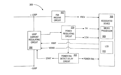
Turning to the drawings and in particular, to Figure 2, an exemplary power
management
circuit 300 in accordance with the present invention is illustrated. In
general, the power
management circuit 300 includes an improved loop current regulating circuit
200 connected
between positive loop voltage +LOOP and negative loop voltage -LOOP, an FSK
receive circuit
302 coupled between +LOOP and an associated device 308, a power regulating
circuit 220
connected between the loop current regulating circuit 200 and associated
device 308, and a
power fail detect delay circuit 304 connected between power regulating circuit
220 and loop
current regulating circuit 200. Associated device 308 may include peripheral
electronic devices;
to an exemplary embodiment includes a microprocessor 309 and a liquid crystal
display (LCD) 310.
Examples of other peripheral electronics include memory devices such as flash
read only
memory (ROM) and static random access memory (RAM).
In an embodiment of the invention, the associated device 308 is an instrument
for
measuring a process variable, such as a flow meter. In alternate embodiments,
the associated
15 device 308 may comprise a pressure or level transducer, for example.
Associated device 308
generates a current demand signal VIDMD corresponding to a measurement of the
process
variable which is input to the loop current regulating circuit 200. The
improved loop current
regulating circuit 200 functions to control the loop current in response to
current demand signal
VIDMD such that the loop current represents the measurement of the process
variable. For
2o example, in a typical process control loop, the loop current ranges from 4
to 20 mA. Thus, for an
associated device 308 such as a flow meter, a loop current of 4 mA may
represent a minimal
measured flow rate, while a loop current of 20 mA may represent a maximum flow
rate.
8
H: 207620(4G78011.DOC)
CA 02230250 1998-03-30
As discussed in the Background of the Invention section herein above, it is
desirable to
power the associated device's 308 peripheral devices via the loop circuit.
Hence, the power
regulating circuit 220 of power management circuit 300 further functions to
convert the high
voltage, low current loop power to the low voltage, high current power source
required by the
peripheral electronics. In the exemplary embodiment of Figure 2, the power
management circuit
300 converts the 4 to 20 mA loop at 24 volts (nominal) to a 3.3 volt power
source for the
microprocessor 309. In addition, the power regulating circuit 220 provides +5
volts for the LCD
display 310.
Further, modulating communications to and from associated device 308 on the 4
to 20
mA loop rather than providing a separate pair of wires solely for
communications reduces the
amount of wiring necessary, in turn reducing installation and maintenance
costs for a typical
implementation of a process control loop. Thus, the associated device 308
transmits and receives
digital communications via FSK signals over the 4 to 20 mA loop. The FSK
receive circuit 302
extracts the digital communications signal FRCV from the +LOOP and provides it
to the
associated device 308. Transmitted digital communications FXMT are provided
from the
associated device 308 to the loop current regulating circuit 200, which
modulates the FXMT
signal onto the 4 to 20 mA loop.
The exemplary power management circuit 300 also includes a power fail detect
delay
circuit 304, which is used to increase the power supplied by the loop current
regulating circuit
200 to the power regulating circuit 220 when the power regulating circuit 220
indicates that its
load is drawing more power than it is receiving. Further, the power fail
detect delay circuit 304
9
H: 207620(4G7801!.DOC)
CA 02230250 1998-03-30
will alert the microprocessor of the associated device 308 that the power
regulating circuit 220 is
not receiving enough power.
Referring now to Figure 3 and Figure 4, the improved loop current regulating
circuit 200
in accordance with the present invention is illustrated. The loop current
regulating circuit 200 is
connected between positive loop voltage +LOOP and negative loop voltage -LOOP,
and includes
a current compare circuit 202 and a current control circuit 204. The main
components of the
current control circuit 204 are shown in Figure 3, and Figure 4 illustrates
the functional areas of
the current compare circuit 202. The current compare circuit 202 senses the
actual current on the
loop and compares it to a current demand signal VIDMD which is received from
associated
1 o device 308. Based on the comparison between the actual loop current and
the current demand
signal VIDMD, a control signal is generated and sent to the current control
circuit 204. The
current control circuit 204 regulates the current in the loop circuit based on
the control signal
received from the current compare circuit 202.
An upper active device 206 and a lower active device 208 are at the heart of
the current
15 control circuit 204, illustrated in Figure 3. The upper active device 206
has an input node 210,
an output node 211, and a control node 212, and the lower active device 208
also has an input
node 213, an output node 214, and a control node 215. Both the upper active
device 206 and the
lower active device 208 operate linearly. In one embodiment of the present
invention the upper
and lower active devices 206 and 208 are metal oxide semiconductor (MOS) field
effect
2o transistors (FET).
The upper active device 206 is controlled via the control signal from the
current compare
circuit 202 at the control node 212. The lower active device 208 is controlled
via the control
1o
H: zo~e2aac~em ~.noc>
CA 02230250 1998-03-30
signal from the cuirent compare circuit 202 at the control node 215. Because
both active devices
206 and 208 operate linearly, the active devices 206 and 208 will conduct more
or less depending
on the control signal from the current compare circuit. The upper and lower
active devices 206
and 208 are biased such that when the upper active device 206 and the
associated device 308
(and peripherals) cannot satisfy the current demand, the lower active device
208 conducts. When
the lower active device 208 conducts, current is sunk to ground at output node
214.
Power is provided to power regulating circuit 220 at intermediate node 218.
Intermediate
node 218 is formed between the output node of the upper active device 206 and
the input node
213 of the lower active device. Because the lower active device 208 is
utilized to sink current to
to ground, the voltage at intermediate node 218 is allowed to float.
Therefore, the voltage at
intermediate node 218 is allowed to reach whatever voltage is necessary to
provide the demanded
current and is not held at an artificial voltage as with the prior art. This
configuration affords for
a smooth control of current. Moreover, only as much current as is necessary is
sunk to ground
using the lower active device 208, thereby providing an efficient circuit.
Additionally, the
15 control of the current utilizing the current control circuit 204 is much
more precise than the prior
art circuit shown in Figure 1.
Figure 4 illustrates the major components of the current compare circuit 202
of loop
current regulating circuit 200. As explained above, the loop current
regulating circuit 200 is
made up of the current control circuit 204 and the current compare circuit
202. The current
20 compare circuit 202 includes a loop current sense circuit 501, a current
demand buffer 502, a
summing junction 505, and a control integrator .503.
11
H: zo~62aac~em,.noc~
CA 02230250 1998-03-30
The current received from the low current source -LOOP is sensed by the loop
current
sense circuit 501. The current demand signal VIDMD from associated device 308
is buffered in
the current demand buffer 502. The current demand signal VIDMD represents the
desired loop
current. The sensed current from the loop current sense circuit 501 is
compared to the current
demand signal VIDMD at summing junction 505, which generates an error signal
that is output
to the control integrator 503. The control integrator 503 receives the signal
from the summing
junction 505 and the transmit FSK signal FXMT from the associated device 308.
The transmit
FSK signal FXMT and the signal from summing junction 505 are integrated by
control integrator
503. The output of control integrator 503 is input to the current control
circuit 204, which
to adjusts the loop current accordingly. Further, the current control circuit
204 supplies power to
the power regulating circuit 220 and as necessary dissipates excess power to
ground.
An example circuit layout for loop current regulating circuit 200 is shown in
Figure 5.
The loop current sense circuit 501 includes a sense resistor 602, which may
comprise two
resistors in parallel. All current is forced through the sense resistor 602
because one side of the
15 loop sense resistor 602 is connected to -LOOP voltage and the other side is
connected to local
ground 606, which creates a voltage that is supplied to summing junction 505
through resistor
608. The other input to the summing junction 505 is the output of the current
demand buffer 502
through a resistor 614. The current demand buffer 502 includes a capacitor
610, an operational
amplifier 611 and a resistor 612. The result is the voltage across the sense
resistor 602 being the
20 same as the current demand voltage, but of negative polarity. In the
exemplary embodiment
illustrated in Figure 5, the VIDMD signal originates in a digital to analog
converter circuit (not
12
H: zm6zo~ac~son.noc>
CA 02230250 1998-03-30
shown) on the associated device 308 microprocessor 309 circuit board. It is
scaled and biased to
create a loop current ranging from 3.85 mA to 24.7 mA.
A filter comprising a capacitor 616, a resistor 618 and a capacitor 620 is
coupled to the
summing junction 505, and operates to filter the VIDMD signal as output from
summing
junction 505 and to maintain smooth control, transient voltage rejection and
proper impedance to
the FSK signals. The control integrator 503 includes an operational amplifier
622, a capacitor
623 and a resistor 624. At the junction 625 formed by resistor 626 and
resistor 627/capacitor
628, the FSK transmit signal FXMT is injected onto the filtered signal
received from the
summing junction 505 and both are input into the operational amplifier 622 of
the control
1o integrator 503.
The output of the control integrator 503 is connected to the base of a reach
up active
device 630. In the embodiment illustrated in Figure 5, the reach up active
device 630 is an NPN
transistor. As the control signal output from the control integrator 503
increases, transistor 630
increasingly conducts, causing its collector voltage to go low. The collector
of transistor 630 is
15 coupled to control nodes 212 and 215 of upper and lower active devices 206
and 208,
respectively. In the embodiment of Figure 5, upper and lower active devices
206 and 208
comprise P-channel enhancement metal oxide semiconductor field effect
transistors (E-
MOSFET), with control nodes 212 and 215 comprising the gates of MOSFETs 206
and 208,
respectively. The low at the collector of transistor 630 pulls down the gate
212 of upper active
2o device 206 and the gate 215 lower active device 208. The reach up active
device 630, upper
active device 206, and lower active device 208 aperate linearly. Thus, as the
collector of the
reach up active device 430 goes lower, the control nodes 212 and 215 of the
upper active device
13
H: 2o~ezaac~son.noc~
CA 02230250 1998-03-30
206 and lower active device 208 are pulled down. In turn, when the control
signal output from
the control integrator 503 decreases, the reach up active device 630 conducts
less, causing the
upper active device 206 and the lower active device 208 to conduct less.
The control node 212 of the upper active device 206 is pulled up by a resistor
450 and is
protected from excessive voltage by a zener diode 452. The gate of the lower
active device 208
is pulled up by a resistor 456 and is automatically protected against
excessive voltage drop by the
combination of zener diode 452 and an emitter resistor 457 of the transistor
630. A capacitor 458
is connected in parallel with the emitter resistor 457 in order to create a
zero in the response of
the loop circuit. A source resistor 448 of the lower active device 208 adds
some negative
l0 feedback to the lower active device 208.
To summarize the operation of the loop current regulating circuit 200 as
embodied in
Figure 5, if the current through the loop current sense circuit 501 decreases,
the voltage across it
becomes less negative (with respect to ground), which causes the summing
junction 505 to go
positive, as does the control integrator 503 output. This increases conduction
through reach up
15 transistor 630 causing its collector voltage to decrease. The upper active
device 206 admits more
loop voltage and, if necessary, the lower active device 208 sinks more
current. Current increases
through sense resistors 602 and 604, causing the input to summing junction 505
to go negative
which restores the balance at summing junction 505.
Referring now to Figure 6, the primary components of power regulating circuit
220 are
2o illustrated in a simplified block diagram. Power regulating circuit 220
includes a linear regulator
644 and a switching regulator 646. Loop voltage is presented to linear
regulator 644 and
switching regulator 646 from the current control circuit 204 through a filter
647. Additionally,
14
H: 207620(4G7801!.DOC)
CA 02230250 1998-03-30
positive loop voltage +LOOP is supplied to linear regulator 644. In an
embodiment of the
invention, power regulating circuit 220 provides the required low voltage,
high current supply for
the microprocessor 309 and LCD 310 of associated device 308, and additionally
powers the low
power detect delay circuit 304. In the exemplary embodiment illustrated in
Figure 6, the power
regulating circuit 220 provides, inter alia, a high current supply voltage Vcc
of 3.3 volts for
microprocessor 310. This conversion from the low current, high voltage 4 to 20
mA loop occurs
in the switching regulator 646, and a mathematical example of the conversion
is as follows:
Loop voltage = 23 volts, and Loop current = 4 mA (worst case). Thus, power
available =
0.092 watts:
Power = voltage * current = 23 volts * 4 mA = 0.092 watts
A switching regulator such as switching regulator 646 of the embodiment
illustrated in Figure 6
typically is about 75% efficient, therefore, realized output power is about
0.069 watts (0.092
0.75). For a Vcc of 3.3 volts, the available current is 20.9 mA:
Current = Powerlvoltage = 0.069/3.3 = 20.9 mA
An exemplary circuit layout of power regulator circuit 220 is illustrated in
Figure 7. In
the exemplary embodiment of Figure 7, an LT1120A Micropower Regulator from
Linear
Technology is used as the linear regulator 644. The pin functions for the
exemplary linear
regulator 644 are as follows:
Pin Function
1 ground
2 feedback
3 shutdown (not
used)
4 main output
5 input supply
6 2.5 v reference
7 comparator output
8 comparator input
H: 207620(4G7801!.DOC)
CA 02230250 1998-03-30
The linear regulator 644 receives the +LOOP voltage through a filter formed by
resistor
662 and capacitor 664 as its input supply. The linear regulator 644 provides
an output +VLCD
of 5 volts, which powers LCD 310 of associated device 308 and the low power
detect delay
circuit 304. The output of the linear regulator 644 is filtered by a capacitor
666. The linear
regulator 644 output +VLCD is fed back through resistors 667 and 668 and a
capacitor 669.
The linear regulator 644 includes a 2.5 volt reference source, and an open
collector
voltage comparator. The voltage comparator which may be used to detect when
input voltage is
below a predetermined level. The voltage created in loop current regulating
circuit 200 at
1o intermediate node 218 is passed through a filter 647 comprising a resistor
635, capacitors 636,
637, 638 and 639, and inductors 640 and 641 and provided to the linear
regulator 644 comparator
input through a resistor 643. If the input voltage falls below the
predetermined level, the linear
regulator 644 comparator output provides a shut down signal SHTDWN which may
be fed back
to the switching regulator 646 through a diode 671 to shut it down. If the
shut down signal
15 SHTDWN signal is used, it is also fed back to the linear regulator 644
through resistor 670.
The voltage from intermediate node 218 is passed through filter 647 to the
switching
regulator 646. In one embodiment, the switching regulator 646 is a Linear
Technology LT1111
Micropower DC/DC Converter. The pin functions for the exemplary linear
regulator 644 are as
follows:
Pin Function
current limit
2 input supply voltage
3 collector of internal power
transistor
4 regulator output
ground
16
H: 20T620(4G780I!.DOC)
CA 02230250 1998-03-30
6 comparator output
7 comparator input
8 feedback
Filter 647 prevents transients from getting into switching regulator 646 and
also prevents
switching and load transients from being reflected into the 4 to 20 mA loop.
The voltage from
the filter 647 provides the input supply voltage and is also supplied through
a resistor 642 to the
current limit input. Moreover, capacitors 636, 637, 638, and 639 of filter 647
store energy
received from node 218. This energy can be used by the switching regulator 646
if the power
provided by the current control circuit 204 is insufficient for the load of
the switching regulator
646.
An internal voltage comparator of the switching regulator 646 is used to
ensure that the
1o input voltage from the current control circuit 204 is sufficient. The
voltage comparator of the
switching regulator 646 compares the voltage between resistor 674 and resistor
672 with the
internal reference voltage (1.25 volts) of switching regulator 646. A small
positive feedback to
prevent oscillation is provided to the comparator by a resistor 680. If the
voltage at the input of
the switching regulator 646 falls below approximately 9.6 volts, the output of
the switching
15 regulator 646 comparator goes low. When the output of the comparator goes
low, a power fail
warn signal *PFW is asserted which acts as an interrupt to the microprocessor
of the associated
device 308. The resistor 678 acts as pull up resistor for the power fail warn
signal *PFW.
The output of the switching regulator is snubbed by a Schottky diode 682 and
filtered by
an inductor 684 and a capacitor 686 to create a voltage +VS. This voltage +VS
is input back into
2o the feedback input of the switching regulator 646 via a divider formed by a
resistor 692 and a
resistor 694, which are scaled to cause +VS to be +3.3 volts. The voltage +VS
is filtered by an
t7
H: 207620(4G7801!.DOC)
CA 02230250 1998-03-30
inductor 688 and a capacitor 690, resulting in the desired voltage +VCC of
3.3V. The voltage
+VCC is then used to power the microprocessor and other electronic circuits of
the associated
device 308.
Referring now to Figure 8, an embodiment of the power fail detect delay
circuit 304 is
shown. The power fail warn signal *PFW from the switching regulator 646 is
input into a
comparator 702. The comparator 702 compares the power fail warn signal *PFW
with the
reference voltage VR2 of the linear regulator 644. If *PFW is asserted (low),
then the output of
the comparator 702 goes low. This discharges a capacitor 704 through a
resistor 706 and a zener
diode 708. Resistor 710 is short circuited by diode 708. In an embodiment of
the invention, one
to half of an LMC6762 dual comparator provides the comparator 702.
The capacitor 704 is connected to a Schmidt Trigger 712 comprised of a
comparator 714,
a resistor 716, and a resistor 718. In the embodiment illustrated in Figure 8,
one half of an
LMC6762 dual comparator provides the comparator 714 for the Schmidt trigger
712. The output
of the comparator 714 is connected to a transistor 720 and through a resistor
724, to a NAND
15 gate 722. An emitter resistor 721 is coupled between the transistor 720 and
ground. When the
capacitor 704 discharges, the output of the comparator 714 goes high. Because
the capacitor 704
takes about 5 milliseconds to discharge, the comparator 714 goes high
approximately 5
milliseconds after *PFW is asserted. This turns on the transistor 720 and
asserts a START
signal. At the same time, a power force signal *PWRFRC is asserted (low)
through the NAND
2o gate 722.
The START signal is input into the loop current regulating circuit 200 (see
Figure 2 and
Figure 5) and causes loop current regulating circuit 200 to admit the maximum
voltage to the
18
H: 207620(4G7801!.DOC)
CA 02230250 1998-03-30
switching regulator 646, as explained more fully below. The power force signal
*PWRFRC
informs the microprocessor 309 of the associated device 308 that power is
forced on and
therefore the current loop is uncontrolled (but limited to approximately 25
mA).
As the voltage rises at the input of the switching regulator 646, it is sensed
by the
comparator of the switching regulator 646 and *PFW is fumed off (high). The
comparator 702
of the power fail detect delay circuit 304 senses this and begins to charge
the capacitor 704
through the resistors 710 and 706. The zener diode 708 is now biased off. The
capacitor 704
takes about 50 ms to charge beyond the trigger level of the Schmidt trigger
712. Once the charge
rises above this trigger level, START and *PWRFRC are negated. Control of the
loop current is
to then passed back to the microprocessor 308 of the flow associated device
308.
If the load of the switching regulator 646 draws more current than the current
demand
signal VIDMD permits, the upper active device 206 conducts less and begins to
starve the
switching regulator 646 of voltage. 'The switching regulator 646 is then
forced to run on the
charge stored in the three capacitors 638, 639, and 640 of filter 647
(illustrated in Figure 7). A
15 continued over current condition may cause the input voltage to the
switching regulator to fall to
the level required to trip the power fail warn signal *PFW. As explained
above, the power fail
warn signal *PFW acts as an interrupt to warn the microprocessor 309 of the
associated device
308 of the overcurrent condition. When the power fail warn signal *PFW is
asserted for
approximately 5 ms, the power fail detect delay circuit 304 will assert the
signals START and
20 *PWRFRC, as described above. Asserting START will force the upper active
device 206 (best
illustrated in Figure 5) to admit the maximum voltage to the input of the
switching regulator 646
19
H: 207620(4G7801!.DOC)
CA 02230250 1998-03-30
until approximately 50 ms after *PFW is negated. The lower active device 208
is isolated from
the START signal by the diode pair 654.
Refernng back to Figure S, when the load of the switching regulator 646 does
not draw
enough current to utilize all of the demanded loop current, the voltage at the
collector of reach up
active device 630 will decrease, gradually turning on the lower active device
208. The lower
active device 208 then begins to sink the excess current until the current
demand is satisfied. For
example, if the demanded loop current is 20 mA and the switching regulator is
only drawing 17
mA, the excess 3 mA will be dissipated to ground by the lower active device
208. A drain
resistor 660 of the lower active device 208 aids in the dissipation of power.
A source resistor
448 adds some negative feedback to the lower active device 208 and helps to
provide a smooth
crossover between the conduction of the upper active device 206 and the lower
active device
208.
Controlling an active device such as the lower active device 208 with the
reach up active
device 630 allows the dissipation of excess power only when necessary. When
not required to
sink current, the lower active device 208 conducts only a small amount. Thus,
power is not
wasted as with the prior art linear shunt regulator shown in Figure 1, where
the zener diode 116
caused the dissipation of power when the breakdown voltage of approximately 7
V was reached
at node 118. Moreover, the voltage at node 218 of the loop current regulating
circuit 200 is
allowed to float to the voltage necessary to provide the demanded current and
permit maximum
2o voltage to the switching regulator 646. In the prior art current control
circuit 100 of Figure 1, the
voltage at node 118 is held at the artificial breakdown voltage of
approximately 7 volts by the
zener diode 116. Further, the impedance provided by the current control
circuit 204 appears to
H: xm62aac~soi,.noc>
CA 02230250 1998-03-30
the transmitting source as a standard RC impedance, unlike the complex
impedance caused by
the prior art current control circuit 112 of Figure 1. This standard RC
impedance will not distort
the FSK signals as the complex impedance of the prior art can.
Referring now to Figure 9, the FSK receive circuit 302 receives the FSK signal
from the
+LOOP voltage. The FSK signal is filtered offthe current loop at +LOOP voltage
by a capacitor
691, a resistor 693, and a capacitor 695. A resistor 696 and a zener diode 697
limit the
transients. The FSK signal is biased by a divider formed by a resistor 698 and
a resistor 699 and
input through a resistor 681 to an operational amplifier 682, which buffers
the FSK signal. The
output of the operational amplifier 682 is the signal FRCV which is connected
to a modem
Io circuit on the microprocessor board of the associated device 308.
Turning now to Figure 10, embodiments of a loop EMC filter 401 and an
intrinsically
safe protection circuit 402 are shown. The EMC filter 401 is composed of first
and second fernte
beads 403 and 404, and three capacitors 405, 406 and 407. The EMC filter 401
serves to
attenuate noise and transients into or out of the power manager circuit 300.
15 The intrinsically safe protection circuit 402 is comprised of three series
blocking diodes
413, 414, and 41 S and a TVS diode 416. These diodes provide an energy
limiting barrier
through which the power management circuit 300 receives its operating voltage
+LOOP and -
LOOP. 'This energy limiting barrier reduces electrical discharges capable of
causing combustion
of the surrounding materials. The diodes 413, 414, 415 and 416 prevent damage
by reverse
2o connection of loop voltage and prevent discharge of any capacitance if the
loop voltage is
shorted. This, in turn, prevents any sparks from occurring in a hazardous
area.
21
H: zo~ezaac~aon.noc~
CA 02230250 1998-03-30
The above description of several exemplary embodiments is made by way of
example
and not for purposes of limitation. Many variations may be made to the
embodiments and
methods disclosed herein without departing from the scope and spirit of the
present invention.
The present invention is intended to be limited only by the scope and spirit
of the following
claims.
22
H: 207620(4G7801!.DOC)