Note: Descriptions are shown in the official language in which they were submitted.
J 4 ~ ~
' _, CA 02230414 1998-02-2~
- "Method for reducing rejects in the manufacture of
integrated optical components"
The present invention relates to a method for
manufacturing electrooptical components formed on a
subst:rate and to the :Lntegrated electrooptical components
made with this met]nod, for example those used in
apparatus for the transmission of high-velocity optical
signa:Ls in an optical communications system using optical
fibers as the transmission channel.
For the purposes of the present invention,
"elecltrooptical component formed on a substrate" is
under3tood as a device comprising at least one optical
waveguide and at least one electrode formed on said
substrate, designed to perform operations of modulation,
filtering, commutation and the like on an optical signal
supplied to a respective optical input, by means of
application of an electrical command signal supplied to a
respe~tive electrical input.
In general, for the purposes of the present invention,
the electrooptical components include both components
which are based on effects usually indicated as
"electrooptical", for example in a birefringent material,
and components in which the electrical signal applied
causes an action on the optical signal, for example
generating a heating action, acting on the optical signal
owing to the thermooptical effect, or generating a
surface acoustic wave in the substrate.
In a preferred embodiment, the invention relates in
particular to an interferometric electrooptical modulator
device.
- ' CA 02230414 1998-02-2~
During recent years, the optical communications systems
which use optical signals as a communication means have
rapidly become widesp~ead; in such systems, integrated
optical devices, such as, in particular, optical
modulators are used.
For the transmission of data using optical carriers by
means of optical modu.lators, a beam of coherent laser
light is modulated in amplitude with a data signal and
the modulated optical signal thus generated is propagated
towards a remote receiver via a system of optical fibers,
amplifiers, repeaters and additional signal transmission
or processing component:s.
The beam of light may be advantageously modulated with
electrical signals in the frequency range of microwaves,
for example from 10 to 10 Hz, using an electrooptical
modula.tor, such as, for example, a modulator of the Mach-
Zehnder type.
An e]ectrooptical modulator based on a Mach-Zehnder
interferometer includes a monolithic substrate formed by
an electrooptical material such as LiNbO3 or LiTaO3, or
GaAs or InP (semiconductor type); polymeric
(thermooptical) materials, or materials of the silica-on-
silica or silica-on-si:licon type may also be used.
On said substrate there is formed an optical waveguide
path :having a first input portion which is then divided
up into two branches extending substantially parallel to
one another and which join up again in an output portion;
the waveguide is formed by rendering the refraction index
of the material in the zone of the waveguide greater than
CA 02230414 1998-02-2~
,
-- 3
the refraction index of the material of the substrate.
This increment in reiraction index may be obtained, for
examFle, by means of diffusion of titanium or other
transition metals, or by means of proton exchange in the
substrate.
On the substrate there are also formed two or more
electrodes, by means of which a voltage may be applied in
a section of said waveguide path.
In such a device an incoming optical signal is divided up
between the branches. Ideally, in the absence of voltage
applied to the electrodes, the optical signal which is
propa,gated through the two branches is recombined in
phase at the optical output of the waveguide, so that the
amplitudes are additive and therefore an outgoing optical
signa~l essentially similar to the incoming optical signal
appeaLrs at the output of the device.
The application of a predetermined electrical bias
voltage at the branches of the waveguide path causes,
owinq to the electrooptical effect, a variation between
the refractive indices of the two branches, with a
corresponding difference in the effective optical length
of the two branches t:hemselves. At a bias voltage known
as V1~, the effective optical length varies by a quantity
such that the optical signals emerging from the branches
are phase-shifted wilh respect to one another by 180~.
In this condition, the signals combine in phase-
opposition, providing a substantially zero output signal.
In this way, by applying a voltage-modulated electrical
signal, for example between zero and V~, it is possible
CA 02230414 1998-02-2
- 4
to impart a corresponding modulation to a continuous
optica.l signal supplied to the input of the device.
Modula.tors of the type indicated above are described, for
exampl.e, in IEEE Transactions on Microwave Theory and
Techni.ques, vol. MTT-30, No. 8, August 1982, pages 1121-
1137. According to similar principles thermooptical
modulaLtors may also be made.
The Froduction of electrooptical devices of the type
indicated above, f'or example electrooptical or
thermooptical intensity modulators, with an optical
waveguide of the Mach-Zehnder type, involves a sequence
of processing steps starting from a substrate, using
different masking levels for formation of the optical and
electrical structures :required.
The devices indicat.ed are advantageously produced
starting from a substrate element (wafer), on which there
are formed several units, referred to below as "chips",
which are then separa.ted from one another so as to be
then used in order to each form a device.
The Applicant has observed that, during the process of
manufacture of integrated optical components, in
particular electroopt.ical or thermooptical modulator
devices, it is necessaLry to take into account a certain
number of rejects, both due to defects in the optical
guides, such as for example interruptions or unacceptable
variat:ions in the optical characteristics, and due to
defects in the elect:rodes, such as for example short-
circuits, and also due to mechanical deformations of the
substrate and consequent breakage during the processing
steps and the like.
CA 02230414 1998-02-2
-- 5
The p:ractical realizat.ion of the devices described above,
moreover, encounters l.imitations due to the dimensions of
the devices themselvec,, which are conditioned both by the
size of the substrate element (called "wafer") for
formation of the dev:ices, and by the fragility of the
devices formed.
Accor~ing to the invention, a plurality of optical and
elect:rical structures are formed on each device so as to
have several independent units on the same device; from
these, the one to be used for formation of the modulator
is selected, with functionality checks, at the end of the
manuf~cturing process.
More particularly, it has been observed that, through a
combi:ned arrangement of several units comprising optical
waveguide paths and corresponding electrodes on the same
device, it is possible to obtain a high production yield,
without intermediate checking steps during the course of
production.
According to a first aspect the present invention relates
to a process for the manufacture of electrooptical
components, in which an optical structure and an
electrical structure are formed on a substrate,
characterized in that it comprises the steps of:
- defining geometrica:Lly at least one unit on an element
of said substrate, said unit corresponding to a single
component;
- forming at least two optical structures with an optical
waveguide on said unit:;
- forming an electrical structure for each of the said
optical structures on said unit, providing an
' CA 02230414 1998-02-2
- 6 -
electrooptical assembLy comprising an optical structure
and an electrical st:ructure which can be operationally
associated with one other;
- separating said unit from said substrate element;
- analyzing the functional characteristics of each of
said electrooptical assemblies in said units; and
- selecting one of said electrooptical assemblies
demonstrating, upon analysis, improved values compared to
a predetermined limit of at least one of said functional
characteristics.
Preferably, a plurality of units are defined on said
substrate element.
Preferably each of said electrical structures comprises
at leLst one ground electrode and one signal electrode.
In a particular embodiment, two of said electrical
structures on the same unit have a common ground
electrode.
Preferably said substrate is made of a material chosen
from LiNbO3 or LiTaO3, GaAs, InP, Si, SiO2 and a polymer
material with low optical attenuation.
More preferably said substrate is made of LiNbO3.
In a particular embodiment said electrooptical assembly
comprises a Mach-Zehnder interferometric structure.
In a preferred form, said step of forming at least two
optical structures wit:h an optical waveguide on said unit
comprises forming at ]east two optical waveguides in said
substrate by means of photolithography through a mask for
optical structures.
CA 02230414 1998-02-2
-- 7
Preferably, said opt:Lcal waveguides are formed by means
of d:Lffusion of titanium.
According to an alternative, said optical waveguides are
formed by means of proton exchange.
In a preferred embodiment of the method according to the
invention, said step of forming at least one electrical
stru(ture for each of said optical structures on said
unit comprises forming at least one electrode on said
subslrate by means of deposition of a conductive metal
layer by means of photolithography through a mask for
eleclrical structures.
Preferably, said electrical structures have ends
accessible for the supplying of electrical signals by
means of electrical contact, being aligned on one side of
said unit, and said optical waveguides have at least one
end accessible for the supplying of optical signals by
means of optical coupling, said accessible ends of each
electrooptical assembly being in a predefined relative
position.
In particular the method according to the invention
comp:rises forming on each unit two independent and
opposite electrooptical assemblies having a symmetry with
respect to a rotation of 180~ about the central axis
perpendicular to the surface of the unit, each having
ends of the electrical structures arranged on one side of
the device, so that lthey may be connected to a plurality
of external connectors.
According to another aspect, the present invention
CA 02230414 1998-02-2~
~ relates to an electrooptical component comprising:
- a substrate,
- at least one optical waveguide structure on said
subst:rate, designed to allow the passage of an optical
signa:L,
- at least one e:Lectrical structure comprising a
plura:Lity of electrodes located in the vicinity of and
operationally associa.ted with said optical waveguide
structure, designed to receive an external electrical
signa:L,
characterized in th.at it comprises at least two
elect:rooptical assembl.ies formed by an optical structure
and ~n electrical structure which are operationally
assoc:iated with one another.
Prefe:rably each of said electrical structures comprises
at least one ground electrode and one signal electrode.
Prefe:rably two of said electrical structures on the same
unit have a common ground electrode.
Prefe:rably said substrate is made of a material chosen
from LiNbO3, LiTaO3, GaAs and InP, Si, SiO2 and a polymer
mater:ial with low optical attenuation; more preferably
said 3ubstrate is made of LiNbO3.
Prefe:rably said el.ectrical structures have ends
accessible for the supplying of electrical signals by
means of electric contact, being aligned on one side of
said units, and said optical waveguides have at least one
end accessible for the supplying of optical signals by
means of optical coupling, said accessible ends of each
elect:rooptical assemb:Ly being in a predefined relative
posit:ion.
CA 02230414 1998-02-2~
-
g
In a preferred embocLiment the electrooptical component
according to the present invention comprises two
independent and opposite electrooptical assemblies having
a symmetry with respect to a rotation of 180~ about the
central axis of the unit, each having ends of the
electrical structures arranged on one side of the device,
so as to be able to be connected to a plurality of
external connectors.
In a particular embodiment, the present invention relates
to an electrooptical component comprising an
electrooptical modulalor, in which said signal electrodes
comprise a bias electrode designed to receive a signal
for control of the working point of the modulator, and a
drive electrode designed to receive a radiofrequency
signal for driving of the modulator.
In particular, said electrooptical component is an
interferometric electrooptical modulator device which
comprises at least two independent electrooptical
assemblies, each comprising at least one optical
structure and at least one electrical structure which are
operationally connected, said electrical structure
including at least on,e signal electrode and at least one
ground electrode, where each of said electrical
structures has ends a.rranged on a respective side of the
device in predetermirLed positions with respect to said
side, a predetermined angle of rotation of the device
being defined such that said ends of two electrooptical
assenblies are arranged in the same predetermined
posit:ions.
More particularly, said electrooptical component is an
CA 02230414 1998-02-2~
- 10
interferometric electrooptical modulator device
comprising a first and a second Mach-Zehnder structure
comprising pairs formed by said optical structure and by
said electrical structure, being located opposite one
another and symmetrical with respect to an axis passing
throuqh the surface of the device, forming two
independent electrooptical modulators having a symmetry
with respect to a rotation of 180~ about said axis, each
modulator having encls of the electrical structures
arranged on one side of the device so that they may be
connected to respective external connectors, where by
means of a first or a second rotation of 180~ of the
device said first or said second modulator is
respectively connected to said connectors.
Further détails will emerge from the following
descrLption, with reference to the accompanying drawings,
in which:
Fig. 1 shows a general diagram of a Mach-Zehnder
electrooptical modulator device;
Fig. 2 shows a perspective view of a modulator device,
complete with electrooptical structures, optical
connecting fibers and electrical connections;
Fig. 3 shows an example of the arrangement of several
devices on two columns in a crystalline substrate
element;
Fig. 4 shows an example of the arrangement of several
devices on a single column in a crystalline substrate
e l ement;
Figs. 5 to 8 show the successive steps of an example of
the process for forming an optical waveguide structure on
a crystalline substrat:e element, comprising the steps of
photocxposure of the crystalline substrate to W rays
through a mask (Fig. 5), deposition of titanium (Fig. 6),
. ' ' CA 02230414 1998-02-2~
-- 11 --
removal of the excess titanium (Fig. 7) and thermal
diffusion of the titanium so as to form the optical
structure (Fig. 8);
Figs. 9 to 12 show the subsequent steps of an example of
a process for forming an electrical structure, on a
crystalline substrat:e element carrying an optical
structure, comprising exposure to W rays through an
associated mask (Fig 9), deposition of a resist layer
(Fig. 10), galvanic growth of gold (Fig. 11), removal of
the resist layer (Fig. 12);
Figs. 13 to 15 show the arrangement of a plurality of
interferometric optical structures on a single device
(Fig. 13), a mask for the definition of an electrical
structure at a location corresponding to one of the
optical structures present on the device (Fig. 14), and
one of the possible arrangements involving
superimposition of said electrical structure on one of
the optical structures of the device, chosen beforehand
(Fig. 15);
Fig. 16 shows the arrangement of a pair of
interferometric optical structures on a single device;
Fig. 17 shows a mask for the design of a pair of
elect:rical structureC on top of the optical structures
according to Figure 16;
Fig. 18 shows the overall arrangement of the electrical
structures and the optical structures on the device;
Fig. 19 shows the overall arrangement of the electrical
structures and the optical structures in a phase
modu]ator device;
Fig. 20 shows the overall arrangement of the electrical
structures and the optical structures in an intensity and
phase modulator device;
Fig. 21 shows a general diagram of a system in which an
elect:rooptical modulator device according to the
CA 02230414 1998-02-2
invention may be used;
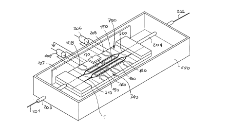
Fig. 22 shows a pers~ective view of a modulator device
according to the present invention, complete with
electrooptical structures, optical connecting fibers and
elect]ical connections, inserted inside its housing.
As shown in Figure 1, a Mach-Zehnder electrooptical
inter:Eerometric modulator device comprises:
- a portion 1 of crystalline substrate, for example made
of lithium niobate; this portion, corresponding to a
single device, consists of a unit obtained by means of
cutting of a substrate element and is referred to below
as "c]-Lip";
- an optical structure 100, comprising a first optical
waveguide section 101, which is then divided into two
branches 110, 120 located alongside one another and
joinirLg up again in a second optical waveguide section
102; the optical structure 100 is advantageously obtained
by means of diffusion on the crystalline substrate 1 of a
substance suitable f.or varying the refractive index
thereof and designed to allow an optical signal to pass
through;
- an electrode struct:ure which is arranged between the
two branches 110, 120 of the optical structure and which
comprises a polarization or bias electrode 150 and a
signal (or radiofrequency) electrode 160;
- a pair of ground e:lectrodes 130, 140 arranged outside
of the two branches 110, 120 of the optical structure;
the ,3ignal electrode 160 is connected to the ground
electrodes 130, 140 by a resistor termination 170.
In a preferred embodiment, the crystalline substrate is
made of lithium niobate (LiNbO3) which allows the
formation, on the surface, of monomodal waveguides with
CA 02230414 1998-02-2~
low losses, for examp]e using a technology which involves
the thermal diffusion of thin films of titanium, defined
by photolithographic techniques.
The optical waveguide section 101 is connected to a Y-
junction 103 which cornprises two diverging branches 103a,
103b connected to the branches 110, 120 located alongside
one another.
At the end of the branches 110, 120 located alongside one
another there is a second Y-junction 104, comprising two
converging branches :104a, 104b which join up and are
connected to the output waveguide 102.
Preferably the waveguides forming the portions 101, 102,
103, 104 described above are of the monomodal type.
The signal, bias and ground electrodes 110, 120, 150, 160
are arranged with respect to the waveguides of the
branches located alongside one another so as to produce
respective electric fields designed to modify, owing to
the electrooptical effect, the index of refraction of the
waveguides 110, 120; the arrangement described is such
that an electric field with the same potential is applied
along both the wavegu:ide branches 110, 120 of the optical
structure.
The electrooptical effect which is produced when
respective electrical signals are applied to the
elect.rodes consists in the variation in the index of
refraction of materia.l of the substrate subjected to an
elect.ric field.
Cryst:als without a center of inversion, such as for
CA 022304l4 l998-02-2
- 14 -
example lithium niobate mentioned above, are advantageous
for this purpose.
Other suitable materials are, for example, LiTaO3 or GaAs
or InP (semiconductor type); polymer (thermooptical)
materials, or materials of the silica-on-silica or
silica-on-silicon type, if necessary polarized, may also
be used.
In order to exploit the maximum electrooptical
coefficient, the force lines of the field applied should
be parallel to the optical axis z of the crystal; if the
crystal is cut along this same optical axis ("z-cut"
devices), the signal electrode 160 is advantageously
arranged on top of the waveguide with which it is to
interact; in devices cut along the optical axis x ("x-
cut"), in order to maximize the electrooptical
interaction with the optical structure, the signal
electrodes are advantageously arranged laterally with
respect to the optical waveguides with which they must
interact.
For manufacture of the modulators, cutting along the
optical axis x is preferred since z-cut crystals exhibit
marked pyroelectricity and thermal drift phenomena.
In the example shown in the Figure, the crystalline
substrate 100 is of the x-cut type.
The Mach-Zehnder modulator device, by means of
application of an electric field, allows variation in the
refractive index of two portions of the waveguide path,
causing a phase-shift between two fractions of an optical
signal which is propagated in said portions of the
CA 02230414 1998-02-2~
waveguide path in the crystal; this phase-shift is then
converted into a variation in amplitude of the signal, by
means of interference or evanescent wave coupling.
The injected optical signal which is propagated in the
initial waveguide section 101 is divided into two equal
parts at the first Y-junction 103; the two signal
fractions which are propagated in the waveguides 110, 120
then undergo equal and opposite phase modulation in the
central zone and interfere at the second Y-junction 104,
combining again in a first symmetrical mode with the
components in phase and in a second anti-symmetrical mode
with those in phase-opposition. The anti-symmetrical
mode is then irradiated in the substrate when the width
of the guide diminishes so as to allow propagation of
only the fundamental mode.
In a preferred embodiment the radiofrequency electrode
160 is located between the two branches 110, 120 of the
optical structure and the ground electrodes 130, 140 are
located outside the two branches, so as to create an
equal and opposite (push-pull) electrooptical effect on
the two guides, halving the drive voltage required.
The theoretical bases of operation of the Mach-Zehnder
modulators are described, for example, in "Waveguide
Electrooptic Modulators" by R.C. Alferness, IEEE
Transactions on Microwave Theory and Techniques, vol.
MTT-30, No. 8, August 1982, page 1121, already mentioned.
In a preferred embodiment, in addition to the modulating
signal electrode 160, an additional bias electrode 150 is
located on the modulator, having the function of
compensating for any optical path differences between the
~ CA 022304l4 l998-02-2
- 16 -
two branches 110, 120 of the interferometer, generated
during formation or due to external influences during
operation, such as for example mechanical and thermal
deformations. An electronic feedback circuit regulates
the voltage of this electrode in order to compensate for
any temporal or thermal drift and in general controls the
working conditions of the Mach-Zehnder device in
accordance with the requirements for use; an example of a
modulator of this kind is described in US 5,359,449.
A finished modulator, il:Lustrated in its entirety in
Figure 2, also comprises connecting fibers 201, 22,
applied by means of a pig-tailing operation and a support
structure, inside which the chip of the device is housed
and protected.
Said pig-tailing operation envisages the application of
respective fiber-carrying blocks 203, 204 inside which
the connecting fibers 201, 202 are housed.
The optical fibers for interconnection of the component
described are monomodal 8/125 type fibers, where 8
represents the diameter oE the core and 125 represents
the diameter of the cladding of the fiber, expressed in
~lm.
Preferably, the fiber used at the input 201 iS of the
bias-maintaining type, for maintaining the optical bias
state of the signali for this purpose it may be
advantageously provided with an elliptical core or
equivalent optical characteristics, for example the type
PANDA 8 /125 marketed by FUJIKURA.
The output fiber, for which bias maintenance is generally
CA 022304l4 l998-02-2
- 17 -
not required, may be for example the type SMF-FOS 8/125
produced by FOS Fibre Ottiche Sud S.p.A.
The device is then mounted in a housing consisting of a
metal support (not illustrated) which advantageously has
a ground plane 207 forming part of it and the electrical
connections of which are performed by soldering together
the radiofrequency signal electrode 160, terminated by
means of a resistor termination 170, and a signal
connector 205; the bias electrode 150 and a bias
connector 206; and the ground electrodes 130, 140 and the
ground plane 207, using a conductive adhesive or solder.
The longitudinal distances between the edges of the
device and the terminations of the electrodes strictly
determine the characteristics of the housing of the
device in the equipment for which it is intended and
these should conveniently satisfy predetermined
parameters.
For example, the ground plane 207 has holes 208, opposite
the terminations 150, 160, SO as to allow the fixing of
the connectors 205, 206 OIl the side 210 of the device in
contact with the ground plane 207.
During the pig-tailing process the position of the
electrical terminations poses limitations on the system
used for fixing the fibers since, during the process, it
is advantageous to apply a bias voltage to the modulator
in order to check the optical alignment thereof
(compensating for any non-ideal features of the structure
formed).
Figure 3 shows a crystalline substrate element 300, also
CA 022304l4 l998-02-2
- 18 -
called wafer, in which there are formed about 40 units 1
(from which the chips are obtained), each corresponding
to a device described above.
These chips typically have a length "I" of the order of
40 mm and width "w" of 2 mm and are formed in a wafer of
diameter "d" of about 3 inches (76.2 mm) and 0.04 inches
(about 1 mm) of thickness (size commercially available).
For example, a crystalline substrate made of lithium
niobate of about 76.2 mm diameter and 1 mm thickness, of
the "Optical Grade" type, is marketed by the company
Crystal Technologies or by others.
lS The size of the chips, and hence the total maximum number
of devices which can be made from a wafer, is subject to
limitations due, among other things, to the fragility of
the material, which would make a chip of width
significantly less than that indicated, prone to
breakages.
The length of the device, and hence that of the chip on
which it is formed, is dependent, moreover, upon the
formation of an effective electrooptical interaction;
typically, an effective length of interaction suitable
for the examples indicated is of the order of a few
millimeters, preferably of the order of at least ten or
so millimeters.
For formation of the device, making the most efficient
use of the wafer available, the minimum longitudinal and
transverse dimension of the chip required is therefore
defined and, on the basis thereof, the maximum number of
units possible on the surface of the wafer is designed.
' CA 02230414 1998-02-2~
-- 19
This design also takes account of the quantity of
material which is lost in the operations involving
cutting of the individual chips.
Figure 4 shows an alternative arrangement of the units in
the wafer 300, from which the chips are obtained,
comprising about 25 units having the same width "w" of 2
mm and length "I" of 50 mm, as required in the case where
a greater length of electrooptical interaction is
advantageous or it is desired to form several integrated
functions in the same device.
A technique for forming the devices described above from
a wafer of crystalline substrate is described with
reference to Figures 5 to 8 as regards the optical part
and 9 to 12 as regards the electrical part.
As shown schematically in Figure 5, the wafer 300 of
crystalline substrate is covered by a layer of
photosensitive material 410, referred to below as
"photoresist", which is sensitive to ultraviolet light,
as illustrated in Figure 5 and above it there is aligned
a mask 400.
The mask 400, for example made of quartz, is formed for
example by means of a photolithographic process
comprising the following steps:
- depositing a layer of photosensitive material
("photoresist") on a quartz sheet which has been covered
beforehand with chromium;
- selectively impressing the layer of photosensitive
material ("photoresist") by means of an electron beam
CA 022304l4 l998-02-2
- 20 -
which defines the design of the planned structures;
- removing the photosensitive layer from the zone where
impression has not occurred;
- chemically etching the layer of chromium left exposed;
- removing the residual photosensitive material.
The mask 400 thus formed, provided with the design for
definition of the optical waveguide structures for all
the chips to be obtained from the wafer, is superimposed
on and aligned with the wafer of crystalline substrate
300.
In the simplified diagram shown in the Figures, this mask
has a first plurality of zones 401, transparent with
respect to W rays, and a second plurality of zones 402,
opaque with respect to W rays.
This mask has moreover suitable reference points which
allow the impression, on the crystalline substrate, of
reference marks 610, shown in Figures 13, 16, for the
subsequent corresponding alignment of a mask for
definition of the electrical structures, described below.
The process used for definition of the guides using a
mask is of the photolithographic type.
The wafer of the crystalline substrate 300 lined with
photoresist and covered by the mask is subjected to
exposure to the ultraviolet: rays.
The zones of photoresist 410 not imprinted are then
chemically removed, by forming openings in the
photoresist at locations corresponding to the intended
waveguide paths.
CA 022304l4 l998-02-2
-- 21 -
As shown in Figure 6, deposition, by means of sputtering,
of a layer 430 of titanium over the entire surface is
then performed, and the remaining photoresist is then
eliminated (lifted off), together with the titanium
deposited on it, leaving the titanium 430 in the desired
positions only (Figure 7~.
Finally, as shown in Figure 8, the crystalline substrate
300 is placed in an oven, at a temperature of about
1030~C for 9 hours, so that the diffusion of the titanium
in the substrate forms the waveguides 440, modifying
locally the index of refraction of the crystalline
substrate 300 itself.
In the case where doped waveguides, for example
containing rare earths, are required, as a first step in
the process, deposition, over the entire crystalline
substrate, of a layer of rare earth (for example erbium)
followed by oven-diffusion (for example at 1100~C for 100
hours) may be performed.
Alternatively, the definition of an optical structure may
be obtained, for example, using a proton exchange
process, not shown in the figures.
This process comprises the steps of:
- covering the crystalline substrate with photoresist,
- aligning a mask having a design with portions which are
transparent and opaque with respect to ultraviolet rays,
on the crystalline substrate,
- exposing the crystalline substrate to ultraviolet rays,
- chemically removing the photoresist exposed to
ultraviolet rays,
CA 022304l4 l998-02-2
- 22 -
~ - immersing the crystalline substrate in a solution of
benzoic acid, and
- chemically removing the residual photoresist.
An example of a process performed for the formation of
the electrical structures is now described, with
reference to Figures 9 to 12.
With a process similar to that described above, a mask
500 is formed, said mask having a first plurality of
zones 501 transparent wit:h respect to W rays and a
second plurality of zones 502 opaque with respect to W
rays and designed to define the desired geometry of the
electrodes.
A thin layer 510 of titanium and a layer 520 of gold is
deposited on the crystalline substrate 300 on which the
optical waveguides have already been formed (only one is
shown in the figures); a layer of photosensitive material
410 iS then deposited.
Optionally, an insulating layer of silicon monoxide is
deposited over the entire surface of the crystalline
substrate, underneath the layers of titanium and gold, in
order to avoid excessive optical losses due to absorption
by the metal.
The mask 500 iS arranged on top of the crystalline
substrate 300, aligned with extreme precision (+ O. 25 ~m)
opposite the optical structure, by means of the reference
points 610 already mentioned; the whole assembly is then
exposed to the W rays through the mask, as shown in
Figure 9.
CA 022304l4 l998-02-2
- 23 -
Subsequently, the photosensitive material 410 not exposed
is chemically removed, :in a similar manner to that
described above and as illustrated in Figure 10, leaving
exposed the zones corresponding to the electrodes.
Then, as shown in Figure 11, galvanic growth of the
electrodes in a gold bath is performed, depositing a
layer of gold 530 in the zones where the photoresist has
been removed, until the desired thickness is reached.
Finally, by means of chemical etching, the residual
photoresist and the thin initial layer of titanium and
gold not grown galvanically is removed so as to obtain
the final structure schematically shown in Figure 12.
Following the operations described above, the crystalline
substrate 300 on which the optical and electrical
structures are present is cut along the points
corresponding to the individual units so as to form the
chips 1.
Cutting is performed, for example, by means of a circular
saw with a diamond-coated blade, driven by a numerical-
control machine, so as to ensure parallel alignment
between the cutting surfaces and the direction of the
optical guides. Prior to cutting, the crystalline
substrate is advantageously protected with a layer of
photoresist, so as to avoid damage to the surfaces.
The ends of the chips thu~; obtained are then subjected to
a lapping process, so as to obtain faces which are
perfectly flat and have the desired optical finishing
quality.
CA 022304l4 l998-02-2
- 24 -
During this step, several chips are bound together in a
bundle, alternating chips with complete optical and
electrical structures and plain unprocessed lithium
niobate blanks, using a low-melting wax. The bundle is
mounted on a support, able to exert a suitable pressure
between the surfaces to be smoothed and a rotating plate,
on which a solution comprising a granular adhesive is
applied in the form of droplets. As a result of the
subsequent smoothing operations, using granules with an
average diameter 3 and 0.1 ~m respectively, perfectly
flat surfaces may be obtained, whereby the quality of
said surfaces may be checked under a microscope by means
of interferometric measurements.
All the processing steps require a perfectly clean
environment and are preferably performed in "aseptic
chambers" with a controlled dust level.
In order to perform pig-tailing, two fiber-carrying
blocks 203, 204, in which the connecting fibers 201, 202
are housed, are arranged in the vicinity of the end
waveguides 101, 102 of the optical structure 100 of the
chip; an optical alignment check is then performed in
order to r,laximize the optical power transmitted and
reduce the insertion losses; a typical loss, for example
in the case of an analog modulator, is of the order of
3.5 dB. After checking the optimum alignment, the fiber-
carrying blocks 203, 204 and the optical fibers 201, 202
are fixed to the chip in the prechosen position by means
of a transparent adhesive.
The device provided with the optical connecting fibers is
then fixed onto a metal support and the ground electrodes
are connected, for example by means of a conductive
' CA 022304l4 l998-02-2
- 25 -
adhesive, to the ground plane 207; the electrical
connectors are soldered to the respective terminations of
the electrodes of the device and the radiofrequency
electrode 160 is connected by means of the resistive
termination 170 to the ground electrode. Finally the
entire assembly is housed inside a protective casing, not
illustrated.
The devices produced in accordance with that described
above are then subjected to a testing and analysis
procedure.
In order to verify the quality of the optical structures,
the transmission loss across two facing optical fibers at
the end of the device and an optical power measuring
device is measured; the typical loss for an analog
modulator is about 3. 5 dB.
In order to verify the quality of the electrodes, an
electric multimeter is used for measuring the resistance,
checking that the values measured coincide with the
predefined values, within the scope of a predefined
tolerance for example of the order of + 0.5 Ohm.
In order to qualify the performance characteristics of an
electrooptical modulator, the following parameters are
usually measured:
- modulation band, having as wide an amplitude as
possible in order to transmit a high number of basic
information elements (bits) per unit of time;
- insertion loss, measured in dB, which represents
attenuation of the optical signal over the entire device
(fiber-fiber) and which must be contained in order to
avoid the need for subsequent amplifications, capable of
CA 02230414 1998-02-2
- - 26 -
introducing excess noise;
- on/off voltage, which provides the voltage necessary
for passing from a constructive interference condition to
a destructive interference condition; and
- band ripple for a measurement of the irregularity in
the modulation amplitude.
Devices of the type described and illustrated above have
been manufactured by the Applicant with the following
methods.
During manufacture of the devices, the condition relating
to an arrangement of the electrodes which would allow
correct housing and interfacing of the device with the
external equipment, observing the predefined positions
for the optical and electrical connections, has been
observed.
EXAMPLE 1
With the process described above, several units were
formed on a wafer of subst:rate, as illustrated in Figure
13, each having several optical structures (three in
particular, denoted (in the figure) by lOOa, lOOb, lOOc;
corresponding alignment reference points 610a, 610b, 610c
are formed opposite these optical structures.
The optical structures of the units present on the wafer
are then examined under a microscope in order to select
from them the optical structures devoid of defects; then,
a common alignment position is prechosen, corresponding
to one of the three reference points 610, where there is
the least number of defects in all the units considered
(i.e. on the whole wafer).
CA 022304l4 l998-02-2
- 27 -
In this position, the arrangement of a mask 630 for the
formation of the electrical structures (the design of
which, for a single unit, is illustrated in Figure 14) is
determined; for this purpose the mask 630 has a locating
element 620 designed to be arranged in alignment with one
of the reference points 610 of the optical structures.
In this way complete unit:s are formed on the substrate
wafer, as illustrated schematically in Figure 15, from
which the chips are then obtained in order to form the
individual devices.
EX~iMPLE 2
Modulator devices of the type described have also been
produced with the following methods.
With the process described above, several units were
formed on a wafer of substrate, one of which is
illustrated in Figure 16, each provided with a pair of
optical structures 710, 720, each comprising two parallel
or substantially parallel branches 110, 120 and an
alignment reference point 610.
The optical structures '710, 720 are symmetrical with
respect to a rotation of 180~ about an axis perpendicular
to the surface of the unit, passing in an intermediate
position between the optical structures themselves.
A mask for forming the electrical structures of the
various units is then directly arranged on the optical
structures thus provided; the configuration of the mask,
for a single unit only, is illustrated in Figure 17,
CA 022304l4 l998-02-2
- 28 -
denoted by the reference number 730.
This mask has a design designed to form a pair of
electrical structures 740, 750, each comprising a ground
electrode 130, signal electrode 160 and bias electrode
150, which are symmetrical with respect to a rotation of
180~ about the same axis of symmetry of the optical
structures, and an alignment locating element 620
designed to be tallied with the reference point 610.
By means of this mask an electric structure has thus been
provided opposite to and in alignment with each of the
optical structures present on the individual units, as
illustrated in Figure 18.
Subsequently the wafer of crystalline substrate 300 was
then cut by separating the units so as to obtain the
desired chips and the faces of the devices obtained were
then smoothed; the optical characteristics of the
electrooptical structures formed by joining together of
the optical structures and the electrical structures
produced were then analyzed.
On the basis of this analysis, for each device, one of
the two pairs of electrooptical structures present on the
chip showing, upon said analysis, improved values
compared to a predetermined limit was chosen, and the
device was oriented so as to allow connection of the
preselected electrooptical structure to the electric
contacts 205, 206 and to the incoming and outgoing
optical fibers 201, 202 of the device in the housing
provided.
A modulator device formed in accordance with example 2 iS
- CA 022304l4 l998-02-2
- 29 -
shown in its entirety in Figure 22, in which the various
components are denoted by the same reference numbers
already used; the device is inserted inside a container
250, preferably made of metal, having openings through
which the electric contacts 205, 206 and the optical
connecting fibers 201, 202 emerge externally.
As can be seen from the Figure, one of the electrooptical
assemblies formed by a pair of electrical and optical
structures present on the chip is used and is connected
electrically and optically, whereas the other one remains
unused; on the basis of the assembly chosen, the
orientation of the chip is selected and in this way the
relative positions of the electrical connections and the
optical connections remain unaltered, independently of
the prechosen pair.
This thus allows assembly of the device in the equipment
for which it is intended, independently of the pair of
electrooptical structures selected.
The Applicant then assessed the rejects produced
following the two methods described: having called
n the number of devices per crystalline substrate
x the percentage of defective optical structures
y the percentage of defective electrical structures
a calculation was performed, from the binomial
distribution, of the probability of having m optical
rejects for a particular alignment between optical
structures and electrical structure:
m!(n-m)!X (I x)
CA 02230414 1998-02-2
- 30 -
and the total probability of having at least
one optical reject for an alignment:
p~O~ = ~ Pm
m =1
In the case of Example 1, in which three alignments are
possible, the probability of having an optical reject on
a crystalline substrate is defined by Ptot~ and hence the
percentage of optical rejects is PtOt3/n.
Adding to this value the defectiveness of the electrodes,
the percentage of optical/electrical rejects is:
P P
Stot = tot + y _ tot y
In the case of Example 2, there is rejection of a device
only if both the optical guides or both the electrical
structures or an optical structure and the opposite
electrical structure are defective; in analytical terms:
Stot = x + y + 2xy(1-x)(l-y).
From a numerical point of view, for x=y = 10~ and n=ll,
the percentage of rejects with the method described in
the first example is 12.9~, whereas with the method
described in the second example it is 3.6~.
Moreover, in contrast with the technique of Example 1,
operating in accordance with Example 2 results in
elimination of the step involving ex~m;n~tion under a
microscope of the optical structures for selection of the
set of optical structures present on the substrate which
has the least number of defects, thus making the method
more reliable and reducing the time necessary for
CA 022304l4 l998-02-2
- 31 -
carrying out thereof.
It is noted, moreover, that the formation of only two
optical structures on a single unit enables chips of
limited width to be formed, while maintaining a high
production output, without having to resort to the
formation of a considerable number of optical and
electrical structures on a single unit, from which the
configuration with the least defects is chosen.
The symmetrical arrangement of the optical structures and
the electrodes on the units described in Example 2 is
preferable, in order to maintain the same relative
arrangement for both the possible configurations of the
device which may be selected during the final test prior
to the formation of the electrical and optical
connections, thus allowing the assembly of the device in
the equipment for which it is intended independently of
the prechosen pair of electrical and optical structures.
In the case where this condition is not critical, for
example for equipment which involves the connection of
the electrodes by means of wires (wire bonding), the
length and arrangement of which is not rigidly defined,
the requirement for symmetry may be dispensed with.
Figure 19 illustrates the arrangement of the electrical
structures 910, 920 and the optical structures 930, 940,
according to the invention, in a different device, in
particular a phase modulator; for this device also, a
substantial reduction in rejects is obtained forming the
optical structures and electrical structures, without
intermediate checks, and selecting for each device the
correct pair during final checking.
CA 02230414 l998-02-2
- 32 -
Figure 20, moreover, shows the integrated structure of an
amplitude modulator and a phase modulator, combined in
the same chip and formed by means of the process
according to the invention; in this figure the various
components present have been indicated with the same
reference numbers used before.
Figure 21 shows an example of equipment in which the
integrated optical device manufactured in accordance with
the invention may be used.
The figure shows a wavelength converter, designed in
particular for conversion of a modulated optical signal
800 supplied at the input, having a wavelength ~1, into a
modulated optical signal 809 with a wavelength i~2,
emitted at the output.
The equipment comprises a receiving photodiode 802, which
receives the optical signal 800 and converts it into a
modulated electrical signal, which is sent by the
electronic amplifier 803, where it is amplified, and from
which it is supplied to the radiofrequency signal
connector 806 of an electrooptical modulator 805,
2 5 suitably constructed according to the invention.
The modulator 805 performs the consequent optical
modulation of the continuous light signal 807 with a
wavelength ~2 received from the laser source 804, and
emits a modulated optical signal 809. Part of the
modulated optical signal 809 with a wavelength ~2
provided by the modulator via a directional coupler 810
is sent to the control circuit 808, which is connected to
the connector 811 for biasing the modulator 805 and
CA 02230414 1998-02-2
- 33 -
performs stabilization of the operating point of the
modulator 805 itself.
By way of conclusion, the production of devices according
to Example 2 allows a reduction in the processing time
for a wafer owing to elimination of ex~m-n~tion, under a
microscopic, of the optical guides and an in increase in
the efficiency of the process with a reduction in the
cost and the production time, without involving any
modification during the manufacturing and assembly
process.
The embodiments described may be subject to variations,
modifications and replacements by the person skilled in
the art, which fall within the scope and spirit of the
invention, such as for example the formation of other
electrooptical devices comprising on a single substrate
additional optical and electrical structures interacting
with one another, such as, for example, filters or
lasers.