Note: Descriptions are shown in the official language in which they were submitted.
-
CA 02230529 1998-02-26
PCT/U~ 96/1408&
u~ 1996
~ .
DIGITALLY P~OGRAMMAB~E MULTIFUNCTION
RADIO SYSTEM ARC~I~ECTURE
C~OSS REFERENCE TO RELATED APPLICATIONS
This application is related to currently filed
U.S. Applica~ions entitle~ Co~mon Transmit ~odule For
A Programmable Di.gital ~adio, having U.S. Serial No.
and Westinghou~e doc~et number 58,S50;
and Co~mon Receive Kodule For A Digital Programm~ble
Radio System, h~ving U.S. Serial No.
and Westinghouse docket number 58,56~, both
incorp~rated by re~erence herein.
BACKG~OUND OF T~E Ihv~N~ ON
Field of the Invention
~ he pressnt invention i~ directed to a radio that
can include a receiver and pos~ibly a transmitter and
that can be digitally reconfigured to operate over a
broa~ radio band and with di~erent ~ignal formats,
and, more particularly, to an architecture of a sys~em
that provides dynamically programmable and
configurable channels with maior portions o~ digLtal
and analog ch~n~el components ccmbin~d at t~e signal
frequency translation and waveform processing stages
2Q to simpli~y recon~iguration rlexibility and to be
scalable t~ many different types o~ integrate~ radio
system applications.
~escription of th.e Related Art
At one extreme conventional ~ nication~
CA 02230~29 1998 - 02 - 26 PCT/U~ 9 6 1 1 4 0 8 8
~IIJS ; ~ r~ E~ 1996
,
navigation and identification (CNI) multi-radio suites
are comprised of an independent and different type
radio channel for each radio functional thread. At
the other extreme, integrated programmable radio
systems cross-couple various elements of multiple
channels, which results in a highly complex system of
tightly coupled resources. Both approaches, including
hybrids of the two approaches, have advantages as well
as major disadvantages. For example, the independent
channel systems must have complete backup systems for
all critical systems, such as instrument landing
systems. This is very costly. The cross-couple~d
systems are extremely difficult to maintain because
fault isolation is difficult. These cross-coupled
systems are also difficult to control. Maintaining
secure channel isolation is also a problem.
Many commercial and military applications require
multiple communication, navigation, identification
(CNI), or telemetry radio frequency (RF) functions as
well as other types of RF signal functions to be
performed at a single location, ~or example, air
vehicles, ships, space platforms, ground-mobile
vehicles and personnel, fixed stations, communication
hubs of various types, etc. all require multiple radio
functions at a single location. Thus, there is a need
for a better partitioning of radio system elements
that allow the use and reuse of identical common
programmable components or modules to significantly
reduce the cost and eliminate other disadvantages of
prior art implementations.
SUMMARY OF THE INVENTION
It is an object of the present invention to
provide a programmable multifunction radio with an
architecture that allows maximum flexibility at
minimum cost.
CA 02230~29 1998-02-26
9 6 / 1 4 0 8 8
'.~ 1996
, .
It is another object of the present invention to
provide a radio that can be quickly reconfigured for
many different types of radio functions.
It is an additional object of the present
invention to provide a radio which will operate over
a frequency range of approximately 2 MHZ to 2000 MHZ.
It is also an object of the present invention to
provide a system that can ope~rate in frequency ranges
outside of the preferred range using simple block
frequency converters in interface units.
It is a further ob]ect of the present invention
to provide common identical modules that can be easily
reconfigured allowing reduction in the number of
spares or backup modules required for a given level of
system availability.
It is still another object of the present
invention to provide a receive radio channel that is
assigned to and programmed for a basic functional
thread for a particular radio function from a wide
variety of radio functions; and where the receive
radio channel can be quickly (i.e., dynamically)
reprogrammed for different radio functions.
It is an object of the present invention to
provide a receive radio channel from RF input to a
digital (usually serial) bit stream output that is
normally comprised of an RF interface unit, usually an
antenna interface unit, that contains hardware that is
specific to one or relatively few radio functions, and
a common receive module tha~t can be programmed for
many different types of radio functions, and where
most of the radio channel functionality is contained
in the common receive module; and where the receive
radio channel can also be comprised of channelized
message processing (CMP) modules, information security
3~ (INFOSEC) modules and/or applique processing modules
CA 02230~29 1998-02-26 p~T~U~ 9~ / ~ 408 8
iUS U ~ LJ~ 1g96
.
as defined below.
It is a further object of the present invention
to provide the definition of a programmable (i.e.,
common) receive module that accepts different types of
radio signals over a very wide radio frequency range
(e.g., the approximate 2 MHZ to 2000 MHZ frequency
range), performs the necessary frequency translation,
analog-to-digital conversion and digital processing,
including demodulation of waveforms of various
combinations of amplitude, frequency and phase
modulation, and outputs a digital bit stream of
information of that is usually serial and qf
relatively low speed in order to simplify physical
interconnections and reduce the complexity of physical
interconnections among system modules.
It is also an object of the present invention to
provide the definition of a common receive module
having analog circuitry (e.g., frequency translation
circuitry) and high speed digital circuitry in the
same small unit such that the relatively noisy digital
circuits do not corrupt the sensitive analog circuits.
It is an additional object of the present
invention to provide the definition of an integrated
radio architecture with suitable isolation such that
2S the relatively noisy digital circuits do not corrupt
the sensitive analog circuits.
It is another object of the present invention to
provide a radio architecture where a common receive
module can be switched among different interface units
(usually antenna interface units) each dedicated to
one or relatively few radio functions in order to
provide receive radio channels for many different
radio functions.
It is a further object of the present invention
to provide a transmit radio channel that IS assigned
CA 02230~29 1998-02-26
9 ~ / 1 4 0 8 8
3 3EC l996
, . .
to and programmed for a basic functional thread for a
particular radio function; where the transmit radio
channel can be dynamically reprogrammed for different
radio functions.
It is an object of the present invention to
provide a transmit radio channel from a digital
(usually serial) bit stream input to RF output that is
normally comprised of a common transmit module that
can be programmed for many different types of radio
functions and an interface unit, usually an antenna
interface unit, that contains hardware that is
specific to one or relatively few radio functions, and
where most of the radio channel functionality is
contained in the common transmit module; where the
transmit radio channel can also be comprised of
channelized message processing (CMP) modules,
information security (INFOSEC) modules and/or applique
processing modules as defined below.
It is a further object of the present invention
to provide the definition of a programmable (i.e.,
common) transmit module that accepts a digital
(usually relatively low speed serial) bit stream of
information, performs the necessary digital processing
including carrier modulation of various combinations
of amplitude, frequency and phase modulation
waveforms, digital-to-analog conversion and frequency
translation, and transmits different types of radio
signals over a very wide radio frequency range (e.g.,
the approximate 2 MHZ to 2000 MHZ frequency range).
It is another object of the present invention to
provide the definition Of a programinable transmit
module having analog circuitry (e.g., frequency
translation circuitry) and high speed digital
circuitry in the same small unit such that the
~relatively noisy digital circuitS do not corrupt the
CA 02230~29 1998-02-26
P~ 9 ~ 1 1 4 0 8 &
. ~ . . . , , ~. ~ 1 9
sensitive analog circuits.
It is also an object of the present invention to
provide a radio architecture where a common transmit
module can be switched among different interface units
(e.g., usually antenna interface units) each usually
dedicated to one or relatively few radio functions in
order to provide transmit radio channels for many
different radio functions.
It is an object of the present invention to
provide the definition of a programmable transmit
module having analog circuitry (e.g., frequency
translation circuitry) and high speed digital
circuitry in the same small unit such that the
relatively noisy digital circuits do not corrupt the
sensitive analog circuits.
It is also an object of the present invention to
provide the definition of external analog, signal and
power interfaces to antenna interface units such that
the relatively noisy digital circuits in the rest of
the system do not corrupt the sensitive analog
circuits in the antenna interface unit.
It is an object of the present invention to
provide a control interface to a antenna interface
unit such that any noisy digital signals associated
with the control such as high-speed clocks for data
synchronization is turned off during RF signal
reception and transmission.
It is still another object of the present
invention to optimally divide or partition the
functions of a radio to reduce the size and cost of
the modules.
- It is also an object of the present invention to
provide a radio system in which the modules can be
easily replaced.
It is an object to provide a system in which the
.
CA 02230~29 1998-02-26 ~ .rJ{J;3 9b ~ 14 Q 8
/US O 3 DEC 1991~
~ .
channels can be dynamically reprogrammed.
It is a still further object of the present
invention to provide a programmable radio architecture
whereby programmable receive and transmit modules can
be quickly reprogrammed for different radio functions.
It is an object of the present invention to
provide a programmable radio architecture whereby
programmable receive and transmit modules can be
quickly reprogrammed from internally stored
application programs.
It is a still further object of the present
invention to provide a programmable radio architecture
whereby programmable receive and transmit modules can
be quickly reprogrammed by downloading from externally
stored application programs via a suitable bus.
It is an object of the present invention to
provide a radio architecture where certain types of
reconfiguration or control of channel resources
including the associated antenna interface unit module
and common receive or transmit module (frequency
channel select, antenna select, BIT initiation, etc.)
can take place by downloading from external memory or
can be manually loaded (e.g., from a keyboard or
display menu) via a suitable system bus the parameter
data necessary to perform the limited reconfiguration
or control.
It is a further object of the present invention
to provide a universal backup receiver module and a
universal backup transmit module capable of performing
many of the functions within the radio frequency band
of interest.
It is an object of the present invention to
provide modules that can be programmed for future
waveforms.
. I~ is another object Of the present invention to
CA 02230~29 1998-02-26
PC~ 9 6 1 1 4 ~
tJ.~,~ O ~ aEC 1996
provide modules in which hardware and software
upgrades can be made at the module level rather than
-impacting the hardware of two or more modules or the
whole system.
It is also an object of the present invention to
provide modules that can be easily specified for an
open architecture.
It is another object of the present invention to
provide a system in which there are fewer programmable
module types than prior art programmable systems.
It is an object of the present invention to
provide modules that are arranged in such a way (i.e.~
a dedicated hardware channel per radio function(s) in
use) that permits a simple radio control architecture
compared to prior art programmable systems.
It is an object of the present invention to
- provide a radio architecture where channelized message
processing (CMP) modules associated with the common
receive and transmit module channels can, if needed,
perform additional message processing on the digital
(usually relatively low speed serial) bit stream
signal connections to the common receive and transmit
module.
It is also an additional object of the present
invention to provide a radio architecture where
information security (INFOSEC) modules, sometimes
combined in the same module with channelized message
processing, can be inserted in receive and transmit
channels to perform information security and simplify
security isolation in integrated programmable radio
systems.
It is a further object of the present invention
to provide a radio architecture where information
security (INFOSEC) modules, can be combined in the
same module with channelized message processing.
CA 02230~29 1998-02-26 p ~ 9 ~ / 1 4 0 ~ 8
~t~S a 3 [~EC 1996
.
It is an object of the present invention to
provide a radio architecture where applique modules
associated with the common receive and transmit
modules can, if needed, be added in modular fashion to
perform additional high speed signal processing beyond
the capability of the common receive and transmit
modules.
It is also an object of the present invention to
provide a controller to manage the multiple module
assets of an integrated radio system, and to provide
an interface with other equipments.
It is also an additional object of the present
invention to provide a control architecture where the
highest speed processing is self-contained within the
separate programmable common receive or transmit
modules, and, if employed the separate CMP, INFOSEC
and applique modules.
It is an object of the present invention to
provide a simplified control architecture where
control of the RF processing resources in a radio
channel, including the common receive or transmit
module in the channel and the antenna interface unit
module associated with the channel comes from the
programmable common receive or transmit modules in the
radio channel.
It is a further object of the present invention
to provide a programmable radio architecture where
spare receive or transmit channels can be dynamically
programmed to replace failed receive or transmit
channels.
It is an additional object of the present
invention to provide a programmable radio architecture
where receive or transmit channels already assigned to
a radio function or functions can be dynamically
programmed to replace failed receive or transmit
~v~ ' : - ~3
. CA 02230~29 1998-02-26
,.J~,,~,~'i,,/~ 9~I 14~8 8
- -, 7 ~ US O 9 DE~ 1996
channels of a higher priority.
It is an object of the present invention to
provide a programmable radio architecture where
receive or transmit channels, the modules associated
with the channels, and modules or other functionality
of the overall radio architecture such as the radio
controller or module interconnections can be easily
monitored for faults and in the event of such faults
the system can be automatically reconfigured to
correct the fault by reprogramming spare or lower
priority modules, assigning nonprogrammable spare
modules, or assigning spare interconnections.
It is another object of the present invention to
provide programmable common receive and transmit
modules with programmable external interfaces that can
be used for a variety of interface applications,
including for both control functions and for signal
flow, where such interfaces may be serial or parallel,
synchronous or asynchronous, unidirectional or
bidirectional, to include both standard or custom
protocols; where such external interfaces may utilize
transceivers, receivers or transmitters (i.e.,
drivers) for differential (i.e., dual rail)
connectivity in order to reduce noise pickup.
It is an additional object of the present
invention to provide an architecture where the CMP
modules, INFOSEC modules and applique modules can be
easily inserted into the modular architecture,
regardless whether such modules are programmable for
different CMP, INFOSEC and applique functions or
whether such modules incorporate off-the-shelf
hardware are specific to one or several of these
functions.
It is an object of the present invention to
provide a radio architecture where applique modules
CA 02230~29 1998-02-26
PC~ 9~ / 14 0 8 8
3tUS O 9 ~EC 1996
11
associated with the common receive and transmit
modules can, if needed, perform additional high speed
signal processing beyond the capability of the common
receive and transmit modules.
It is another object of the present invention to
provide modules arranged so that simplified BIT/FIT is
possible.
It is also an object of the present invention to
provide modules that are arranged in a way that
permits relatively easy maintenance and checkout.
It is a further object of the present invention
to provide a system in which the modules haye
simplified external interfaces.
It is an object of the present invention to
provide the modules that permit simplified interfaces
between modules.
It is an object of the present invention to
provide a radio architecture with flexible
interconnections between the various system units and
external equipments that can be used for a variety of
interface applications, where such interfaces may be
serial or parallel, synchronous or asynchronous,
unidirectional or bidirectional, to include both
standard or custom protocols; where such interfaces
include, for example: message busses and control/data
busses that are used to pass raw data information and
control signals between the programmable common
receive or transmit modules (or, if used, channelized
message processing modules, INFOSEC modules and~or
applique modules), the system controller and various
external equipments; an antenna interface unit ~AIU)
contrbl bus between the programmable common receive
module and the AIU to control the receive assets in
the AIU associated with the same channel as the
programmable receive module: a transmit bus plus
CA 02230~29 1998-02-26
96/ 1408 8
0 9 DEC 1996
various discretes to control the transmit assets in
the AIU associated with the same channel as the
programmable transmit module; a transpond bus between
associated receive and transmit modules for
transponder or repeater applications, or to share
processing hardware; an applique bus to an associated
applique module to perform additional signal
processing beyond the capability of the digital
processing portions of the receive or transmit
modules; and busses to other external elements or
modules as provided by the flexible programmable
interfaces of the programmable receive, transmit,
channelized message processing, or INFOSEC module.
It is also an object of the present invention to
provide the modules arranged to make changes in system
capacity for different applications easy by adding or
deleting modules.
It is another object of the present invention to
provide modules arranged in a way that simplifies the
certification process for a new radio function.
It is a still further object of the present
invention to provide modules that permit less analog
(i.e., RF, IF or video) switching between modules.
The above objects can be accomplished by a radio
system architecture that partitions or divides the
functions of a radio into channels and divides the
functions of each channel into two major functions: l)
antenna interface dedicated to certain radio
functions, and 2) mixing, (i.e., frequency translation
or conversion) and signal processing to/from a
digital bit stream that can be programmed for many
different types of radio functions, and may further
partition the mixing through signal processing
functions into -the functions of: a) programmable
analog mixing and b) programmable .digital signal
CA 02230~29 1998-02-26 p C ~/~ S 9 6 / 14 0 8 8
~/US O 9 DEC 199~
. .
processing. Control and user interface functions
needed for a particular application are also
functionally partitioned. A typical received RF
signal pathway will encounter an antenna, an antenna
interface module that contains several receiver front
end elements dedicated to certain radio functions and
a receiver module that can be programmed for many
different radio functions. The receiver module may be
further partitioned into an analog submodule that
performs frequency translation to produce analog
common intermediate frequency signals and a digital
submodule that converts the analog intermediate
frequency signals into a digital signal, further
frequency translates the intermediate frequency
signal, demodulates the signal and performs the other
signal processing necessary to provide a useful
relatively low speed digital information signal
version of the information signal of the received RF
signal. A typical transmitter pathway includes a
transmit module partitioned into a digital submodule
that performs digital signal processing and modulation
of a relatively low speed digital information signal
to be transmitted into a common intermediate frequency
signal which is converted into an analog intermediate
frequency signal, and an analog submodule that
performs analog frequency translation, followed by a
power amplification and interface module that contains
several transmit elements dedicated to one or more
specific radio functions and an antenna. Digital
control and user interface modules can also be
provided along with modules that perform additional
channelized message processing functions, modules that
perform information security functions on the low
speed digital information signal, or in rare cases,
which perform higher-speed signal processing directly
CA 02230~29 1998-02-26
9 ~a ~ 1 4 0 8 8
~OIUS O 9 DEC l996
14
on the radio waveform. Various combinations and
quantities of the above modules can be used to satisfy
many different types of multifunction radio
applications.
These together with other objects and advantages
which will be subsequently apparent, reside in the
details of construction and operation as more fully
hereinafter described and claimed, reference being had
to the accompanying drawings forming a part hereof,
wherein like numerals refer to like parts throughout.
BRIEF DESCRIPTION OF THE DRAWINGS
Figure 1 illustrates the components of a simple
receiver system 100 according to the present
invention;
Figure 2 illustrates the components of a simple
transmitter system 200 according to the present
nvention;
Figure 3 illustrates a more complex transmitter
and receiver system 300;
Figure 4 illustrates the functional processing
that can be performed in a system such as illustrated
in figure 3;
Figure 5 depicts the details of an antenna
interface and power amplification module (AIU) 104/308
in more detail and where not all of the illustrated
elements are needed for every communication,
navigation and identification (CNI) channel;
Figures 6A and 6B depict the components of a
receiver module 106 in more detail;
Figures 7A and 7B depict the components of a
transmit module 204 in more detail;
Figure 8 illustrates a communication system using
the architecture of the present invention in a
commercial airplane communication suite;
Figure 9 illustrates an example of bus
CA 02230~29 1998-02-26
96 / 14 0 ~ 8
P~ C 1996
. .
partitioning;
Figures 10 and 11 depict levels of redundancy
providable by the present invention;
Figure 12 illustrates a single channel multi--
function communication receiver;
Figure 13 depicts a multifunction navigation
receiver using a single channel;
Figure 14 shows. a multifunction communication
transceiver using a single channel;
Figure 15 depicts a multifunction navigation
transceiver;
Figure 16 illustrates a radi~o
repeater/transponder with or without the option of
information security (INFOSEC);
Figure 17 illustrates an identification
transponder providing antenna diversity with the
option o f security;
Figure 18 depicts a multiple receive channel
transceiver system;
2 0 Figure 19 depicts a single channel radio system
requiring additional message processing;
Figure 20 illustrates a two channel transceiver
with the option of security and additional message
process ing;
Figure 21 depicts a multiband transceiver using
multiple modules;
Figure 22 depicts a multiband transceiver using
multiple modules with information security modules
added;
Figure 23 illustrates a military airplane
integrated CNI system;
Figure 24 depicts a multiple channel transceiver
system with user-dedicated security modules;
Figure 25 illustrates bus connections for common
3 5 receive and transmit modules;
.~ ~c~
CA 02230~29 1998-02-26
9 ~ ¦ 1 4 (~
~e~ 3~ E ~ 1996
~ .
16
Figure 26 shows bus connections when a
channelized message processing (CMP) module is
connected to a common receive module;
Figure 27 shows bus connections when channelized
message processing modules are each connected to a
common receive module and a common transmit module;
Figure 28 shows bus connections when a single
channelized message processing module is connected to
both a common receive module and a common transmit
module;
Figure 29 shows bus connections when an
information security (INFOSEC) module is connected t,o
a common receive module;
Figure 30 shows bus connections when an
in~ormation security modules are each connected to a
common receive module and a common transmit module;
Figure 31 shows bus connections when a single
information security module is connected to both a
common receive module and a common transmit module;
Figure 32 shows bus connections when an
individual red (i.e., high domain) CMP module, black
(i.e., low domain) CMP module and INFOSEC module are
all connected in the same channel as a common receive
and/or transmit module.
Figure 33 illustrates bus connections when red
CMP, black CMP module and INFOSEC functionality are
all contained in the same module are connected in the
same channel as a common receive and/or transmit
module.
Figure 34 depicts separate antenna interface
units for receive and transmit paths associated with
the same (full- duplex) radi~ function.
Figure 35 shows how an applique processing module
is connected to a common receive or common transmit
module.
t
CA 02230~29 1998-02-26
~TII~I~ 96/14~8
J~ ~ ~ L~G l~9~
~ .
17
Figure 36 depicts a single common receive module
being shared among separate antenna interface units.
Figure 37 illustrates an AIU that is functionally
specific to several radio functions.
Figure 38 illustrates an AIU for a muiti-function
antenna.
DESCRIPTION OF THE PREFERRED EMBODIMENTS
Although the discussion of the present invention
usually refers to CNI radio functions and
applications, the programmable nature of the invention
enables the invention to be applied to RF signals
modulated with any combination of amplitude, phase
and/or frequency modulation that can be programmed by
the programmable RF channel modules (i.e., the common
receive module and the common transmit module)
discussed later. Such RF signals not only include CNI
radio functions but, for example, radio signals
associated with radar, electronic warfare (for example
electronic surveillance, electronic countermeasures,
electronic intelligence), telemetry or positioning.
Furthermore, the ability of the RF interface unit
(usually referred to as the antenna interface unit
also described later) to perform frequency conversion
permits the programmable RF channel modules to service
electromagnetic wave signals of potentially any
frequency.
A radio channel is a single physical path for
transmitting electrical signals from a single source
(e.g., a microphone input to a distant transmitter) to
a single destination (e.g., a speaker output from a
local receiver). A receive radio channel includes all
the hardware and software required to accept the
incoming RF signal and convert it to a form suitable
for human or equipment interface. A transmit radio
channel is the converse of the receive channel and
CA 02230~29 1998-02-26
'.~,"'~.J~_'. 96/14~88
O 9 D~C lgg~
?
~ .
18
sometimes a receiver and transmitter operating on the
same frequency are together referred to as a
"channel". At some point in the receive channel the
signal is reduced (i.e., demodulated and perhaps
decoded, decrypted, etc.) to the basic information
that is to be received (analog ~r digitized voice or
data).
An end-to-end (i.e., distant transmitter to local
receiver) channel contains only a single radio channel
at any given time, although a large portion, but not
the entire portion, of the hardware in an end-to-end
channel can service multiple channels at the same
time. An example of the latter is where a distant
transmitter takes a single carrier and, with different
portions of a hardware channel, frequency multiplexes
multiple frequency channels, each with a different
source, so that all pass through the rest of the
transmitter's bandwidth, through antennas, through
space to receive antennas, through most of the
receiver until finally different hardware portions
demultiplex the separate channels onto separate lines
for different human or equipment end users. The
transmitter;s frequency multiplexing, for example,
either separates the different channels into different
frequency bands that are usually contiguous, or the
multiplexing is "direct sequence" where all the
channels overlap the same frequency region with
orthogonal codes. In this way all the channels can be
simultaneous, but either way, separate hardware is
eventually needed to multiplex and demultiplex each
channel. Even if all the multiple simultaneous
channels are buffered and operated on one at a time
with the same hardware a different hardware buffer
would be needed for each channel. Thus, each
end-to-end hardware channel contains only one source
.
CA 02230~29 1998-02-26
~cr~ 96/ 1408 ~
3/US ~ 9 ~EC 1996
t
,
19
and one destination.
The one-to-one relationship of a single
end-to-end hardware link versus a single channel is
more complicated when time multiplexing (TMUX) is
included. All the same end-to-end hardware for
multiple channels could be used if non-simultaneous
channels are allowed, such as when each channel has a
separate time slot on the same "line," which includes
the airwaves. For TMUX systems separate hardware for
multiple channels is not needed. For example, a
single radio could be used and tuned to different
channels, one at a time. But no matter how it is
done, separate hardware is still needed, or at least
an allocated portion of hardware, to access a
different channel. For example, even a single coil
that is tuned to different frequencies needs a
"longer" tuning rod for more channels. Similarly, a
digital radio that is programmed for different
channels at different times needs a portion of
circuitry allocated to the different parameters and
characteristics of each channel such as operating
frequency., Of course, if more than one channel is
needed simultaneously, separate speakers, etc. would
be needed. Thus, regardless of the implementation, it
appears a separate end-to-end hardware channel is
needed for each source-to-destination link.
Previously it was noted that a large portion of
an end-to-end hardware channel plus minimal additional
hardware (e.g., buffers, correlators, demodulators)
can service multiple channels at the same time. In
the case of the present invention where one of the
"hardware channels" comprised of a single common
receive or transmit module can service multiple
channels provided the channels fit within the designed
bandwidth. This is accomplished by configuring small
-
CA 02230~29 1998-02-26
PCT/~ 96/140~ -
9 DEC1996
but different portions of digital circuitry in a
transmit or receive module to multiplex or demultiplex
information for different channels. For example,
multiple contiguous frequency channels (i.e., slots),
as well as multiple direct-sequence coded channels,
can be received and demodulated provided the total
bandwidth of multiple channels fits within receive
module's bandwidth.
A receive (or transmit) radio channel is defined
as one in which one or more modules in the channel are
connected in series and are dedicated or programmed to
pass a particular type of signal or information. ~A
hardwired module (or simply "module") is defined as
one in which all the elements are dedicated to passing
a particular signal or type of information, and for
which none of the elements are ever used (e.g.,
switched) in series with elements in another channel
to process a particular signal or flow of information.
An example of two separate channels each
comprised of a single module is two separate AM/FM
table radios, which can be of the same type or of
different types. Each radio can be tuned to receive
any number of radio channels (i.e., radio stations),
one at a time. However, during normal operation none
of the circuitry in one radio is used in conjunction
with some of the circuitry in the other radio. Each
radio consists of a "hardwired" module, that is, all
circuit elements are contained in a box and none of
these elements are routinely used in con~junction with
the elements in another box. Note that circuit
elements can be switched inside the box for different
radio frequency channels or for different radio
waveforms like AM versus FM. But, as noted, the
circuit elements are not shared between modules.
3~ These types o~ radios are "federated".
~ 3~L~
CA 02230~29 1998-02-26
~ PC~ S 96/1408 8
- ~/US O 9 ~E~ 1996
The benefits of having everything federated in
one radio box is that once the radio is built and
tested, there are no additional problems uncovered
when different circuits in one channel are connected
to work with circuits in another channel. Everything
is controlled in one box.
These AM/FM radios are programmable -- not so
much because they can be tuned to different channels
but because they can be "programmed" for different
waveforms, i.e., AM and FM, even if this "programming"
only involves throwing a switch that switches between
internal AM and FM circuits.
The digitally programmable radio system
architecture of the present invention allows for a
much wider variety of waveforms over a much wider
frequency range than AM and FM radios. To do so the
invention does not attempt to place all the necessary
channel functionality for a wide variety of radio
functions into one oversized module because the module
would be extremely large and costly. This oversized
module would not be size and cost effective for radio
channels in system applications that needed only the
functionality for a subset of radio functions,
including system applications which require many
multiple simultaneous radio channels of arbitrary
radio functions from a wide library. Instead, the
digitally programmable radio system architecture
optimally partitions radio channels into antenna
interface unit (AIU) modules, each of which are
usually dedicated to specific radio functions and
which comprise a relatively small portion of a
channel's functionality, and into a receive (or
transmit) module that is programmable to receive (or
transmit) a wide variety of radio functions and which
comprises a relatively large portion of the channel
CA 02230529 1998-02-26
PC~illS 96/14088
-~f~ 9 DE~ l9g6
, .
22
functionality for these radio functions. Furthermore,
these programmable, or common, receive and transmit
modules have a minimal amount of unused hardware when
servicing any particular radio function. During
operation, and depending upon the radio function being
serviced, common receive or transmit modules are
connected to different radio functionally-specific AIU
modules, each of which are tailored for particular
radio function(s) and for particular system
applications. Multiple simultaneous receive or
transmit channels are obtained by providing multiple
common receive or transmit modules (although, in som~e
cases, multiple simultaneous radio channels can be
serviced by a single common receive or transmit module
as explained later). Also, the common receive and
transmit modules can be quickly reprogrammed, via
either internal program memory or by downloading
programs (including modified or new programs) from
external memory.
Thus, in the architecture of the present
invention an AIU plus a common receive or transmit
module does not have a totally hardwired channel
because common receive or transmit modules can work in
series with different AIUs, and because, for
redundancy, a single AIU can work with different
(primary or spare) common receive or transmit modules,
sometimes simultaneously for hot redundancy. The
present invention has optimally partitioned a radio
channel into hardwired modules to gain the benefits
that such partitioning affords. The p resent
invention partitions the architecture so that a
considerable amount of circuity is contained in one
box and never shared with circuity in another box.
This affords the benefits of having most of the common
~stuff in one box that can be built the same way for
~ c~3i~
CA 02230~29 1998-02-26
9 6 / 1 4 0 8 8
3~/US O ~ D ~C 1996
23
every communication, navigation and identification
(CNI) radio function in every channel and built the
same way for many different system applications.
There are fewer module types for the bulk of the
channel functionality for a wide variety of CNI radio
functions and other types of RF signal functions
compared to the prior art federated approach that uses
many different types of modules for the same number of
CNI radio functions.
In contrast to federated radios, cross-channel
radios share circuits among channels, i.e., some of
the elements are used (e.g., switched) in series with
elements in another channel to process a particular
signal or information. The digitally programmable
radio system architecture also has cross-channel
capability type features. In the present invention
the partitioning of the cross-channelization is
important.
At the extreme of cross-channelization, one could
partition the circuitry in a channel such that every
basic element (resistors, capacitors, transistors,
etc.) is separate, and put in switches between each of
these elements such that any of them can be used in
combination any of the other basic elements to perform
a wide variety of electrical functions, some of them
simultaneously. Obviously the switching networks
would be horrendous and would be much larger than the
elements themselves. Performance would also be poor
because of electrical isolation, confliats between
resources (i.e., circuit elements) needed, difficulty
in testing every combination and isolating faults in
the event of a failure, etc.
On the other hand, the "cross-channel" approach
of the present invention limits the number of separate
modules in a channel to an AIU plus hardwired common
CA 02230~29 1998-02-26 ~ 9 6 / 1 4 ~ 8
9 ~EG l~
.. . .
. .
24
receive and transmit modules where the interfaces to
the common receive and transmit module units is only
RF and a low-speed serial bit stream. Most of the
channel functionality is contained in these hardwired
common receive and transmit modules. The present
invention provides for additional processing on
relatively low serial bit streams with additional
modules (channelized message processor - CMP or
information security processor - INFOSEC) that, for
the most part, are hardwired in the same channel and
are not shared with other channels unless reasons of
redundancy (or INFOSEC control) make it appropriate to
do so. The invention architecture is flexible enough
to accommodate this latter type of sharing if desired.
Another way of saying that channels are
partitioned is that they are optimally connected,
i.e., a channel comprised of an AIU plus a receive or
transmit module, each with only an RF/serial data
interface for the information) that can be programmed
to service a wide variety of CNI functions, and
additional CMP modules that are usually connected only
to the common receive or transmit modules they support
unless the benefits of cross-switching the CMP modules
proves beneficial from a system standpoint.
An important feature of the present invention is
not only that the architecture is channelized but that
the hardware is also partitioned into hardwired
modules. All architectures, including federated and
cross-channel, have hardware strings or "channels"
that are hardwired (for the federated) or
switch/allocated (for the cross-channel) to a
particular CNI function. But in the case of the
present invention the hardware channels are
partitioned as explained later, where most of the
radio functionality in a channel is contained inside
CA 02230~29 1998-02-26
5 6 / ~ 4 0 8 8
u ~ ~EC 1996
one of two modules which form the heart of a hardware
channel: Either a common receive module or a common
transmit module.
The prior art federated architecture dedicates a
single box (sometimes with the option of a remote
control unit and perhaps a separate power amplifier)
to one (or a few) CNI functional channels. The box
contains most or all of the elements that the present
invention places in separate AIUs that are dedicated
to each CNI function or group of functions. But the
federated channel is not programmable for a wide range
of CNI functions.
None of these federated schemes utilize a
relatively large block of common circuitry that
services and performs a wide range of functionality
(frequency conversion, analog-to-digital or
digital-to-analog, modulation/demodulation, etc.) for
different radio functions. Federated boxes require a
considerable amount of hardware overhead to account
for multiple radio functions, which makes these boxes
relatively large and costly, albeit some of these
federated boxes try to reduce overall size and cost
for one particular application by making it possible
to manually plug in different submodules to service
different CNI functions or modes. But this plug-in
approach precludes the availability of multiple radio
functions by simply reprogramming the units. The
interfaces of these submodules are not simple.
Furthermore, unlike the digitally programmable radio
system of the present invention, the boxes only
service a limited number of communication, navigation
or identification functions, but not a wide variety of
all three types of functions.
A cross-channel architecture is designed to
service more than one or a few CNI radio functions.
CA 02230529 1998-02-26
t~ ~ 3~ ~ 96 / 140 8
9 ~ ~ ~ 19 96
26
Prior-art programmable cross-channel architectures
consist of many different type modules, each of which
contain less channel functionality than the common
transmit or receive modules of the present invention.
This approach requires considerable RF switching and
high-speed parallel bus switching, both of which are
undesirable, in order to eventually dedicate a string
of modules to a particular CNI function. Because the
modules at each point of the string, e.g., frequency
translation, receiver preprocessing, are comprised of
different module types depending on the CNI functions
to which the string is programmed, there is minimal
commonalty between channels. That is, each channel
can be programmed for only one or a few types of CNI
functions. Also, much of the digital processing is
partitioned in relatively large processors that
service multiple CNI functions at the same time, thus
making channel isolation (e.g., for security purposes)
and resource allocation/control of the entire string
a virtual nightmare. Prior art cross-channel
architectures are difficult to scale to different size
multifunction radio applications.
on the other hand, the architecture of the
present invention is channelized with partitioning of
the functions of the radio into several module types,
AIU and common receive module (for a receive channel)
and two module types (AIU and transmit module) for a
transmit channel (albeit the AIU for the receive
channel is almost always combined with the AIU for the
transmit channel to form a single AIU).
The receive module is "common" in the sense that
it can accept RF and be programmed, either by analog
switching or digital software or both, to perform
frequency translation and signal processing down to a
low-speed serial blt stream in a channel that is
. ,,, _ , . . 3 ~s~ t
CA 02230~29 1998-02-26 '
3 96 1 1 4~ 8 8
t~/V~ ~ 9 DEC 1996
27
programmed to one of a wide variety of CNI functions.
Conversely, the transmit module is "common" in the
sense that it can accept a low-speed serial bit stream
and be programmed to perform signal modulation and
frequency translation to RF for wide variety of CNI
functions. It is also desirable that the common
modules can be rapidly programmed for different
communicatio~, navigation and identification (CNI)
functions by loading a new program.
The partitioning of the radio channels in the
architecture of the present invention includes as
follows: (1) all the functionally-specific hardwa~e
that drives up hardware overhead in a commo~ receive
module or a common transmit module is contained in the
AIU, which, incidentally, contains relatively few
functional elements compared to the rest of the
channel, that is, the bulk of the radio channel
processing is performed in the common modules and a
small part in CNI functionally-specific AIUs; and (2)
the signal path of the common receive or transmit
modules requires only a single RF ccnnection to the
AIU, and only relatively low-speed, usually serial
interfaces between the modules and the rest of the
system. The latter (2) avoids undesirable analog
switching between modules of different types,
eliminates parallel high-speed busses, reduces
isolation problems between channels that share the
same processor, and avoids the other disadvantages of
the cross-channel approach previously noted.
In the partitioned architecture of the present
invention, message processing over and above what can
be performed in a common receive or common transmit
module can be performed in additional modules, namely
channelized message processing (CMP) or information
secur~ty (INFOSEC) modules, that are allocated to the
CA 0223os29 l998~02~26 P~T/us 9 6 / 1 4 0 8 8
' - 7 ' '' ~ U~ a 9 D~C ~996
28
same channel. But these additional modules need only
operate on relatively low speed, usually serial data.
In particular, adding INFOSEC modules in this manner
simplifies security isolation in integrated
programmable radio systems. Also, in the rare cases
that may be needed for some system applications,
applique modules can be connected to common receive
and transmit modules via relatively short parallel
busses of moderate speed to perform additional high
speed signal processing beyond the capability of the
common receive and transmit modules.
The present invention, by properly partitioning
the various elements in each radio channel and
providing appropriate signal isolation and filtering,
provides a minimal size, weight and cost solution for
a communication, navigation and identification (CNI)
multi-function radio suite. It can be tailored in a
modular fashion to many types of applications. It
also affords all the advantages and essentially none
of the disadvantages of the above "individual" and
programmable "cross-channel" approaches previously
mentioned. Moreover, the architecture uniquely scales
to single-channel radio applications where the single
channel can be programmed for any subgroup of CNI
functions selected from a much wider library than
prior art programmable radios.
See Table A for some of the possible radio
function applications of the invention architecture.
Table A: CNI and Telemetry Radio Functions
Communication Identification
HF Clear Voice/Data ATCRBS/IFF Transpond
HF AJ IFF Interrogate
HF Link ll ~ode S
-
CA 02230~29 1998-02-26
~T/~S 96/1408 8
VHF AM TCAS
VHF AM Encrypted
VHF FM Navigation
VHF Encrypted omega Nav*
SINCGARS Loran-C*
VHF ACARS ILS Localizer
UHF Clear ILS Glideslope
~ UHF Encrypted ILS Marker Beacon
Havequick Versions VHF Omni-Range (VOR)
Military UHF SATCOM PLRS/EPLRS
Airphone Tactical Air Nav System
(TACAN)
JTIDS Distance Measuring Equipment
(DME)
Commercial SATCOM Precision DME
RAM Mobile Data Global Positioning System
Cellular GLONASS (Soviet GPS)
Citizens Band Radar Altimeter*
PCS Microwave Landing System
(MLS)*
Commercial TV
VHF Data Radio (VDR)
Industrial, Medical and Scientific (IMS)*
Telemetry
ACMI: Air Combat Maneuvering Instrumentation
*Indicates that a block converter is used in the
antenna interface unit to convert the radio signal to
the input range of analog submodule 104. Other RF
functions too numerous to mention can also be
accommodated using a block converter.
ACARS: Aircraft Communication Addressing and Reporting
System
CA 02230~29 1998-02-26 ~ 9 6 / 1 4 O 8 8
~OIUS ~3 9 DEC 1996
ATCRBS: Air Traffic Control Radar Beacon System
EPLRS: Enhanced Position Location Reporting System
IFF: Interrogate Friend-or-Foe
ILS: Instrument Landing System
JTIDS: Joint Tactical Information Distribution System
PCS: Personal communication system
SINCGARS: Single-Channel Ground-to-Air Radio
TCAS: Traffic Collision Avoidance System
The architecture's optimal partitioning of
channels allows easy fault isolation, module
replacement and module backup as well as allowing
security isolation to be easier to provide. The
architecture also utilizes a special partitioning of
radio elements of a channel in integrated CNI radio
system applications, along with guidelines for bus
interconnections between the elements, that makes
practical the use of identical programmable
common-module channels with minimal hardware overhead.
Each channel is partitioned functionally by dividing
signal capture or radiation, receive signal
preconditioning and/or transmit power amplification,
r a d i a t i on , fr e qu e n c y c o nv e r s io n,
modulation/demodulation, additional signal processing,
security processing and special message processing
into different modules.
Hardware that is common among many different
types of CNI radio functions and many different types
of multi-function radio system applications is placed
inside common programmable modules. High-overhead
hardware (i.e., hardware that is specific to only a
single or relatively few CNI functions, or specific to
a particular application, that is, non-common
components) is housed separately outside the common
programmable modules. So doing reduces common-module
_
CA 02230~29 1998-02-26
9 6 / 1 4 0 8 8
;c~ ';f ~ ~ L. E ~ 1996
31
overhead to the point where the size of the common
RF/IF and digital processing hardware is small enough
to place in a single plug-in housing of reasonably
small size. All the high-speed processing and
parallel interconnects are completely contained inside
the common module housings, thereby greatly reducing
backplane complexity, EMI and crosstalk.
Although the goal is to make various modules as
common as possible among different CNI radio functions
and different integrated CNI radio system
applications, it may be beneficial to "tailor" a
common module such that it is common among different
CNI functions in a particular system application but
the module is functionally different among
applications. An example is where receive and
transmit common module circuitry to handle wideband
CNI functions is not included in the receive and
transmit common modules for an application that only
requires narrowband CNI functions. (In this case the
original common modules have been "depopulated.")
Note, however, that the latter modules can still be
common among different narrowband CNI functions in the
same application. Another important example is where
some applications require bus isolation circuitry to
be contained internal to the various modules to
protect the bus from module failure. Because such
circuitry is relatively bulky, especially when there
are many bus I/0 connections, it may not be desirable
to contain the isolation circuitry in modules not
requiring it. Also, because modules are programmable
to handle multiple CNI functions, the internal
isolation circuity may not be necessary as discussed
later with respect to bus interface units.
The present invention provides common modules
(receive and/or transmit) that are programmable to
'~
CA 02230~29 1998-02-26
f~ 9 6 / 14 0 8 8
lUS O 9 ~EC 1996
operate over a range of approximately 2 MHZ to 2 GHz.
If the disclosed architectural partitioning is
not employed, the programmable common modules would
carry excessive size and cost overhead, and such
overhead would preclude their utility in practical
applications.
Within this description the major radio elements
that are partitioned are indicated as modules or
submodules. Elements enclosed by dotted or dashed
lines are not necessarily required for all
applications. The indicated modular partitioning
(with the minor exception discussed later) eliminates
the need for relatively high speed (greater than
several MHZ) parallel bus interconnections between
modules. The partitioning also characterizes an open
architecture of a particular type, where the interface
requirements of each module are defined such that
modules can be developed, upgraded and procured from
competitive suppliers. Module and bus configurations
for various type example applications are discussed
later herein.
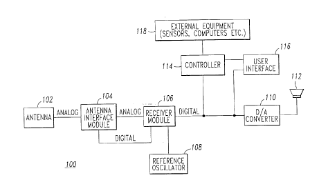
A channelized receiver system lO0 which is
programmably dedicated to a single channel, according
to the present invention, is illustrated in figure 1.
The system includes an antenna 102 that can be as
simple as an AM antenna or as complex as a
multifunction (or multielement) antenna such as one
that services some or all the L-band commercial or
military communication navigatian and identification
(CNI) functions. The antenna 102 is coupled to an
antenna interface unit, (AIU) module 104 that includes
all the control, amplification, filtering and other
receiver front-end circuitry necessary to interface
with the particular antenna 102 being used, and which
provides the analog output signal from the antenna 102
CA 02230~29 1998-02-26 ~ 9 6 / 1 4 0 8 8
~tO/~lS O 9 DEC 1996
~ .
33
to a common receive module 106 in a state that permits
the subsequent common receiver module to process the
signal of interest commensurate with performance
requirements. Depending upon the actual AIU
implementation, the AIU module 104 can have a
capability for performing changes in received signal
level, received interference levels, transmit/receive
connectivity and signal connectivity to/from various
common receive or transmit modules under the control
of a common receive module 106. The common receive
module 106 performs the analog functions of converting
the received baseband signal into an intermediate
frequency signal using a reference oscillator signal
from reference oscillator 108, converts the
intermediate frequency analog signal into a digital
signal, performs any further down-converting,
demodulation and special signal processing in the
digital domain and provides a digital information
signal, as a low speed digital signal, preferably on
the order of one megabit per second, suitable for
subsequent interface to various equipment including
equipment operated by a human user. For example, if
the antenna'signal is a navigation signal the system
would output demodulated and decoded navigation
signals while if the signal is an AM broadcast radio
signal the output would be a digital version of the
sound produced by an AM radio. The digital output of
the receiver module 106, if necessary, would be
converted into a useable form. In the navigation
example, a positioning display may be produced. In
the case of an AM radio output, a digital-to-analog
converter in an audio interface 110 converts the
digital signal to an analog sound signal which is
converted into sound by a conventional speaker 112 or
amplifier speaker system if necessary. When the
.
CA 02230~29 1998-02-26
9 6 / 1 4 0 8 8
9 ~c 1996
34
receiver is a fixed frequency channel system, such as
is required for a radio repeater, the programmable
characteristics of the common receiver module 106 can
be programmed through ROM, dip switches, jumpers, etc.
albeit the common receive module is preferably
software programmable via controller 114. The system
100 can include a controller 114, which can be as
simple as a digital channel sçlector unit, such as
when module 106 is used in a simple application such
as changing frequencies in an AM radio, or as
complicated as a workstation computer when multiple
CNI programs are to be downloaded and controlled among
multiple channels. The system 100 can also have a
user interface 116 coupled to the controller 114 and
the receiver module 106. Like the controller 114,
this interface can be as simple as a digital channel
selector or a complicated as a workstation computer.
In the case of the AM radio the interface would
include a channel selector. The controller 114 and/or
receive module 106 can also be connected to other
external equipment 118 examples of which will be
described later. The common receive module 106 will
be discussed in more detail later with respect to
figures 6A and 6B.
A channelized transmitter system 200, as
illustrated in figure 2, includes some of the same
type components as the receiver system 100. A signal
source 202 provides an information signal for the
transmitter system to transmit. The signal can be a
digital signal, such as would be received from the
receiver side of a repeater, or could be an analog
signal as shown in figure 2. -If digital it can be
input directly into a common transmit model 204 and,
if analog, the information signal is converted by an
analog-to-digital converter in the analog interface
~ w ~ ~ ~ ~ . ~ ~ ~ J
CA 02230~29 1998-02-26
9 6 / 1 4 0 8 8
O~LiS O 9 ~EG ~99~
206 into a low speed digital signal. The transmitter
module 206, like the receiver module 106 can be
controlled by ROM, dip switch, etc. programming in
those situations where the characteristics of the
channel are fixed, such as a repeater radio, or can be
programmably controlled by a controller 206, which can
be the same controller 114 as shown in figure 1, under
the control of the user interface 208, which can be
the same user interface 116 as is in figure 1, in
other situations. The controller 206 as well as the
other modules that appear in both figures 1 and 2 can
be shared between the receive and transmit sides i~n
situations where appropriate, such as a two-way
(transceiver type) radio systems found in air traffic
control systems and military communications. These
modules that are shared between receive and transmit
paths may perform the same functions for each path,
e.g., reference oscillator or channel control, or they
may perform different functions. For example, the
antenna interface unit module 104 may perform antenna
switching and filtering for both receive and transmit
paths; but the AIU may perform tunable filtering,
receiver protection, automatic gain control, etc., for
the receive path, but perform separate transmit
filtering to remove unwanted signal emissions and
perform signal power amplification 'o raise the power
of the transmitted signal to the desired level before
the RF signal is provided to the antenna 100. It is
also possible to share some of the AIU functionality
among different CNI functions, for example, the same
power amplifier in AIU 104 can be used to transmit
various radio functions in the same band such as IFF,
Mode S, ATCRBS, TACAN and DME by sharing the same
channel among these radio functions on either a
simultaneous or time-multiplexed basis. The common
~/ ~ ~ J . d ~; ~ ~ t~ G ~~ _ S 3
CA 02230~29 1998-02-26
~ ; 9~/ 1408 8
. ~' lJ 9 'JL~ 1996
36
transmit module 204 will be discussed in more detail
later with respect to figures 7A and 7B.
Figure 3 illustrates a combined channelized
transmitter/receiver system 300 suitable for
communication, navigation and identification (CNI)
applications. Only a single channel is shown but it
applies to any CNI application and can be replicated
to form parallel channels. In this more complex
embodiment, the same programmable common transmit 204
and receive 106 modules as found in the less complex
systems of figures 1 and 2 are used, but have the
programmable characteristics suitable for the more
complex application set accordingly. In these more
complex applications the controller becomes the more
complex controller/data processor module 302, the
simple interface is replaced by a bus system 322 that
allows multiple channels to be addressed and
controlled. System bus 322 can be segregated into
physically separate buses as dictated by bus traffic
considerations and/or formats and protocol
requirements of the various system elements including
external units. The bus interface unit (BIU) 304 may
be employed between various system elements in systems
requiring special hardware for electrical connection
considerations such as isolation and line voltages,
and where it is impractical to place such hardware in
a common receive or transmit module. The BIU
functionality could be housed in a separate module or
could be contained in a backplane or wiring harness
assembly that connects the various modules. In
certain applications a RF switching module 306 is
necessarily added to the antenna interface module 308,
thus changing the particular components of the module
308. The channel can also be provided with special
signal processing modules 310, a channelized message
CA 02230~29 1998-02-26
9 6 / 1 4 U 8 8
; 0 9 DEC 1996
processing (CMP) module 312, information security
modules 314, 318, and 320 necessary for secure
communications, and, when secure channelized message
processing is required, a channelized message
processing module 316 on the secure side of the
information security (INFOSEC) module 314. When
signals requiring a very rapid response time are
received, such as the pulse position demodulation and
pulse position reply within one microsecond required
in identify friend or foe (IFF) communications, a
transpond bus 321, which can be either a serial bus or
parallel bus of moderate speed, can be used to provide
the input pulse position to the transmitter module 204
where the pulse position reply is produced and
transmitted. This output/input between the receiver
106 transmitter 204 is in addition to the system bus
322 that is provided for configuration control,
input/output of information signals, etc. Transpond
bus 321 can also be used for radio repeater
applications as well as to share digital processing
hardware among the receive module 106 and the common
transmit module 204.
Figure 4 depicts the range of functions that can
be provided by a single dynamically programmable
transceiver channel, such as the channel system 300
illustrated in figure 3, which is coupled to different
types of antennas, for example the three different
type of antennas 330, 332, and 334. The operations
and processing noted in figure 4 are not meant to be
all inclusive for all radio functions of interest, nor
are all the processes indicated utilized for every
radio function. However, as can be seen the modules
are capable of performing all of the functions
necessary for a radio within the ap~roximately 2MHZ to
2GHz RF band of interest. Furthermore-, some functions
CA 02230~29 1998-02-26
P~IUS96/14~88
9 aEC l996
, .
38
(e.g., error correction,) may be performed in one of
the other modules other than the one indicated. For
some applications, certain elements, e.g., the CNI
controller/data processor 302, can be further
partitioned into multiple elements but preferably as
long as such partitioning is not at a high-speed
parallel bus interface. However, neither the common
programmable receive module 106 nor the common
programmable transmit module 204 should be further
partitioned into separate boxes, although as will be
discussed in more detail later the common modules 106
and 204, each preferably contained within a single
rack mountable, preferably plug-in unit, are divided
into analog and digital submodules that are shielded
and isolated, with respect to EMI, from each other.
These common receive 106 and transmit 204 modules are
partitioned to contain all the RF/IF conversion
circuitry in the channel, and to have only relatively
low speed serial busses at their I/O interfaces.
Conversely, elements such as the channelized message
processors (C~lPs) 312 and 316 and information security
(INFOSEC) elements 314, 318 and 320 (and even the
common programmable receive module 106 and common
programmable transmit module 204) can be combined into
fewer modulesO However, such combining of modules may
increase module size and cost overhead if the larger
module is to be used in multiple places (i.e.,
channels or applications) because not all elements o~
the module are necessarily used in each place.
As can be seen from the above discussion the
programmable digital radio (PDR) architecture of the
present invention uses two common module types: a
programmable common receive module 106 and a
programmable common transmit module 204 which form the
heart of ~he system. The two modules can serve as
CA 02230~29 1998-02-26
96/14088
~iU~ a 9 ~c ~996
39
primary modules dedicated to a single channel function
or reprogrammable for different primary RF functions
or serve as universal backup modules capable of
performing any of the functions required of a primary
module. The modules 106 and 204 are called "common"
because the same module can be programmed to process
one of many different types of CNI radio functions and
such processing can be rapidly time-multiplexed among
multiple CNI radio functions. Thus, a single radio
channel, such as system channels 100, 200 and 300, can
be programmed for a particular CNI function (or for
time-multiplexed CNI radio functions of different
types) and two or more radio channels can each be
programmed for the same or different radio functions
that must operate in exactly the same time period. It
is also possible for the hardware normally assigned to
a single channel to service multiple channels that
are, for example, contiguous in frequency and/or
formed by code division multiplexing the same RF
carrier. Moreover, these common receive 106 and
transmit 204 modules can also be used in different
integrated CNI radio applications on different
platforms. Although not mandatory for some
applications, but included as part of the
architecture, as explained later, the channelized
message processors (CMP) and information security
(INFOSEC) modules can also be common programmable
modules. Furthermore, these three modules can also be
combined into a single common programmable INFOSEC/CMP
module as illustrated in figure 4. Quite often the
CMP modules 312 and 316 would be combined with the
INFOSEC module 314 because many CNI functional
channels requiring the INFOSEC module 314 also require
the CMP modules 312 and 316, and the consolidation of
these modules can reduce overall hardware by utilizing
CA 02230~29 1998-02-26
9 ~ 1 ~ 4 0 8 8
Ol~S ~) 9 ~EC 1996
, .
components common to the combined functionality.
When in the receive mode (see figures 3 and 4),
a received RF signal for each CNI function is routed
from one or more antennas through the antenna
interface unit (AIU) 308 into the common programmable
receive module 106. The common receive module 106
uses analog RF/IF and digital signal processing to
perform .the necessary frequency translation,
demodulation and bit stream formatting to a signal
carrying the desired information to be conveyed (and
sometimes referred to herein as the digital
information signal) such that, except for the rare
case described later, where additional high-speed
processing (such as LPI processing) is required
directly on the waveform prior to demodulation, the
output of the common receive module 106 is normally
relatively low speed, serial data comprising a digital
information signal appropriate to various application
terminals such as audio equipment, displays,
instruments, etc. The need for high-speed parallel
bus interfaces between modules is ~or the most part
eliminated.
In many cases, the receive module 106 performs
all necessary signal processing and modem functions
such that the data output from the receive module,
under the control of the controller 302, is passed to
a terminal 336, such as an audio interface or a
man-machine interface (MMI). An analog radio
frequency-(RF) carrier modulated signal, for example,
a carrier modulated with an analog voice signal, that
is received by the common receive module 106 is output
as, for example, a digital voice signal and is passed
to, for example, a voice terminal in the MMI 336 where
it is converted back to analog audio and sent to
speakers or headsets. The path to the terminal can be
CA 02230~29 l998-02-26
P~T/I~ ~6 /1408
AalU~ ~ 9 aEc 1996
41
either a bus that services multiple CNI channels and
terminals, or it can be a dedicated path from a
particular channel, such as channel 324, to a
particular type terminal, such as a printer or a FAX
machine. If necessary, the conventional bus interface
unit (BIU) 304 is inserted in the path, either for
reasons of conversion to a standard bus protocol, or
for electrical compatibility (line drivers, voltage
transformation, isolation, etc.) when such
compatibility is not included within the common
modules 106 and 204.
In other cases the data output from the receive
module 106 is first passed through the controIler 302,
which manages the integrated radio assets including
system busses such as 322 and 324 and, in some
applications, performs a data processing function. It
can also act as a gateway to other application busses,
such as bus 336. It is also possible to further
segregate the controller, data processor and gateway
functions into separate modules.
For special cases, when the receive module 106 is
unable to handle all the message processing associated
with the channel, a channelized message processor
(CMP) module 312 is assigned to the receive module
106. When an INFOSEC module is present a CMP module
316 to handle the secure message processing is
inserted on the secure (i.e., red) side of the INFOSEC
module 314. The CMP is analogous to an expansion
board including a special purpose high speed digital
processor. However, relatively low speed serial data
is passed from the receive module 106 to the CMP 312.
It is anticipated that as digital processing hardware
becomes smaller and less expensive, more CMP-type
processing can be per~ormed within the common receive
mQdule 106 with acceptable size and cost overhead. At
CA 02230~29 l998-02-26
! ~ J ~ 9 ~ 8
- - A~U~ O 9 DEC 1996
42
that point some CMP modules will not be necessary.
CMP functions can also be performed in the INFOSEC
modules as discussed below.
In the rare instance where relatively high-speed
multi-bit processing must be performed on the received
waveform before demodulation, such as
low-probability-of-intercept (LPI) type processing, it
may be necessary to perform such processing in a
separate special processing or applique module 310.
Although the applique module 310 typically takes the
place of the signal processing elements within digital
submodule 600 (see figure 6B to be discussed in more
detail later), and normally operates directly on the
narrowband or wideband A/D converter output 622 of
switch 606, it is not connected directly to 606
because the physical commonality of the receive module
106 including digital portion 600 should not be
changed. Essentially the output of the narrowband ADC
604 or the wideband ADC 602 is routed through 606, 608
and 614 to the applique bus 330. The applique module
310 WiIl normally operate directly on the ADC 602 or
604 output although some intervening processing via
the other digital elements, such as 608, 610, 611, 612
and even 614 is possible. Such processing external to
the receive module 106 requires multi-bit lines, i.e.,
parallel interconnects which may be referred to as
applique busses, between the receive module 106 and
the applique module 310. However, the specialized
applique module 310 preferably resides adjacent to the
receive module 106 being serviced, so the
electromagnetic interference (EMI) associated with
moderate speed multi-bit lines is confined in a
relatively small volume and is minimized.
In the relatively fewer instances of receiving a
signal requiring additional signal processing
J ;~",~ u ~ ~ ~t
CA 02230~29 1998-02-26
i~ 9 6 / 1 4 0 8 ~3
G 9 ~ 1996
.
43
capability (for example, LPI/LPD processing) that is
not economical to place in every common receive
module, and where such additional processing is of a
type that is not economical to place in a CMP module,
such additional processing can be placed in an
applique module. In this case, with reference to
figure 35, the output from the ADC in the common
receive module 3502 and prior to demodulation of a
digital intermediate frequency signal is routed,
perhaps with intervening processing in the common
receive module that does not add unacceptable latency
in the receive signal path, to the applique bus 3504
and then to the applique module 3506 for the
additional (e.g., LPI/LPD) processing. After applique
processing, the signal can either be routed back to
the common receive module 3502 via applique bus 3508
for additional processing (again without unacceptable
signal latency) before passing the signal to black
control data bus 3510 (or perhaps a separate black
message bus 3512) and then, as the digital information
signal to CMP module 3514. Or, after applique
processing, the signal can be routed directly via the
applique module 3506 to the black control/data bus
3510 (perhaps via a separate black message bus 3512)
as the digital information signal to CMP module 3514.
If CMP and/or INFOSEC are not employed, the output
from applique module 3506 via the control/data bus
3510 (or perhaps a separate message bus 3512) would
pass as the digital information signal directly to the
system controller 3516 and/or external user terminals
3518 via control/data bus 3520 or multiple access
message bus 3522, both of which busses would then be
black. The particular signal routing paths are
determined by the module interconnection layout (e.g.,
the backplane connectivity) for the particular system
CA 02230~29 1998-02-26 ~ 9 6 / ~ 4 0 8 8
19 ~ 6
, .
44
application. Because the data rate for applique
processing is relatively high, applique busses are
parallel and of higher speeds than the serial digital
information signal.
On the other hand, for some applications it may
be desirable to use a special-purpose receive module
to eliminate the need for extra I/O pins on the common
receive module 106, and to eliminate the
moderate-speed extra-bit lines in the backplane. This
special-purpose receive module may be somewhat larger
than a common receive module 106 (in pitch but not in
footprint) to contain the applique ~unctions.
However, even this special-purpose receive module
would possess the analog and digital circuits that are
found within the common receive module 106. As the
size and cost of digital processing continues to
decrease, it should be practical to house the
additional processing within common transmit 204 and
receive 106 modules with acceptable size and cost
overhead such that it is economically and physically
acceptable to utilize this module that includes the
applique functions for CNI functions that do not
require the applique.
Whenever required, information security (INFOSEC)
modules, such as 314, 318 and 320, provide COMSEC
(communication security) on a channelized basis, which
often involves the description of classified messages.
That is, the output of a receive module 106 is fed
into an INFOSEC module 314 (see figure 3) before being
combined with other data and passed to the PDR
controller and/or various terminals. In addition, the
INFOSEC modules can provide TRANSEC (transmission
security) on a channelized basis, which often involves
control (such as a channel frequency hopping sequence~
of assets residing in the common receive and transmit
CA 02230~29 1998-02-26 P ~ ~IU S 9 ~ / 1 4 0 8 ~
O/US O 9 ~E~ 1~96
~ .
modules 106 and 204. In such cases the key for the
control, such as the decoding code for COMSEC or the
hop sequence for TRANSEC, is received in classified
form from the INFOSEC load device 320, is routed to
the INFOSEC module 314 associated with the desired
channel, is unwrapped (i.e., declassified) in either
the INFOSEC management module or the INFOSEC module,
and is passed to the receive and transmit modules in
the same CNI channel via a bus interface (either the
normal CNI control data bus or a separate TRANSEC
bus). For applications that require INFOSEC modules,
it may be desirable to place the CMP processing (i.e.,
the relatively low-speed message processing that
cannot be handled by the common receive module) into
the INFOSEC module. The INFOSEC/CMP combination, as
shown in figure 4, is particularly attractive when the
additional message processing associated with a
particular radio channel is of both the unclassified
(black) and classified (red) variety.
Associated with the INFOSEC capability is an
INFOSEC management module 318 and provisions for key
loading via a load panel 320. The key INFOSEC point
with regard to the architecture is that it is
performed on a channelized basis, which not only
simplifies the INFOSEC implementation but also
simplifies the isolation of INFOSEC functions among
channels of different security levels. Furthermore,
channelized INFOSEC simplifies the certification of
the entire system when channels are added or modified.
The details of how the channelized system architecture
handles a mix of clear and classified information in
an integrated radio suite are provided later with
respect to figure 22. Also, the advantages and
disadvantages of associating INFOSEC modules with each
channel as opposed to each application device (as
CA 02230~29 1998-02-26
~; r f ~ ~3 9 ~ / 1 4 0 8 8
$~ 3 9 DEC 1996
46
shown in figure 24) Will be discussed later.
The transmit path is similar to the reverse of
the receive path, where data and digitized voice
originate at various sources, and are passed under the
5 control of the controller 302 (see figure 3) to the
common programmable transmit module 204 (through
INFOSEC and CMP functions if required by the
application). The transmit module 204 contains both
digital and analog IF/RF circuits. It normally inputs
relatively low speed serial data, performs digital
modulation and associated processing, such as
interpolation and waveform generation, to produce a
common intermediate frequency signal, performs
digital-to-analog conversion, frequency translates the
signal to the appropriate CNI band, and passes the
baseband analog signal to the AIU 308 where it is
power amplified. The signal is then routed to the
appropriate antenna for free space transmission.
Similar to the common receive module 106 ~ the
20 integrated common RF/digital transmit module 204
eliminates the need for high-speed parallel bus
interfaces between modules.
Also, similar to a common programmable receive
module 106, CMP and INFOSEC modules can be utilized to
25 complement a common programmable transmit module 204~
Usually a single CMP and/or INFOSEC module would
service both the transmit 204 and receive 106 modules
associated with a half-duplex CNI channel. Separate
receive and transmit CMP and INFOSEC modules could be
utilized for full-duplex CNI operation, or the
full-duplex operation could be embedded in single CMP
module and INFOSEC modules.
As in the receiver the applique module 310 would
replace the processor 704 (see figure 7A to be
discussed in more~detail later) and communicate over
~w~ ~ ~3
CA 02230~29 1998-02-26
9 6 / 1 4 0 8 8
U ~ o~c 199~
the bus 330 through 702 and 708 directly to the DAC
710, although in some applications additional
processing might be performed by some of the elements
in digital submodule 700.
Similar to applique processing in a receive
channel, and with reference to figure 35, when
transmitting a signal requiring signal processing of
relatively high rate and beyond the capability of a
common transmit module (for example, LPI/LPD
processing), the digital information signal output
from CMP module 3514 via black control/data bus 3510
(or perhaps a separate message bus 3512) is routed,
prior to digital carrier modulation, to applique
module 3506 for the additional (e.g., LPI/LPD)
processing, and then via applique bus 3508 to the
digital-to-analog converter in common transmit module
3503, perhaps with intervening processing of
sufficiently low latency in common transmit module
3503. Alternately, the signal output from CMP module
3514 via black control/data bus 3510 (or perhaps a
separate message bus 3512) can be routed as the
digital information signal first to common transmit
module 3503 for processing of sufficiently low
latency, passed to applique module 3506 via applique
bus 3504 for applique processing, then vïa applique
bus 3508 to the digital-to-analog converter in common
transmit module 3503, perhaps with intervening
processing in common transmit module 3503. If CMP or
INFOSEC are not employed the applique module 3506 (or
the common transmit module 3503) receives the signal
directly from the controller 3516 or user terminals
3518 via either control/data bus 3520 or separate
multiple-access message bus 3522, both of which busses
would then be black. The particular signal routing
paths are determined by the module ihterconnection
CA 02230~29 1998-02-26
9 6 1 1 4 0 8 8
/US ~) 9 DEC 19~
48
layout (e.g., the backplane connectivity) for the
particular system application.
The CNI controller 302 (figures 3 and 4) manages
the integrated radio assets and interfaces of the
architecture. Because the signal, message, INFOSEC
and BIT (built-in-test) processing and control is done
on a channelized basis, with the rate-intensive
control of each channel contained within the fixed
hardware string dedicated to that channel (and not
cross-coupled among channels), the advantages of a
centralized controller 302 can be realized without the
disadvantages, such as conflict resolution problems,
high-bandwidth control busses or a major
re-certification headache whenever a single CNI
lS function is modified. The controller 302 is further
described later herein.
Channelized processing and control, in addition
to the above discussed benefits for reception and
transmission, also simplifies built-in-test (BIT),
fault-isolation-tests (FIT) and maintenance because
checkout is performed on a channelized basis;
simplifies logistics and replacement because it is
performed with relatively few number of module types;
permits certification of a given channel for a new or
modified radio function (via a different
software/firmware program hosted in the channel
hardware) without the need to recertify the channel
for all previous radio functions that have been
certified in the channel hardware; simplifies security
isolation between channels; and makes it easy to scale
the system to larger or smaller simultaneous radio
function capacity by simply adding or deleting
hardware channels.
Equally important to the architecture are the bus
interconnections which permit traffic flow among the
CA 02230~29 1998-02-26
r r 9 ~ q~
.
49
various elements of the architecture. These flexible
bus interconnections can be adapted to each
application and enable many o' the architecture
advantages over the prior art.
Other conventional functions of an integrated CNI
system, such as master reference oscillators, clocks
and power conditioning are not discussed here for
brevity since a person of skill in the art can provide
appropriate components.
Each type common module (receive and transmit) is
programmed for a specific CNI function that is in use
at the time in that channel. When one CNI function is
no longer active and a different CNI function is in
use, the receive and/or transmit modules are
reprogrammed for the new function by loading
appropriate programmable channel function
characteristics from the controller 302 into the
module(s). If two CNI functions are simultaneously
active, two possibilities arise. First, if
appropriate, the two CNI functions are time
multiplexed through the same programmable channel by
appropriate loading from the controller 302, or via a
simple command from the controller than time-
multiplexes CNI functions that are resident in memory
within the common module. Otherwise, two sets of
modules are used to provide two channels (see for
example figure 20, where either channel would not
contain the INFOSEC/CMP module if it is not required),
with each set programmed to service an assigned
function. Furthermore, redundancy can be provided for
all functions via a single programmable module of each
type, that is, a single programmable receive 106 or
transmit 204 module, as appropriate, can provide
redundancy for multiple channels (see for example
figure 10). There ls no~need to carry additional
, _, , L~ ~
CA 02230~29 1998-02-26 ~ 6 / 7 4 0 8 8
..;; ;~ a Q~ ~ 1996
so
spare channels for each type CNI function.
Single-function CNI applications, such as
pocket-sized radios, are preferably handled by an
entirely dedicated unit because of current size
constraints dictated by available technology, although
the present invention can be used in such single
function applications, especially as component sizes
continue to shrink. But the channelized modular
approach is superior for multiple-function radio
suites where the functions are not all used
simultaneously, or for multiple simultaneous radio
suites that require redundant spare functional
hardware strings, or to single-function radio
applications that require growth or future
modifications. The savings in size, weight and cost
provided by the present invention increases rapidly
with the number of functions serviced.
Because the architecture does have some
size/weight/cost overhead when used for a subset of
functions, the architecture best applies to system
applications which require (or will require in the
future) more than one CNI function, or where a single
function requires future modification. But if only a
single function (or a few functions = N) is all that
is ever required, and if these functions never need to
be modified, then point/dedicated non-programmable
designs may give the lowest size/weight/cost. The
value of N depends on the actual functions involved
and other factors such as the ability to time-share
functions and the requirements for redundancy. On the
other hand, the low cost economy of scale obtained by
applying the common modules of the present invention
to many different types of applications may,
nonetheless, enable the approach of the invention to
also offer the lowest cost solution for single-CNI
~)
CA 02230~29 1998-02-26
r~ 9 6 / 1 4 0 8 8
EC 1996
, .
51
radio applications.
Without the architecture (plus associated
modules), the idea for a totally programmable common
module channel has never been practical. Certainly
there is a big difference between merely proposing
identical programmable channels and developing an
architecture partitioning that makes practical the
fabrication of compact, affordable p,rogrammable common
modules. Performing practically all the major CNI
signal operations in a single receive or transmit unit
of compact size is important to achieving the
advantages of the present invention. The architecture
partitioning (both by channel and by function within
each channel) makes this possible.
The major elements of the disclosed architecture
for an integrated CNI radio system according to the
present invention are shown in Figure 3 while the
functions which can be performed are shown in figure
4. Interfaces with elements external to the
architecture (antennas, busses and teL ;n~ls) are also
shown. Not all elements are employed in every
application.
Various modifications to the architecture are
within the skill of those of skill in the art. For
example, small/portable applications with fewer
functional or traffic requirements may combine the
control/data and multiple access (MA) message busses
described later. Nonetheless, the disclosed
architectural module partitioning still offers the
lowest overall system hardware overhead and cost for
practically all multi-CNI applications, and has the
flexibility to interface with a wide variety of
external equipment.
The modules and interconnections pertinent to the
architecture will now be discussed. Reference
CA 02230~29 1998-02-26
9 ~ / 1 4 ~ 8 ~
~f~ O 9 ~EC 1996
oscillators, power conditioning and other elements
that are not particularly pertinent to the
architecture and which can be provided by those of
skill in the art, including external elements such as
antennas, are not discussed in detail. Also not
discussed are the analog and digital interconnections
between these non-pertinent elements and the elements
of the architecture.
The general function of the modules and
interfaces is discussed first, followed by
architecture examples for various applications. Most
elements are preferably centrally located in one or
more racks. But some elements, particularly portions
of the AIU, may be remote in certain applications.
A major feature of the architecture invention is
the partitioning of the RF hardware among channels and
within each channel into non-common antenna interface
modules or units (AIUs) 308 (also see 104 in figures
1 and 2) and the common receive 106 and common
transmit 204 modules as illustrated in figures 3 and
4. An AIU (see figure 5) can be tailored for specific
CNI functions and specific platform applications. For
example, as a typical minimum, AIUs preferably contain
bandpass filters for specific CNI functions, and the
performance of such filters would be dictated by the
interference associated with a given application
although other components, such as the power
amplification necessary for a given transmit
application, may be needed for a minimum AIU
configuration and in some circumstances the ;n;mllm
may not require filters or amplification.
Partitioning non-common RF front-end operations
among communicating navigation and identification
(CNI) functions and among CNI applications into~5 non-common antenna interface units (AIUs) 308
~,
CA 02230~29 1998-02-26
i~gJi~J 96 / 14 0 8
9~C 1996
, .
53
considerably reduces the overhead burden on the
programmable common receive 106 and transmit 204
modules and, along with architecture partitioning into
the other modules discussed later, results in a low
size/weight/cost solution for an integrated CNI suite.
AIUs 308 will typically comprise a low percentage of
the total channel hardware dedicated to a particular
CNI radio function. As noted, each AIU 308 can be
tailored to specific CNI functions and system
applications although a single AIU can be tailored to
multiple CNI applications and used in conjunction with
a common receive and (possibly) common transmit module
as, for example, the AIU/PA for functions #m-n in
figure 10. Also, many AIU elements (low noise
amplifiers, switches, receiver protectors, filtered
PAs, etc. - see figure 5) can be common among
different CNI functional applications to realize
additional economy-of-scale savings.
For signal reception, as illustrated in figure 5,
the invention architecture incorporates the first
radio frequency (RF)/intermediate frequency (IF)
frequency translator 400 (i.e., mixer) in a receive
channel as the first element in the common receive
module 106. All other RF analog components preceding
the mixer 400 are housed in a separate AIU module or
modules 308. The first element preceding the mixer
400 is typically an analog low noise signal amplifier
such as 418, although some radio functions may not
require an amplifier. As the size, cost and
performance of the elements that precede mixer 400
improve, such as amplifiers and receiver protectors,
it may become advantageous to locate these components
in the common receive module 106. Furthermore, there
is only a single analog RF connection ~etween the AIU
module and the commcn receive module 106, and there is
CA 02230~29 1998-02-26
9 ~ / 1 4 0 8 8
OIl~ 9 ~ 996
54
no need for multiple analog signal inputs to various
RF and IF stages. The analog receiver module 106, as
described in more detail with respect to figures 6A
and 6B, utilizes multiple first IFs which permits
tuning over the entire RF band at the first mixer.
Also shown in figure 5 are substantially all of the
conventional RF receive elements that may precede the
first mixer and which are located in an AIU 308.
It is also possible to include in the AIU more of
the analog functionality of the common receive module
106, for example to include in the AIU the first mixer
506, part of the filter bank 508 and the tunable LOl
504. So doing permits, for example, using only the
portion of the filter bank that is needed for the
radio function (or functions) specific to the AIU,
thus saving overall system hardware. It would also
permit a tailoring of the performance of these above
elements to the radio function (or functions) specific
to the AIU. It would also not violate the spirit of
this invention, which is an architecture that
partitions channel functionality between
functionally-specific AIUs and common receive modules
that have ~elatively simple analog (in this latter
case IF instead of RF) and digital signal interfaces.
However, regardless of the overall hardware savings
and perhaps somewhat increased performance afforded by
repartitioning channel functionality, the partitioning
at the first mixer 400 in figure 5 (506 in figure 6A)
is still preferred because the entire synthesizer 502
is contained in the same modular unit and because of
the economy of scale savings achieved by utilizing the
common receive module, with mixer 506, filter bank 508
and tunable L01 504, in various system applications
and in many channels of the same system application.
In the simplest~applic~tion the AIU 308 is merely
CA 02230~29 1998-02-26
P~ 9 6 / 1 4 0 8 8
~IU~9DE~1996
a filter. In a typical complex application, such as
VHF and UHF radios operating in close proximity with
each other, conventional antenna switches 402 will be
provided to switch between antennas which perform
different transmit/receive functions.
A conventional RF filter 408 can also be provided
to perform any necessary isolation of different radio
band signals received by the antennas. ~f the same
antenna is used for receive as well as transmit
functions either sequentially or in parallel a
transmit/receive (T/R) duplexer 410 can be provided.
If the T/R functions occur simultaneously the duplexer
410 may become a frequency multiplexer or circulator.
When only a receive or transmit function is active at
a time the duplexer 410 can become a T/R switch. If
the duplexer 410 contains high quality signal
isolation filters, use of a duplexer 410 can allow
elimination of filter 408. And in some cases filter
408, duplexer 410 and perhaps filter 412 can be
replaced by a sophisticated tunable antenna
multicoupler (not shown) that couples multiple receive
and transmit channels to the same antenna, either via
connections to other AIUs 409 or via additional Rx/Tx
functional strings int he same AIU 308. A
conventional tunable filter 412, which can be
controlled by the receive module 106 or transmit
module 204, can be provided to further eliminate
unwanted signal noise or crosstalk and to pick out the
signal of interest from among multiple .signals or
strong interference. When the receiver 106 is located
in potentially damaging electromagnetic (EM) locations
a conventional protection circuit 414 can be provided
to prevent strong RF signals from damaging the
~eceiver. In some circumstances, such as strong
signal -onditions of dynamic power levels, a
CA 02230~29 1998-02-26
~C~ 9 6 / 1 4 0 8 8
- ' ~G~ 0~ ~ECl996
56
conventional automatic gain control (AGC) circuit 416
under the control of receive module 106 is included in
the AIU 308. For example, the AGC level is set via
signal measurements performed in receive module 106
and subsequent commands to AIU 308 via AIU control bus
326. A conventional low noise amplifier (LNA) 418 can
also be provided to give the received signal a power
boost to improve sensitivity before it is down
converted. In rare or unusual situations where a
signal is outside the frequency design range of the
receive module 106, a conventional block down convert
unit 420 which includes a reference oscillator and .a
mixer can be provided to move the received signal into
the frequency range of the receive module 106.
A block conversion unit 422 can also be included
in the transmit signal path. The block frequency
conversion when included in the AIU 308 extends the
frequency range above and below the typical frequency
range (2MHz to 2GHz) of the common receive or transmit
module or fills the gaps between approximately 2MHz
and 2GHz where such gaps exist because of
implementation considerations for the common receive
or transmit modules. Typical examples are receive-
only Omega Navigation and Automatic Direction Finder
equipment which operates below 1.5MHz and receive only
microwave landing systems that operate near 5 GHz.
Transmit examples include operation in the industrial,
medical and scientific (IMS) bands above 2GHz.
When the channel requires redundancy or other
requirements where the signal from the receive module
106 or to the transmit module 204 need to be routed,
- conventional signal distribution units 424 and 426 can
be provided. These can be conventional switches or
conventional power splitters. and combiners. The
transmit-and receive signal distribution units 424 and
CA 02230~29 1998-02-26
~ J 96~14088
L~ 6
57
426 typically are for: (1) sharing a common receive
106 or transmit 204 module among various AIUs 308 that
are particular to different CNI functions, and (2)
allocating spare receive 106 or transmit 204 modules
that can be reprogrammed to support different CNI AIUs
in the event of failure of the primary receive or
transmit module.
The actual elements used in an AIU 308 and their
ordering in the string depends upon the particular
application. For example, receiver protector 414 and
AGC 416 might precede the tunable filter 412 and there
may be an image noise filter after LNA 418. There may
also be a filter after the power amplifier 428 prior
to the T/R duplexer 410. Some communication,
navigation and identification (CNI) functions require
only an input bandpass or lowpass filter in the AIU.
Other CNI functions and applications may require
receiver protection, AGC, and/or preamplification.
Cosite operation may necessitate a tunable preselector
or filter to re~ect interference outside the
particular channel in use but still within the band of
operation for the CNI function.
For signal transmission, the output of the
exciter or common transmit module 204 feeds into the
AIU 308 as shown in figure 5. The typical segregation
of a transmit module, according to the present
invention, is at the output stage of the common
transmit module 204 which is of sufficient power and
performance to drive the external amplifier stages
associated with many different types of radio
functions, each operating in a different portion of
the broad frequency band serviced by the common
transmit module 204. Functionally, a conventional
power amplifier either narrowband or broadband, and
which further may be a filtered power amplifier,
. ~r ~
CA 02230~29 1998-02-26
5 96/14088
)EC 7!~
58
either narrow or broad band, is included with the AIU
308 although it may be physically partitioned
separately depending upon the application. Highly
linear amplifiers 430 are included in the output path
of the common exciter or transmitter module 204, and
approximately the same output level is maintained for
all CNI functions. Typically, the last frequency
translator is included in the common transmit module
prior to the amplifiers 430. In this manner the
programmable transmit module 204 is common to all CNI
functions. Also shown are typical RF elements
contained in the transmit path of the AIU 308.,
including the T/R duplexer 410. Like the receive
chain, the actual elements used and their ordering in
the string is dependent upon the specific application.
In particular, the use and placement of a conventional
postselector filter 432 among the various amplifier
stages is tailored to application dependent emissions
requirements. Other functionality such as antenna
tuning, which is normally located remotely (such as an
HF antenna tuner), and sophisticated antenna tunable
multiplexing may also be considered as part of the AIU
functionality, even though the functionality may be
remotely located. AIUs are also not only tailored to
specific radio functions but can also be tailored to
different radio system applications. For example, the
skirt selectivity requirements on AIU filters are
determined by the interfering signal conditions
experienced by the particular system applications,
thereby dictating that higher performance (and
therefore larger and more expensive) filters be used
in some applications. (Similarly, power amplifiers
with different power outputs are used for different
applications.)
35 - Although the AIU is normally considered as a unit
CA 02230~29 1998-02-26
~$~ 96 / 140 8 8
9~Q/~ o 9 aEc 1996
59
associated with over-the-air radio transmissions, it
can easily be generalized as an RF interface unit to
include interfaces to other transmission means. For
example, an RF interface unit could include a
lightwave modulator (or demodulator) to modulate (or
demodulate) a laser or other optical carrier with the
RF signal (or to recover the RF signal) that can be
serviced by the common transmit (or common receive)
modules associated with free-space or fiber optic
transmission.
With reference to figure 5, the AIU 308 receives
control data (e.g., switch, filter and gain settings)
via an AIU receive control bus 432 directly from the
common receive module 106 in the AIU's corresponding
channel. For CNI transmit functions transmit data,
such as tuning information, instantaneous modulation
levels and power level control are sent over an AIU
transmit control bus 434 from the common transmit
module 204 in the AIU's corresponding channel. Also,
for various transmit commands requiring a short time
response such as transponder antenna select, TIR
select or pulse shape strobe, transmit discrete lines
(not shown) can also be provided from common transmit
module 204 to AIU 308. AIU built-in test (BIT) can be
initiated via either the AIU receive control bus 432
or the transmit control bus 434. Likewise, AIU status
can be relayed back to the CNI controller via either
the AIU receive control bus 432 or the transmit
control bus 434.
Although not specifically shown in figure 5,
associated with the signal distributors 424 and 426,
power splitters and/or combiners can be provided. The
receive and transmit signal gain assigned to AIU 308,
for example in amplifiers 418 and 428, is such that
these conventional devices provide sufficient power to
CA 02230~29 1998-02-26
P~f~ 9~1 14~ 8
- -, t ' ~ ,J'~ ~,;1 C ~ DEC 1996
and from any spare modules so that switching to the
spare modules is seamless.
As with the other modules, AIUs 308 can be
physically located anywhere. Usually the AIU modules
308 will be located in the same rack(s) as the other
radio modules. However, in some applications the AIUs
104/308 (or portions thereof) may be located remotely
at the antennas.
The architecture does not try to connect every
transmit and receive module to every antenna because
so doing would require large, expensive, complex RF
switch matrices that complicate the physica~
interconnections among modules. And such full
connectivity is not needed as later explained with
reference to figure 23.
However, radio frequency switch modules 306
associated with each channel (see figure 3), and shown
in figure 5 as signal distribution modules 424 and
426, can be included in the architecture of the
present invention and are conventional in nature
comprised primarily of digitally controllable single-
pole multi-throw (SPMT) switches. The switches of
such modules 306 (which may be included in the signal
distribution elements 424 and 426, and also are
separately shown as 1002, 1004, 1102 and 1104 in
figures 10 and 11) help the architecture of the
present system capitalize on it's efficiencies with
respect to system redundancy. Whereas conventional
architectures with N different type channels require
N spare channels for a totally redundant system, the
architecture of the present invention typically
requires only one extra spare channel comprised of a
common programmable receive module 106 and a common
programmable tran~mit module 204. The receive and
~ransmit elements in this spare channel are switched
: ~ . '~', r
CA 02230~29 1998-02-26
~-f/U~ 96 / 14 0 8 8
u9 l~C 1996
, .
61
in as spares via conventional single-pole multi-throw
(SPMT) switches assigned to each type spare module
(see figures 10 and 11 and the discussion thereof for
more details). Additional levels of redundancy are
possible by adding extra spares via SPMT switches.
on receive a power splitter in the AIU splits the
signal multiple ways and feeds it to various common
receive modules, sometimes through single-pole,
multiple-throw (SPMT) switches 1002 and 1004 to
various spare receive modules, where any SPMT switch
is, in turn, used to connect a spare receive module
1006 and 1008 to various AIUs as shown in figure 10
and 11. On transmit a power combiner in the AIU
combines multiple signals from various common transmit
modules, sometimes through SPMT switches 1004 and
1102, where any SPMT switch is, in turn, used to
connect a spare transmit module 1008 or 1106 to
various AIUs as shown in figures 10 and 11. SPMT
switches 1002, 1004, 1102 and 1104 could be housed
within the various AIUs or, to reduce the I/O
complexity the AIUs, the SMPT switches could be housed
in separate modules.
Because each SPMT switch in a module 306 is
directly associated with a common receive 106 or
transmit 204 module, these switches are not a source
of single-point failures that is independent from the
common receive 106 and transmit 204 modules. That is,
if one of these SPMT switches fails it is considered
as a failure of the associated receive or transmit
common module. When determining overall system
reliability parameters, the MTBF of a SPMT switch
(plus associated interconnections) is included in the
MTBF of the associated common receive or transmit
module. Thus, the inclusion of these switches does
not preclude the straightforward scaling of the
CA 02230S29 1998-02-26
P~ 96/14088
0 9 DEC 1996
. .
62
architecture by simply adding RF channels.
For some applications these SPMT switches are
incorporated in the signal distributors 424 and 426
within the AIU 308. However, in other applications it
may be desirable to house these switches in a separate
module(s) because of RF I/0 considerations in the AIUs
and to make the system more easily adaptable to RF
modificationsO Various options are available for
controlling these SPMT switches. Because the SPMT
switches are each assigned to a common receive 106 or
transmit 204 module, they can be controlled by the AIU
receive control bus 432 (from the associated spare
receive module) or the transmit control bus 434 (from
the associated spare transmit module). RF isolation
in the AIU from the failed channel will be sufficient
in most power splitters and power combiners provided
in the AIU such that additional isolation switching is
not needed in the AIU.
However, if additional isolation is needed from
a failed receive or transmit module, fault-tolerant
switching can be implemented in the AIU 308. This
switching can be digitally controlled either via the
AIU control bus or transmit control bus, or, if
desired from overall global system considerations,
this AIU switching can be controlled directly by the
CNI controller via redundant CNI control/data bus
connections.
The above discussion has assumed that the
antennas are of single function or at least multiple
functions that can be time-shared by the same receive
or transmit channels. Futuristic antennas may combine
multiple-CNI functions that must operate
simultaneously, i.e., require separate channels. In
this case the RF filter 408 may actually become a
frequency demultiplexer (on r~ceive) and frequency
CA 02230~29 1998-02-26
~C~IU~ 9~ ~ 14 0 8 8
..
i 0 9 DEC 1996
63
multiplexer (on transmit), with multiple output (and
input) connections to additional receive and transmit
channels, including separate front-end components like
412, 414, 416, etc., as well as separate common
receive and transmit modules. An example is where a
single antenna will service both VHF FM and VHF AM
bands and where radios will simultaneously operate in
each band. The filter 408 then becomes a diplexer 408
with two connections to the right of 408. One
connection goes to a T/R duplexer (plus other
components) for VHF radio and the other goes to a T/R
duplexer (plus other components) for UHF radio.]
The programmable common receive module 106 which
is illustrated in more detail in figure 6A (analog
submodule 500) and figure 6B (digital submodule 600)
can service a wide range of CNI functions in
approximately the 1.5 MHz to 2000 MHz region with an
option to extend this region above to higher or lower
down to frequencies using block conversion.
An important feature of the architecture of the
receive module 106 is the partitioning of the system
into analog 500 and digital 600 submodules that
preferably correspond to different circuit boards with
separate power/ground sources and that allows the
noise producing digital circuits to be adequately
isolated and shielded from the analog side components.
For purposes such as fabrication, testing, etc., the
analog and digital submodules in the same common
receive modhle 106 (or in the same common transmit
module 104) can be contained on the same circuit board
but with analog and digital portions that are
electrically isolated from each other, or each
submodule can consist of multiple physically separate
circuit boards that are properly connected. Moreover,
the term "circuit board" is a general term that can
CA 02230~29 1998-02-26
~~rl~;~ 96/14088
G Ig9G
~ .
64
also include other forms of containment such as
"chips," application-specific integrated circuits
[ASICs], monolithic hybrid packages [MHPs], etc. Also,
major portions of each submodule can be combined in
higher levels of integration. For example, many of
the individual elements in digital submodule 600 (or
in digital submodule 700) can be combined into a
single element or '~'chip," or even the entire digital
circuitry in each of these submodules can be
consolidated into a single element for possible
savings in size, cost and power dissipation.
Regardless of the specific mechanical configuration~
the analog and digital portions of the digital
submodules 600 and 700 in the following descriptions
are electrically isolated from each other in order to
prevent the relatively noisy digital circuits from
created unwanted extraneous signals within the
sensitive analog circuits.
The analog receiver submodule 500 (see figure 6A)
typically receives an RF signal from the AIU 308. The
submodule 500 includes a frequency synthesizer 502
that produces internal oscillator reference signals
from an input reference oscillator signal which
internal reference signals are used for generating a
tunable local oscillator signal in a tunable local
oscillator unit 504 and fixed local oscillator signals
produced by a fixed local oscillator unit 505. The
tuned local oscillator signal is provided to a first
analog mixer 506 that typically provides the first
frequency translation of the RF signal. The produced
analog intermediate frequency signal is provided to a
switchable bandpass filter bank 508 that includes
several bandpass filters. Four such filters usually
provide sufficient rejection, in the first IF stage,
of the RF interference that is rece~ved along with the
CA 02230~29 1998-02-26
96/ 74088
o~ a ~ l~J~ ss6
signal of interest for a wide range of CNI
applications. In addition to interference rejection,
these filters reject local oscillator leakage through
the mixer 506 as well as suppress images, spurious
mixer products, harmonics and other unwanted signals
produced by received signals (including interference)
reacting with the nonlinearties of the components
preceding the mixer in the receive path.
The filtered intermediate signal can be routed
through a switch 510 to a second mixer 512 that
produces a further intermediate frequency signal.
This second analog intermediate frequency signal i8
provided to the primary wideband anti-aliasing circuit
514 that is essentially a fixed bandwidth bandpass
filter with a bandpass range of approximately 8 MHz
and a center frequency of 30 MHz. The anti-aliased
signal can either continue along the wideband signal
path through switch 516 or be switched to switch 518
to traverse the remainder of the narrowband signal
path in a parallel interconnect pathway to the digital
submodule 600 of figure 6B. If the wideband path is
selected the signal can be provided directly to the
digital submodule 600 through switch 520 or can be
modified, if necessary for instantaneous dynamic range
considerations, by a sequential detection log video
amplifier 522 which compresses the dynamic range of
the wideband signal, for example, the IFF signal type.
The amplifier 522 also outputs a limited IF output.
The switch 520 has three inputs, one is a complete
bypass of the log amplifier 522. This allows a signal
containing amplitude, phase and frequency information
to be passed to the digital submodule 600. One of the
outputs of the amplifier 522 provides a compressed
signal (DLV) that includes amplitude information and
the other contains f-equency and phase information.
CA 02230~29 1998-02-26
~ilU~i 96/ 1408 8
t~OfU~ O 9 DEC 1996
66
Typical wideband signals/functions include identify
friend or foe (IFF); Position Location and Reporting
System (PLRS); Air Traffic Control Padar Beacon System
(ATCRBS); Mode Select (Mode S); Tactical Air
Navigation (TACAN); Precision Distance Measuring
Equipment (DME); Joint Tactical Information
Distribution System (JTIDS); Global Positioning
Satellite (GPS). The log amplifier 522 can be
eliminated when a high dynamic range A/D converter of
the appropriate sampling rate (40MHz in this example)
becomes cost effective. The wideband signal is
produced at a common wideband intermediate frequency
preferably centered at 30 MHz.
The narrowband path continues from switch 518
through a primary narrowband anti-aliasing circuit 524
which is also a bandpass filter with a bandwidth of
approximately 0.4 MHz and a center frequency at 30 MHz
to a third mixer 526 that produces a narrowband signal
with a bandwidth of approximately 0.4 MHz at a common
narrowband intermediate frequency, such as preferably
centered at 1 MHz. Typical narrowband
signals/functions include HF, VHF, and U~F of various
voice and data modulations as well as personal
communication services (PCS), airphone and SATCOM, and
generally classified as communication functions, and
VOR, ILS and normal DME and TACAN generally classified
as navigation functions. A control unit 528 controls
the various switches, etc. based on commands from the
receiver digital submodule 600. The mixers 506, 512
and 526 allow the receiver 106 to up convert a
received signal as well as down convert the signal.
Additional details with respect to the analog
submodule 500 can be found in the corresponding
related receive module application previously
mentioned. The two frequencies (WB and ~B) are low
- _ )
CA 02230~29 1998-02-26
J~ 9~ 08
0 9 ~EG 199
67
enough so that a conventional A/D converter can
perform sufficiently linear conversion allowing the
remainder of the processing to be digital. By making
the remainder of the processing digital instead of
analog, information can be processed (filtered, fine
tuned, demodulated, etc.) with much more flexibility
and accurately.
The digital submodule 600 as illustrated in
figure 6B includes a wideband analog-to-digital (A/D)
converter 602 for the wideband analog signal
preferably operating at a 40MHz sample rate producing
8 bits per sample and a narrowband 604 A/D converter
for the narrow band analog signal operating at a 4MHz
sample rate producing 14 bits per sample. Both
converters are preferably high dynamic range
converters which allow accurate sampling at the
intermediate IF. Some embodiments may combine these
two A/D converters into a single unit sampled at 40MHz
for example, and of sufficient dynamic range to handle
both the wideband and narrowband radio functions, and
perhaps even replace the SDLVA 522 as previously
noted. The,particular digital signal being used by
the channel is selected by a switch 606 and provided
to a high speed preprocessor and decimation control
unit 608. The switch is a digitally controllable
switch that it switches between the 14 output lines of
the narrowband A/D 604 and the 8 output lines of the
wideband A/D 602. The unit 608 can route the digital
signal to a digital down converter 610 for further
down conversion. The last stage of down conversion is
performed digitally. The digital down conversion of
the wideband signal is accomplished through harmonic
sampling of the 30 MHz wideband signal by under
sampling at a frequency of 40 MHz, to produce a lOMHZ
band signal. For some applications the lOMHz band
,~
CA 02230~29 1998-02-26
-~-flj3 9~/ 14~8
~U~ ~J 9 ~
. .
68
signal may again be passed through the digital down
converter 610 for additional frequency translation to
lower frequency bands. The down converted signal can
be provided to a digital signal processor 612, or
FPGAs 608, 614 and possibly 618, for other specialized
waveform processing. Once these operations are
completed a low speed digital signal is provided by an
input/output control unit 614 for output onto a system
bus 616 coupled to the receive module 106. A control
unit 618 performs the necessary configuration control
of both the analog 500 and digital 600 submodules.
The units 608, 610, 611, 612, 614 and 618 preferably
operate at least at a 40MHz operation rate allowing
the wideband samples to be processed in real time.
The units 608, 614 and 618 are preferably field
programmable gate arrays (FPGAs) which allows the
needed tasks to be performed at the required rate but
also provides the flexibility of being firmware
programmable for different functions. The provision
o~ the units 612 and 618 allow control o~ the analog
submodule 500 to be performed internally to the module
106. Also, programmable digital filter unit (PDFU)
611 can be employed to provide digital filtering
independent of the filtering in DDC 610, which is tied
to decimation rates, and to provide filtering more
efficiently in hardware than can be provided by the
other circuitry such as DSP 612 or the FPGAs 608, 614
or 618. Additional details with respect to the
digital submodule 600 can be found in the
corresponding related receive module application
previously mentioned.
The digital submodule of the receiver 106 (as
well as that of the transmitter 204) preferably
includes nonvolatile flash ROM storage units 634 for
storing the software and configuration data of those
~ , , .
CA 02230~29 1998-02-26
J~ ~6/ 1408 8
9 DEC 1996
69
CNI functions which need to be executed in the
channel, including those CNI functions that need to be
time division multiplexed in a high speed fashion.
The application programs are stored in nonvolatile
flash memory 636 to avoid erasure during periods of
zero or insufficient prime power. Also, the flash 636
also stores the FPGA configurations to be used during
power up. During operation, the programs stored in
flash 636 are transferred to RAM 634 where the
programs can be executed in a faster manner.
The conventional digital I/O interface of the
common receive module 106 is typically programmed foE
the appropriate bus interface from/to other elements
within the integrated CNI suite. Interfaces with
external equipment, such as application terminals, are
handled either by programming these common module I/Os
614, or via a suitable external bus interface unit.
Also not shown, but discussed in the related receive
module application previously mentioned, are the I/O
lines transceiver associated with FPGAs 614 and 618 to
provide noise isolation via dual-rail (i.e.,
differential) connections.
Examples of digital processing internal to the
receive module 106, as illustrated in figure 4,
include generation of digital I/Q, frequency down
conversion, decimation, filtering, phase, frequency
and amplitude waveform demodulation, pulse
width/position discrimination, synchronization (e.g.,
phase, symbol or frame~, message decoding, T/MUX
amplitude comparisons, comparisons, reply rate
limiting, control of the RF/IF frequency conversion
circuits (IF gain, receive channel, filter bandwidths,
etc.), control of the AIU associated with the channel
(resource switching, AGC and filter tuning, etc.) and
management/configuration of the digital I/O.
CA 02230~29 1998-02-26
, .
9 6 / 1 4 0 8 8
9 DE~ 1996
In addition, the digital processing configures
the receive module 106 as directed by the controller
302, performs module BIT and reports status to the
controller 302, and may perform strobing for frequency
hopping. Although sometimes performed elsewhere, such
as in a CMP module, the receive module 106, via the
digital signal processor 612, depending upon the
processing power implemented, can perform error
correction, message processing including reformatting,
network functions, deinterleaving, processing of
low-data rate speech algorithms, and digital
formatting for various terminals such as displays,
audio equipment and instruments. In fact, for many
CNI functions such as Instrument Landing System (LOC,
GS, MB) and many voice modes (e.g., for HF, VHF and
UHF) the common receive module as well as its common
transmit module counterpart can interface directly
with application terminals such as instruments and
audio stations.
The receive module 106, as illustrated in figures
6A and 6B, is preferably comprised of a single module
(a plug-in m,odule for many applications) that receives
RF signals from an AIU 308 or distribution network and
outputs relatively low-speed serial digital data.
Inside the receive module the RF signal, as discussed
above, is translated in frequency through various IFs,
digitally sampled and processed according to the CNI
programmed configuration, and routed to the
appropriate digital output. Containment of the major
signal operations in a single unit greatly facilitates
logistics, BIT/FIT and maintenance. All the
high-speed processing (such as D/A conversion by 602
and 604, down conversion by 610, and decimation
waveform and other proceSsing by 612 and signal
proces~ing by 608 and 614) and major high-speed
.
CA 02230~29 1998-02-26
9 6 / 1 4 0 8 ~~
A~/U~ E~ 1996
71
parallel interconnects are completely contained
inside, thereby greatly simplifying backplane
complexity, and reducing electromagnetic interference
(EMI) to the rest of the system. The combination of
the internal high-speed processing within and among
the various processing elements (such as 602, 608,
610, 611, 612, 614, 618, 634 and 636) of the digital
submodule 600 (as well as within and among the various
elements in the other modules described herein for the
overall radio system) is sometimes referred to herein
as sampling rate synchronous control processing. For
the example shown in figure 6B the high-speed parallel
interconnections 622, 624, 626, 628, 630, and 632 run
at 40 MHZ. (High-speed PDFU bus 613 is serial or
parallel depending upon the type of programmable
filter chosen.) One of the objects of this invention
for a programmable multifunction radio system is to
eliminate interconnections among modules for sampling
rate synchronous cQntrol processing. The receive
module design handles the internal EMI between the
analog and digital circuitry using physically separate
portions, shielding and isolation as previously
discussed.
The digital and analog submodules of the receiver
106 (and the transmitter 204) are preferably
implemented on separate circuit boards but could be
otherwise implemented as previously explained. An
electromagnetic shield or frame of a material, such as
mu-metal or lower cost and weight aluminum is
preferably provided between the boards. The A/D
converter is necessarily at the ground potential of
the analog submodule. But the interconnection between
switch 606 and FPGAI 608 are differential for
isolation. To provide further isolation, the boards
preferably have separate power sourc~s.at different
CA 02230~29 1998-02-26
flJS 9 6 1 1 4 0 8 8
,~o~ C ~996
72
voltages and ground lines (different ground planes) to
prevent noise and ground loop problems through the
power supply. To prevent noise problems all digital
signal interfaces with digital submodule 600 are
differential (dual rail) signals.
As technology improves it is anticipated that the
two A/D converters (602 and 604) of the receive module
can be replaced by a dual mode A/D that can operate at
both of the required rates, or a single A/D of the
same rate can service both the wideband and narrowband
functions that are desired as noted above. Also, the
operation of any A/D converter includes various forms
of A/D linearity or nonlinearity, and includes
oversampling, Nyquist sampling and under sampling,
sometimes referred to as harmonic sampling whereby the
signal frequency range of interest is aliased (i.e.,
frequency translated) to a different, often lower,
frequency range. In addition as technology improves
it is anticipated that the D/A conversion can be done
prior to the mixing stages 512 and 526.
Although not shown, common receive module 106
possesses a frequency reference analog input, and may
also have various other analog external interfaces,
for example, a reference input from another receive
module operating in parallel on the same signal, e.g.,
for phase comparisons among receive channels and a
reference output to another receive module operating
in parallel on the same signal, e.g., for phase
comparisons among receive channels. With proper
internal configuration, the same analog interface can
be employed to output the reference for phase
comparisons, or to input the reference for phase
comparisons. Other analog interfaces deemed
appropriate, such as a direct input to one of the
intermediate frequency stages, could also be included.
CA 02230~29 1998-02-26
9 6 / 1 4 0 8 8
0 9 DEC 1996
73
For CNI transmission, as previously discussed,
relatively low-speed serial data messages
corresponding to various CNI functions and carrying
information from various terminals such as audio
equipment, video equipment, sensors, computers, etc.
are fed into the common transmit module 204
illustrated in more detail in figure 7A (digital
submodule 700) and figure 7B (analog submodule 800).
(Rare applications may require that relatively
high-speed multi-bit processing such as LPI/LPD be
performed on the received waveform before modulation.
These applications use either an external applique
module that is also used with the receive module as
described above, or a special-purpose transmit module
similar to the above special-purpose receive module.)
The low speed data messages or digital information
signal is digitally processed according to the CNI
programmed configuration and converted to an analog
signal in the digital submodule 700, and frequency
translated to the proper RF frequency band within the
approximate 2MHz to 2000 MHZ region in the analog
submodule 800, routed to the appropriate AIU 308 (or
104 as in figures 1 and 2) where it undergoes power
amplification and filtering, and is routed to the
proper antenna for transmission. Like the receiver
module 106, an important feature of the architecture
of the transmit module 204 is the partitioning of the
system into the digital 700 and analog 800 submodules
that preferably correspond to different circuit boards
and that allows the high frequency, but low power,
noise producing digital circuits to be adequately
isolated and shielded from the analog side components.
During the digital processing the information
signal, which eor a typical vo ce ~input is supplied
CA 02230~29 1998-02-26
. .
P~T/lJ~ 9 6 1 14 0 8 8
9 DEC 1996
74
serially at bit rate that can typically be
approximately 80K Bits/sec is supplied from the system
bus 616 as illustrated in figure 7~ to an input/output
control and high-speed preprocessor unit 702 of the
digital submodule 700 which, along with a digital
signal processor 704 and/or FPGA 702, performs output
sample interpolation. System bus 616 may operate at
much higher rates, e.g., greater than 1 megabit per
second. The voice input may then alternatively be
sent in individual packets, with much higher internal
bit rates for voice, and then reformatted to, e.g., 80
K Bits/sec within FPGA 702.) For example, when an
input signal is provided of 10 bits at a sample rate
of 8KHz for a total serial bit rate of 80 Kbits per
second about 1000 interpolated samples are provided
between each input sample, to produce a smooth set of
samples at 8Mbits per second. This reduces the
~uantization errors caused by the transition between
samples. When the signal is of the type that requires
interpolation to reduce spurious signal responses, the
present invention uses a technique of producing
interpolated samples in which the las_ information
signal sample is held at the sample value (i.e., zero-
order hold) rather than performing a zero fill
operation as typically occurs. This improves spurious
performance with no penalty in computation speed.
This type of processing is typically used where the
modulation waveform is continuously changing such as
AM or FM.
The unit 702 in addition to providing a frequency
control signal to a numerically controlled digital
oscillator 706 also controls the programmable transmit
functions of the AIU 308 for the channel as well as
the upconversion variables of the analog submodule
800. ~J~ ~e~
CA 02230~29 1998-02-26
9 6 1 1 4 0 8 8
~llJS O 9 DEC 1996
The formatted and interpolated information signal
is provided to an amplitude/vector modulator 708 where
the signal is modulated onto a digital intermediate
frequency signal preferably of 10MHz produced by the
oscillator 706. The modulated digital signal is
supplied to a digital-to-analog (D/A) converter 710
where the digital signal is converted into an analog
intermediate frequency (IF) signal of the frequency
set forth above and preferably centered at preferably
lOMHz and provided to the analog submodule 800 of
figure 7B. The D/A converter 710 operates, for
example, at 40MHz accepting 4 input samples for eac~h
cycle of the analog output signal. Other aspects of
the digital submodule 700 such as storage of CNI
programs in Flash 734 and RAM 735 are similar to the
description of digital submodules 600 of common
receive module 106. Also, additional details with
respect to digital submodule 700 can be found in the
corresponding related transmit module application
previously mentioned.
Digital modulation directly to an IF signal
allows benefits such as replacement of bulky analog
circuitry at baseband and lower IFs with digital
circuitry, which is not only more accurate and
predictable than analog circuitry, digital filtering
that is much more easily programmed for different
center frequencies and bandwidths than the analog
filters that would be needed, and ultra fine channel
tuning resolution. Additional details concerning the
digital submodule 700 can be found in the
corresponding related transmit module application
previously mentioned.
The analog submodule 800 (figure 7B) includes a
~ynthesiz2r 802, a tunabl,e oacillator 804 and fixed
oscillators 806 as in the analog sub~odule 500 o~ the
CA 02230~29 1998-02-26
9 6 / 1 ~t 0 8 8
O~US O 9 D~C 1996
76
common receiver module 106 and are preferably
independent from those of the receiver. These
components can be shared between the modules 106 and
204 especially when a transmit/receive pair or
S transceiver is included in a channel and is part of
the signal/failure path such as when the receiver 106
and transmitter 204 function as a repeater. Although
not shown, common transmit module 204 possesses a
frequency reference analog input.
The analog IF signal from the digital submodule
700 utilizes an isolation transformer for immunity
from digital noise within the analog circuits. The
signal is applied to a bandpass filter 808, as
illustrated in figure 7B, where the converted signal
is made as clean as possible. This filter 808 can be
a switched bandpass filter bank of filters for
wideband and narrow band signals. The filtered analog
signal is applied to a first mixer 810 where a second
analog intermediate frequency signal is produced.
This signal is filtered by a second bandpass filter
812 with a bandwidth of approximately lOMHz. This
signal is mixed in a second mixer 814 to produce a
second intermediate frequency signal. The local
oscillator signal provided to mixer 814 is selected by
controlling switch 815. This switching allows the
transmitter 204 to cover the output band of interest.
This signal, depending on the frequency needed to
satisfy spurious performance of the third mixer 824,
where such spurious performance is also determined by
the desired output frequency of mixer 824 in
conjunction with the frequency of tunable oscillator
804 needed to produce this desired output frequency,
is switched by switches 816 and 818 between bandpass
filters 820 and 822 which are switched synchronously
with changes in the switched local oscillator signals.
CA 02230~29 1998-02-26
9 6 / 1 4 0 8 8
S O 9 DEC 1996
This filtered signal is further upconverted by a third
mixer 824 to produce the final RF signal. This is
typically the last frequency translation of the
transmit signal.
It should be noted that it is possible, with
proper design, to achieve a savings in overall system
hardware by combining all or part of the synthesizer
502 in the analog submodule 500 of the common receive
module 106 with all or part of the synthesizer 802 in
the analog submodule 800 of the common transmit module
204. The combined synthesizer could be housed in a
separate module, an analog connection could be made
between the common receive and common transmit
modules, or a common receive module and common
transmit module could be combined into a single unit
such as might be required in small applications. When
combining the synthesizer functionality in this
manner, particularly the tunable portion of the
synthesizer, radio operation might be limited either
to half-duplex or to full duplex when the transmit and
receive channels are always paired together such that
a simple additional frequency offset or additional
frequency conversion stage could provide the necessary
frequency translation in both the common receive and
common transmit modules. Transponder functionality,
although not strictly full-duplex but requiring
receive-to-transmit times that are likely too short
for most synthesizer switching times, might also be
effected. On the other hand, independent synthesizer
tuning in the common receive modules and the common
transmit modules permits complete tuning flexibility
for any type of half-duplex, full-duplex or
transponder radio function.
The RF signal is switched by a combination of
switches 826, 840, 842 and~ 844 to either a lowpass
CA 02230~29 1998-02-26
i~ ;3 9~ ~ ~ 40 8 8
03DEC1996
' 78
filters 828 and 830 or one of four bandpass filters
831, 832 or 833, and ultimately to linear amplifiers
834, 836 and 838, depending upon the output frequency
range. The division of the band of frequencies 824 to
1880 MHZ through amplifier 838 into subbands by the
bandpass filters 831, 832 and 833 is necessary to
separate the spurious signals that are generated in
previous stages from the signal of interest in this
path and to reduce the level of such spurious signals.
The amplifiers 834, 836 and 838 are preferably
operated well within their linear operating range so
that, for example, a 10 watt amplifier is producing an
output signal on the order of several milliwatts.
Alternate embodiments may also be preferred whereby
the elements following mixer 824 are eliminated from
common transmit module 204 and only the elements
needed for the radio functions serviced by the
subsequent AIUs are placed within those AIUs. For
example, if the common transmit module 204 is
connected to an AIU providing radio service in the
1.5-88 MHZ frequency range, only LPF 828 and amplifier
834 need be located in said AIU.
The R~ signal is provided to the antenna
interface module (AIU) for the particular channel
where the signal can be amplified to a power level
which might be as low as 1-5 watts or as high as 1000
watts or even greater. The bandpass filters 812, 820,
822, 828, 830 and 830 can be relatively wideband since
they are provided mainly to filter out harmonic and
other out-of-band interference created as a result of
the frequency translations performed during IF
conversion to the carrier frequency. The bandpass
filters 830, 832 and 833 and low pass filter 828 cover
the transmit frequency bands of interest with 828
having a range slightly greater than 0-88 MHZ, 830 a
CA 02230~29 1998-02-26
P~TI~ 96 ~ 140 8 8
0 9 3EC 1996
79
range slightly greater than 88-447 MHZ, 831 a range
slightly greater than 824-1150 MHZ, 832 a range
slightly greater than 1150-1660 MHZ and 833 a range
slightly greater than 1660-1880 MHZ.
The outputs of the amplifiers 834, 836 and 838
can be coupled together as a single output to the
designated AIU 308, however, it is preferable that the
outputs be kept separate either because only one of
them is used in a given application or because the
outputs are routed to different AIUs, each operation
in a different frequency band. The outputs can also
be hardwired to the appropriate inputs of the AIU 308
or other AIUs. This would allow switching between
different band functions without having to control an
intermediate switch in the AIU 308. For example, one
output could be hardwired to a satellite communication
antenna and another to the HF antenna. A switch
between these functions could then be performed by
changing the function of the transmitter 204 and no
switch need be provided in the AIU 308. Additional
details concerning the analog submodule 800 can be
found in t~e corresponding related transmit module
application previously mentioned.
Bus interfaces including bus isolation between
the common transmit module 204 and the elements within
the integrated communication, navigation and
identification (CNI) suite are similar to those of the
common receive module 106 discussed previously and are
also discussed in the related transmit module
application previously mentioned.
Examples of digital processing internal to the
digital transmit submodule 700 include control of the
RF/IF frequency conversion circuits, transmit
frequency, filter selection, etc.),
management/configuration of the digital I/0,
CA 02230~29 1998-02-26
.3~ 9 6 / 1 ~ 0 8 8
~U~ ~ 9 ~C 1996
interpolation/smoothing, digitized phase, frequency
and amplitude waveform generation, vector modulation,
antenna diversity decision making for transponder
functions, and power amplifier control. In addition,
the digital circuitry configures the transmit module
as directed by the controller 302, performs module BIT
and reports status to the controller 302, and can
perform timing for frequency hopping. Although
perhaps performed prior to the transmit module 204 in
CMP module as discussed below, and depending upon the
processing power implemented, the transmit module 204
processing can perform channel coding, message
processing including reformatting for transmission,
network formatting, interleaving, and formatting for
various terminals, such as displays.
Analog processing functions performed by the
analog submodule 800 of the common transmit module 204
include frequency tuning and frequency hopping.
Similar to the receive module 106, the logistics,
BIT/FIT and maintenance are facilitated because the
transmit module 204 is preferably housed in a single
plug-in unit, that inputs low-speed serial digital data
and outputs RF. Also, similar to the receive module
106, all the high-speed processing and major parallel
interconnects are completely contained inside the
module 204 to simplify the backplane, and to reduce
EMI to the rest of the system. The transmit module
204 is also designed to handle the internal EMI
between the analog and digital circuitry in a manner
like that of the receiver.
Like the receive module 106, the transmit module
204 services communication, navigation and
identification (CNI) functions over a correspondingly
wide frequency band. The transmit module 204 is only
needed for functions that require transmission, such
.. . ".~,
CA 02230~29 1998-02-26
P~TiU~ 96 / 14 0 8 8
~OIUS 0 9
81
as voice or data communication, transponders or
interrogators. Functions that are receive-only like
ILS, VOR or GPS would not, of course, employ a
transmit module 204.
Note that with a suitable interconnection between
the receive module 106 and the transmit module 204,
the tunable portion 504 of the receive module
synthesizer 502 can be used to tune the transmit
module 204 for half duplex operation and thus the
synthesizer overhead can be reduced for small
applications by eliminating the need for the tunable
portion of the synthesizer in the transmit module.
Similar to the common receive module 106, it may
be necessary to add processing power to the common
transmit module 204 to perform relatively high-speed
multi-bit processing (such as LPI/LPD) on the
transmitted waveform before modulation. In this case
either an applique module 310 or a special-purpose
transmit module performs such processing. This
special-purpose transmit module would likely be
somewhat larger than a common transmit module 204 to
house the a,dditional processing. However, even this
special-purpose transmit module would possess the
analog and digital circuits that are found within the
common transmit module 204. Also, as the size and
cost of digital processing continues to decrease, it
may be practical to perform the additional special
purpose processing within common transmit modules 204
with acceptable size and cost overhead.
The provision of separate synthesizers in each of
the transmit 204 and receive 106 modules allows a
channel to operate in a full duplex mode. This also
allows the modules 106 and 204 to have complete and
full independence from each other. It also eliminates
the r~uting of synthesizer signals between receive and
CA 02230~29 1998-02-26
96 / 14 0 8 8
~0/11~ 0 9 IJ~C 1996
82
transmit modules which complicate the interconnections
and gives rise to electromagnetic interference,
particularly in the receive and transmit RF and IF
bands of interest.
S As can be seen from the above discussion the
common receive modules 106 (see figure 1) and common
transmit modules 204 (see figure 2) form the heart of
the invention architecture. These modules are common
to a wide variety of CNI functions, i.e., they can be
programmed to provide much of the signal processing
functionality as indicated in figure 4 for a wide
variety of CNI radio functions. In order to realize
some of the benefits of the invention architecture,
and because these (usually plug-in) modules are
replicated many times both within a given
multifunction radio application and among different
applications, it is helpful that each of them meet
performance requirements for a wide variety of CNI
radio functions without incurring too high a size and
cost overhead penalty when servicing only one
function.
One way, to reduce the size of thes~ modules is to
employ higher levels of integration inside them,
although so doing may drive up the cost. But
employing higher levels of integration can be applied
to all types of architectures.
Another way that reduces both the size and cost
of these modules is to use only the amount of internal
hardware necessary to perform the functionality of the
type listed in figure 4 while maintaining performance.
One key issue for the receive module 106 is analog
frequency translation from the approximate 2 MHZ to
2000 MHZ range to an output analog IF frequency that
can be sampled by an analog-to-digital converter that
meets bandwidth and instantaneous dynamic range
CA 02230~29 1998-02-26
96 ~ 14 0 8
0 9 D~C 1996
requirements. Due to the wide range of requirements
across many different types of CNI functions, the
example analog portion 500 (see figure 6A) of the
receive module 106 utilizes two analog IF outputs, one
at 30 MHZ for wideband CNI functions (with bandwidths
greater than approximately 400 KHz) and one at 1 MHZ
for narrowband CNI functions (with bandwidths less
than approximately 400 KHz). In addition, because of
dynamic range/signal bandwidth consideration for some
CNI functions, a sequential detection log video
amplifier 522 (see figure 6A) with both detected log
video and limited IF output may be switched into the
last IF to increase instantaneous dynamic range (in
amplitude or frequency/phase but not both at the same
time) while maintaining signal bandwidth.
The analog portion (for example, 500 of figure
6A) of the receive module 106, accomplishes the above
RF-to-IF conversion with minimal hardware while
meeting receiver performance requirements in the
presence of interference such as requirements related
to signal distortion, harmonics/mixer
products/images/etc., instantaneous bandwidth,
oscillator phase noise (particularly LOl 504), noise
figure, frequency switching speed, and interference
rejection prior to analog-to-digital conversion.
Hardware is minimized and performance is met with the
functional implementation 500 along with a frequency
plan that enables the receiver performance
requirements to be met. A key portion of the
frequency plan is the division of the approximate 2
MHZ to 2000 MHZ RF input range such that the tunable
- LOl 504 can frequency translate portions of this band
to a first IF which, in turn, can be translated by
succeeding fixed LOs 504 and IF stages until the
desired IF outputs are reached. The following Table
CA 02230~29 1998-02-26
P~/U~ 96 / 140 8 8
i G 9 ~C 1996
84
I gives an example of a preferred frequency plan that
meets the receiver performance requirements for the
first frequency translation via mixer 506. Note that
other frequency combinations are possible but are not
necessarily employed due to spurious products, phase
noise or other considerations. Also, some of the
hardware of the above type may obviously be removed
from the receive module 106 and/or transmit module 204
if it is not required for some applications, for
example, where it is only necessary to cover a portion
of the 2-2000 MHZ frequency range or, for example, to
service only narrowband radio functions and not
wideband radio functions.
Table I
Input
Receive LO1
Bands 1st IF LOl Step Size
fMHZ) (MHZ) (MHZ) /n (XXz)
1.5-133 271* 272.5-4048 62.5
69-139 271* 132-202 16 31.25
97-132 31 66-101 32 15.625 (Optional)
101-171 31 132-202 16 31.25
163-233 31 132-202 16 31.25
233-373 31 264-404 8 62.5
295-405 3~ 264-404 8 62.5
400-547 270** 670-817 4 125.0
545-675 271* 274-404 8 62.5
786-1330 270**1056-1616 2 250.0
1330-1886 270** 1056-16162 250.0
1841-2961 271* 2112-32321 500.0 (Optional)
2383-3503 271* 2112-32321 500.0 (Optional)
* 270 IF also possible
** 271 IF also possible
With a proper choice of the first mixer 506 other
combinations of available LOl tuning range and 1st IFs
permit full coverage over an input receive range of
1.5 - 3539 MHZ albeit with perhaps reduced spurious
performance at some frequencies. Also, changing the
undivided (i.e., n=l) step size of tunable LOl to
CA 02230~29 1998-02-26
~ 3-~ ~ 96 1 14 ~ 8 8
- - ~O/~JS O 9 OE~ 1996
400KHz or 200KHz permits the center of the first IF to
fall exactly in the center of most channels in the
comm hands (i.e., below 400MHz) which, in turn,
permits finer selectivity in the first IF filters
which need not add additional bandwidth to account for
the step size granularity of LOl.
These various first IFs are subsequently
translated in frequency via mixers 512 and 526. The
choice of subsequent IFs and IF paths is dependent
upon the CNI function being processed.
With regard to the transmit module 204 (see
figure 2), it is important that the digital-to-analog
converter (DAC) 710 (see figure 7A) on the digital
portion of the module have sufficient bandwidth (i.e.,
high enough sampling rate) for the widest band CNI
functions, and have sufficient amplitude resolution
for low harmonic content to meet transmitted purity of
emission requirements in conjunction with the
subsequent filtering in the analog portion 800 of the
transmit module 204. Also with regard to purity of
emissions there are also DAC considerations of
sampling rate relative to digitized output frequency
such that harmonics generated by the DAC process in
various portions of the ultimate RF output range can
be sufficiently attenuated by various filters,
primarily bandpass filter 808, in the analog portion
800. These bandwidth and purity of emission
considerations help determine the digitized output
frequency of DAC 710.
Once the DAC 710 output frequency is determined,
an analog portion (800, for example) of the transmit
module 204, accomplishes the required IF-to-RF
conversion with minimal hardware while meeting
transmit performance requirements such as requirements
related to signal distortion, harmonics/mixer
CA 02230~29 1998-02-26
' - t ' ~ U~ 9 ~o 1 1 4 ~ 8 8
U~ ~ 9 ~ 1996
86
products/etc., instantaneous bandwidth, oscillator
phase noise (particularly L01 804), and frequency
switching speed. Hardware is minimized and
performance is met with the functional implementation,
such as analog portion 800, along with a frequency
plan that enables the receiver performance
requirements to be met. Several iterations of the
frequency plan subject to the above performance
considerations are likely necessary. The following
Table II gives a viable frequency plan which, when
used in conjunction with analog portion 800, satisfies
transmit performance requirements for a wide variety
of CNI functions in the approximate 2 MHZ to 2000 MHZ
frequency range. It is noted that to further reduce
cost of the invention architecture, the tunable
portion of synthesizer 802 in transmit module 204 can
be made identical to the tunable portion 504 of
synthesizer 502 in receive module 106.
Table II
IF RF LO1 Div Tunable Portion
(MHZ) (MHZ) (MHZ) Ratio(e.g., Phase-
locked loops)
410 1.5-88 408.5-322 x8 3268-2576 Lowside
890 88-447 978-1337 x2 1956-2674 Highside
410 824-1150 1234-1560 x2 2468-3120 Highside
890 1150-1660 2040-2550 xl 2040-2550 Highside
410 1660-1880 2070-2290 xl 2070-2290 Highside
With a proper choice of mixer 824, other
combinations of available LO1 tuning range and
final Ifs permit coverage beyond 3500 MHz, albeit
with reduced spurious performance at some
frequencies.
To minimize signal distortion at the output of
analog portion 800 across the approximate 2 MHZ to
2000 MHZ output frequency range, and yet supply
sufficient drive to the subsequent AIU (such as AIU
CA 02230~29 1998-02-26
PF~ 96 ~ 14C 8 8
lV~i O 9 DEG 1996
87
104) it may be necessary to break the output
frequency range into separate bands that each
employ output amplifiers of sufficient linearity
yet acceptable low cost, size and power
dissipation.
Note that the above descriptions of common
receive module 106 and common transmit module 204
relate to those particular types of internal
embodiments, and that the radio architecture
disclosed herein applies to other embodiments that
provide the required functionality between RF and
a digital bit stream in a single unit.
A string of elements comprising a channel
(e.g., antenna, antenna interface units (AIUs),
common receive or common transmit module and
perhaps CMP modules, INFOSEC modules and/or
applique modules) can also service multiple
channels in some cases. One case is when multiple
radio functions, each associated with a different
radio frequency carrier or channel, are time
multiplexed such as the example described later for
time multiplexing the localizer, glideslope and
marker beacon radio functions for instrument
landing systems. Another case is when multiple
radio functions or channels associated with
different radio frequencies are contiguous in
frequency or are fre~uency multiplexed such that
they all pass through the instantaneous bandwidth
of an antenna, AIU and common receive or transmit
module, such that the multiple radio functions can
be processed by the above elements. Another case
is when multiple channels associated with the same
frequency region are code-division multiplexed into
multiple channels such that the channals can be
processed by the above elements. An example of
CA 02230~29 1998-02-26
..
P~TIU~ 96/ 1~088
~(9/U~ ~) 9 DEC 1996
88
this last case is a global positioning system (GPS)
receiver where RF carriers at the same (or closely
spaced) frequencies are modulated with different
(usually orthogonal) spread spectrum codes. The
digital submodule 600, primarily via the FPGAs, is
configured via programming to simultaneously
correlate the different codes in order to determine
GPS positioning (and time) information totally
within the digital submodule 600. Relatively
low-speed positioning data can then be passed to
application terminals via a control/data or message
bus.
Channelized message processor (CMP) modules
312 and 316 (see figures 3 and 4) perform CNI
channel processing on the digital information
signal that is not performed by a common receive
module 106 or common transmit module 204. Such
processors are general purpose high speed
conventional processors that ideally can be
programmed to service a wide variety of CNI
functions, any one of which may be assigned to the
channel. For receive-only CNI functions a CMP
module is connected directly to a common receive
module 106. Since signal demodulation is performed
in the common receive module 106, the
interconnection between the common receive module
106 and the CMP is preferably a relatively low
speed serial bit stream. However, because the
processing requirements associated with most
receive-only CNI functions, such as Instrument
Landing System (Localizer, Glideslope, Marker
Beacon) and commercial GPS, are modest, such
processing is usually performed in the common
receive modules 106 and there is no need for an
additional CMP module.
. "~ d'~ ~
CA 02230~29 1998-02-26
~if~ 9~ / 140 8 8
9 D~C l996
89
If the CNI function being serviced by the
channel has a transmit capability, a CMP module may
also be connected directly to a common transmit
module 204 (also via a low speed serial
interconnect). If both the common receive module
106 and common transmit module 204 each have their
own associated CMP modules, full-duplex capability
is achieved. However, if the CNI function is
half-duplex, as are most transmit/receive (T/R) CNI
functions, a single CMP module can service both a
common receive module 106 and a common transmit
module 204.
Since many CNI functions do not require the
additional message processing power a CMP module
affords, the overhead penalty for placing
channelized message processing inside every common
receive and transmit module may be excessive at
this point in time and is not preferred. Moreover,
for the many half-duplex CNI functions that exist,
it is often easier to share channelized message
processing between receive 106 and transmit 204
common modules if such CMP processing is housed in
a separate module. However, because the processing
power of digital circuitry per unit size and cost
continues to increase rapidly with time, each
future model of common receive 106 and transmit 204
modules can dedicate more channelized message
processing to each receive lQ6 and transmit 204
module, while still retaining processing
compatibility with those CNI functions that do not
require CMP processing.
The type of processing that can be performed
in a CMP module 312 or 316 rather than in a common
receive or transmit module include8:
synchronization, channel coding/decoding, ~essage
~ ~ ~c~ &~ ~ ~ )
CA 02230~29 1998-02-26 S 9 6 1 14 ~ 8
3'c~
~ ..
, .
coding/decoding, network processing of various
types, deinterleaving and interleaving, processing
of low-data rate speech algorithms, and formatting
for various terminals such as displays. Other CMP
functions include: algorithms to overcome frequency
selective fading, atmospheric noise, interference;
automatic link establishment, background acoustic
noise reduction, ECCM management, and conference
functions.
When the radio system includes information
security (INFOSEC) requirements or features as
discussed below, a red (i.e., secure) CMP module
316 (see figures 3, 16, 17, 18, 20 and 32) can
multiplex and demultiplex red information data
words or packets, red control words or packets, and
red status words or packets to/from the PDR system
controller and data serial busses. Also, a black
(i.e., non-secure) CMP module 312 can process
multiple messages (e.g., in secure form and clear
form) and route such messages to/from its
associated transmit 204 and receive 106 common
modules.
As more of the channelized message processing
is housed in the common receive 106 and transmit
204 modules, the number of separate CMP modules
will diminish. Conversely, if future processing
requirements associated with a particular CNI
channel ever escalates to the point where such
processing cannot be ~andled within the common
transmit 204 or receive 106 modules, a CMP module
(for lower speed data processing) or an applique
module 310 (for higher speed data processing) can
always be added at a later date.
To m;n;m;ze size and cost, channelized message
processor (CMP) modules, rather than being of the
CA 02230~29 1998-02-26
PC~iU~ 96/ 14088
~O/~S O 9 D~ l996
91
general purpose type as previously mentioned, could
be special purpose, for example only perform modem
functions associated with a specific CNI function.
Special-purpose CMP modules, i.e., "one-of-a-kind"
modules, make the most sense when low-cost
integrated circuits already exist to perform
certain functions (e.g., Viterbi coding or network
protocols).
When the processing required for a specific
function (such as LPI/LPD processing) is extremely
high speed, such that high-speed, parallel bit
stream processing (such as LPI/LPD processing) is
required before waveform demodulation in an
applique module, two options are available: (l) To
minimize the lengths of high speed busses external
to the modules (e.g., on a system backplane), such
processing can be placed in an "applique" module
adjacent to the associated common receive and
transmit modules; (2) To eliminate high speed
busses external to the modules the high-speed
applique function can be placed inside special
receive and transmit modules, at the cost of a
module that is somewhat larger (usually in pitch
but not footprint). No matter whether applique
processing is placed in a separate module or in
contained within a receive or transmit module, such
processing can be made programmable by downloading
programs or parameter data from an external unit,
similar to downloading programs to common receive
and transmit modules. Such programming is useful
for LPI/LPD applications, where it is desirable to
change LPI/LPD mode or parameters under operational
conditions.
Finally, the special receive and transmit
modules that contain additional channelized message
CA 02230~29 1998-02-26
9 ~ 1 1 4 0 8 8
1S 0 9 ~EC 1996
92
processing mentioned above would still be able to
service all CNI functions, and could therefore be
used to provide spares to all receive 106 and
transmit 204 common modules at a minimal increase
in overall system size/weight/cost overhead.
Regardless whether additional processing power is
placed within CMP modules or within the common
modules (if cost/size/power consumption permits),
the architecture of the present invention can
easily scale processing power on a channelized
basis.
Trends in processing power in the future will
likely permit most CMP modules to be programmed to
provide most any channelized message processing
function, and thus eliminate the reliance on
special-purpose CMPs. System scaling will be
straightforward with these common CMP modules. The
architecture of the present invention permits
insertion of CMP units when needed. When CMP
modules are fully programmable to handle most
message processing functions, the programmable
common channel architecture and functional
subdivision within each channel is preserved.
Some of the more sophisticated functions (and
perhaps many of the Comm functions for certain
military applications) require processing
additional to that which the common receive and
transmit modules can provide. If the additional
processing can be performed on relatively low speed
(usually serial) data, CMP (and perhaps INFOSEC)
modules are added in the channels that require the
processing. For example, for some of the channels
shown in figure 23, CMP modules (not shown) can be
inserted between the common receive or transmit
modules and the control/data a~nd digital audio
CA 02230~29 1998-02-26
~-ti3~ 96~14088
- ~O/l~S O9 ~EC1996
busses. Also, in the rare cases a channel requires
additional processing at a relatively high rate, an
applique module as described elsewhere can be added
to each channel that needs it. Nonetheless,
regardless whether a channel contains CMP modules,
applique modules or neither of these additional
modules, each channel is normally connected via
hardwired modules between the RF input to the
common receive module, through the applique or CMP
module if included, to the relatively low-speed,
(usually) serial data output, where the output is
either the output of a common receive module or of
a CMP module. (For transmit, the path is from a
low-speed serial data input through a CMP module to
a transmit module and to the transmit module's RF
output.) The connection is hardwired in the sense
that none o~ the circuity within each module is
used in series with circuitry in another module of
the same type.
In fact, in the hardware string through common
receive or transmit modules, an applique module
would likely always be hardwired to a common
receive or transmit module in the sense that an
applique module assigned to a common receive or
transmit module would not be switched in to work
with a common receive or transmit module in another
channel. Moreover, CMP modules would almost always
be hardwired to the common modules in the sense
that a CMP module assigned to a common receive or
transmit module would not be assigned (i.e.,
connected) to work with a common receive or
transmit module in another channel, although, with
regard to CMP modules, the present invention allows
for this latter possibility in our architecture
where this infrequently-used connectivity may be
CA 02230~29 1998-02-26 ---
~rlJ~ 96 ~ 1408 8
3Jlj~ ~) 9 ~EC 1996
, .
; 94
desirable for reasons of additional system
availability or for some other reason. (For
example, if a common receive module fails in one
channel and a CMP module fails in another channel
a working common receive module in one channel
could be operated with the working CMP module in
the other channel. Another example is where
different types of specific CMP modules are used
because of low cost, and they are switched as
needed to operate with a single common receive or
transmit module.) The assignment of various common
receive or transmit modules with various CMP
modules would be implemented, for example, either
by separate serial busses connected the various
modules or by placing multiple modules of the same
type on a common bus. In cross-switching CMP
modules the architecture takes on some of the
characteristics of the cross-channel approach. It
is only used in rare system applications and not
routinely in every application. Unlike prior art
cross-channel programmable radios, the
cross-assignment occurs only on relatively
low-speed serial data, and the architecture
provides common receive and transmit modules that
provide the functionality in a hardwired module
that enables inputs and outputs for the signal or
information path to consist of only RF and usually
relatively low-speed serial data.
Also, because some channels. contain CMP
modules and other channels do not, it would seem
the invention is compromising the goal of common
channels that can be programmed for every CNI
function accommodated by the system. But remember
that our purpo~e is the minimum size, weight and
cost for the overall multifunction radio system,
CA 02230~29 1998-02-26
6 / 1 4 0 8 8
o 9 ~EC 1996
and our architecture is flexible enough to achieve
this goal. This means the invention only provides
the extra CMP modules where they are needed. When
configuring any new system each channel comprised
of common modules (and perhaps CMP modules) will be
assigned (i.e., connected) to a limited number of
antenna inputs (or equivalent inputs such as
cables) associated with a limited number of CNI
radio functions. For example, refer to figure 23
where a group of receive and transmit modules
always service HF, VHF, and UHF communication
functions. Similarly a single common receive
module always services VOR, ILS, and ADF. Also,
this same receive module services TACAN through the
shared receiver path connecting the Nav and
Xpond/TACAN AIUs. If certain HF, VHF or UHF Comm
modes require additional channelized message
processing, CMP modules could be added between the
common modules 2320,- 2322, 2324 and the digital
audio busses.
Because every module in every channel is not
connected to pvery antenna as previously explained,
there is no need to provide CMP modules in the
channels that are connected to antennas for CNI
functions that do not require CMP modules. That
is, the present invention can optimally scale
processing power among and within channels.
However, any channel, whether containing a CMP
module or not, may still service multiple a~tennas,
(i.e., multiple CNI functions). In the module
interconnection scheme during the system design
phase the present invention groups the channels
into those without CMP modules that are connected
to multiple antennas/CNI functions that do not
require CMP modules, and into channels with CMP
CA 02230~29 1998-02-26
i~ J~J 9 6 / i 4 0 8 8
~t~ u 3 ~)LC 1996
. .
96
. .
modules that are connected to multiple ant~nn~/CNI
functions that require the extra processing. And
if because of overall system considerations (e.g.,
size and cost) it proves beneficial to make some
the CMP modules special-purpose with available
integrated circuits for a specific CNI function or
functions, the present invention hard wires the
system such that these special-purpose CMP modules
are only in the path connected to the antenna
associated with the particular CNI function.
Moreover, when redundant (spare) channels that
can be programmed for many CNI functions are
required for a particular application, the present
invention provides different options. One or more
"full-up" programmable channels can be provided
with common receive or transmit modules plus
programmable CMP modules that would service all CNI
functions including those that do not require CMP
functionality. CMP modules are programmed similar
to the programming of common receive and transmit
modules, i.e., by downloading programs from an
external un~tt which may be the system (CNI)
controller or an external test bench. This full-up
channel would have connectivity to any antenna/CNI
function. The present invention allows provision
of one or more spare channels without CMP modules
and one or more programmable channels with CMP
modules and grouping these two types of spare
channels with the primary channel groups of the two
types discussed above.
Also, INFOSEC/CMP modules plus multiple bus
tap points similar to the connectivity discussion
related to figure 22 can cross-switch INFOSEC/CMP
elements with various common receive or transmit
modules for redundancy; however, the elements that
CA 02230~29 1998-02-26
~ ~ / i40 8 8
. . ~
~fi_~ ~ 9 DEC l9g6
97
are cross switched are not between various analog
elements in the RF-to-IF converters, or between
various digital elements that are often connected
together by high-speed parallel busses of many
bits. Analog switching takes place only at RF and
not IF. Digital switching takes place only on
relatively low speed, multidrop serial busses.
Although an information security (INFOSEC)
module 314 (see figure 3) must satisfy important
certification issues that preserve red/black
integrity of secure communications, an INFOSEC
module 314 can still be viewed as another CMP
module in the channelized system architecture as
previously suggested. That is, the INFOSEC module
314 is inserted between the black receiver/transmit
resources and the red user resources of any
particular channel as shown in figure 3. Similar
to CMP modules, an INFOSEC module 314 an be either
special purpose or it can be programmable to
provide various types of communication security
(COMSEC) and transmission security (TRANSEC)
functions. COMSEC is sometimes abbreviated as
M-SEC; and TRANSEC is sometimes abbreviated as
T--SEC.
The main INFOSEC advantage of the channelized
architecture of the present invention relative to
other approaches is that the appropriate INFOSEC
function resides in a single hardware string (a
channel) that is dedicated to a specific CNI
function, which considerably simplifies the process
that prevents INFOSEC corruption among CNI channels
that share the same INFOSEC hardware.
The function of INFOSEC 314 modules is to
perform COMSEC, for example, to encrypt red data
into black data and pass it to the transmit 204 or
CA 02230~29 1998-02-26
96/ 1408 8
a 9 ~EC 1996
98
CMP modules according to security certification
rules; decrypt black data from the receive 106 or
CMP modules and pass it to application terminals;
pass control and clear red data to transmit 204 and
receive 106 common modules via a trusted software
interface; conversely pass status and clear data
from the transmit 204 and receive 106 common
modules to the CNI controller and application
terminals; pass TRANSEC data to transmit and
receive common modules (e.g., when performing
frequency hopping or direct sequence spectral
spreading); audit all data and control information;
and issue warnings of improper INFOSEC operation.
When a separate red CMP module 316 is not
provided, the INFOSEC modules 314
multiplex/demultiplex red data words, red control
words and red status words to/from the PDR control
and data serial busses. When a separate black CMP
module 312 is not provided, INFOSEC modules 314
that process multiple messages (e.g., secure plus
clear) then route such messages to/from the proper
transmit and,receive common modules.
Associated with the INFOSEC modules 314 in a
particular application is an INFOSEC management
unit or mo-dule 318. This module 318 manages tasks
that are particular to INFOSEC. However, the
assignment of INFOSEC resources to various radio
applications is provided by the CNI controller 302.
The INFOSEC management module 318 among other
things: Provides the fill point for INFOSEC (i.e.,
COMSEC and TRANSEC) keys, word of day, time of day,
algorithms, etc. distributes keys to the INFOSEC
modules, sometimes for a specified time period
under the direction of the C~I controller;
determines that a particular key is correctly
CA 02230~29 1998-02-26
PCTI~ 96/14088
~r~ 9 a~ 1996
passed to the appropriate module at the proper
time; performs auditing for key accountability;
performs key erasure; and performs INFOSEC BIT/FIT.
Similar to the insertion of CMP modules,
separate INFOSEC modules 314 can be dedicated to a
common receive or a common transmit module for
full-duplex operation, or a single INFOSEC module
314 can service both a common receive 106 and a
common transmit 204 module in half-duplex
operation. INFOSEC modules can be programmed for
various INFOSEC operations by several methods. One
method is to embed specific security submodules
(e.g., KY-58 or KG-84 for COMSEC and KGV-ll for
TRANSEC) in the INFOSEC module and call them into
operation under commands from the user via the
system (CNI) controller. Another method is to
embed units that can be programmed for various
COMSEC or TRANSEC functions, such as the "INDITER"
chip (which can be programmed for the KYV-5, KY- 58
and KG-84 COMSEC functions) and to similarly
activate then into operation via the system
-ontroller. , It is also possible to download
programs to the INFOSEC module 314 from a load
panel 320 via the INFOSEC management module 318.
This latter procedure offers flexibility for future
modifications or additions but requires an
extensive certification process from the
appropriate government organization.
When all terminals in a given application have
the same level of security, for example, among all
crew members on a given platform or at a given
site, the INFOSEC modules 314 embedded in the
architecture usually suffice. However, if
different terminals have different levels of
security, ~hen additional security modules (not
CA 02230~29 1998-02-26
P~ 9~/14~88
--7 ~ 0 9 DEC l~
100
part of the architecture) would be placed at the
appropriate terminals.
The digital interface between an INFOSEC
module and a transmit or receive common module is
a relatively low speed, bi-directional serial bit
stream bus (typically less than several MHz and, in
many cases, much less than 1 MHz). Although
control plus data traffic may be low enough such
that one interface suffices for control and data
(including digitized voice), a separate bus
interface is normally used for control and for
data. When TRANSEC is employed, a separate
interface may be used for T7~ANSEC control o~ the
transmit and receive common modules when performing
frequency hopping or direct sequence spectral
spreading, although for many CNI functions TRANSEC
can employ the primary control bus interface.
TRANSEC processing would normally be performed in
a black CMP module 312. This interface could be
asynchronous, self-clocking, or could include a
separate clock reference line.
Whenever a CNI function requires INFOSEC it
usually requires red processing. It is likely not
practical to perform this red processing in a
common receive 106 or transmit 204 module, nor
practical to perform such processing in a separate
CMP module directly connected to these common
modules. A better approach is to perform red side
channelized message processing in a separate red
CMP module 316 (see figure 3). Similarly shown in
the figure, black side channelized message
processing would be performed in a separate black
CMP module 312.
Because CNI functions requiring INFOSEC
35. generally require considerable CNI channelized
CA 02230~29 1998-02-26
- -, t -' - P~lU~ 96 / 140 8 8
9 DEC 1996
101
message processing, an optimum solution afforded by
the channelized architecture of the present
invention is simply to perform INFOSEC processing
plus black and red channelized message processing
in a single module as shown in figure 4.
Furthermore, processing trends makes it feasible
for this combination INFOSEC/CMP module to be
programmable to satisfy the INFOSEC and channelized
message processing requirements of many CNI
functions. In this case the programmable common
channel architecture of the present invention is
preserved.
If the red/black CMP functions are combined
with INFOSEC in the same module, the red/black
channelized message processors can share the same
processing. INFOSEC, however, would have its own
processing. This affords the ultimate in
flexibility. Dependent upon the CNI functional
requirements for the channel, the total processing
available to red and black channelized message
processing can be partitioned between red and
black.
The controller 302 (see figures 3 and 4), also
referred to as the CNI controller, manages the CNI
radio system assets (the system units and busses)
for the particular application. Because the
signal, message, and INFOSEC processing is done on
a channelized basis, the advantages of a simple
control architecture via a centralized controller
are realized without the need for high bandwidth
control busses. Depending upon the system
application this may include: initialization of
system assets including INFOSEC; prioritizing,
allocating, monitoring and reconfiguring CNI radio
assets such as AIUs, receive, transmit, INFOSEC,
. ~ ~3
CA 02230~29 1998-02-26
PC~US 96/14088
0 9 ~EC ~996
v~
102
and CMP modules; controlling system busses;
interfacing with operator controls and displays,
including push to-talk (PTT) operation; per~orming
channelized BIT and fault isolation.
For larger applications the controller 302
may: Perform automatic asset reconfiguration/
management in the event of equipment failure;
interface with application resources such as
mission computers, sensors and controls; maintain
the mission communication plan for mobile platforms
via asset reconfiguration; and provide a gateway
between the PDR busses and application data busses,
such as MIL-STD-1553 and ARINC 429. These latter
controller functions are likewise usually of
relatively low rate.
Unlike other integrated programmable CNI
systems (e.g., ICNIA), the architecture of the
present invention simplifies overall control by
making control conflicts basically a non-issue:
control data passed between the CNI controller 302
and the various modules is relatively infrequent.
Many CNI commands such as switch, filter and gain
settings typically changed on a daily (or even
longer) basis. Other data passed between the CNI
controller 302 and control panels/displays may be
on the order of minutes. Module commands of a
higher rate are done either internally within
modules (e.g., internal synchronization within
common transmit 204 or receive 106 modules) or in
the same channel (e.g., commands from the common
receiver module to an AIU 104/308 via the AIU
control bus for fast filter hopping or AGC).
Placing the rate-intensive control of each channel
totally within the fixed hardware string dedicated
to the channel (and not cross-coupled among
CA 02230~29 1998-02-26
PC~ 9~ / 14 0 8 8
0 9 ûEC l996
103
channels), considerably simplifies the control
architecture and the design of the CNI controller
302. Control co~n~ (tuning, switch selection,
channel frequency selection, etc.) for the elements
in a given channel without CMP or INFOSEC are
normally routed from the system CNI controller
(which may also be controlled by commands from a
control panel, keyboard, computer, etc.) to the
digital submodules in the common receive module or
common transmit modules associated with the channel
via a CNI control/data bus as shown in Figure 25
(discussed in more detail later). Controls are
then passed from the digital submodule to the
analog submodule in the same common module via
internal tune busses as shown in figures 6B and 7A,
and to the AIU in the associated channel via an AIU
control bus for receive channels and via a transmit
control bus for transmit channels. Commands ~rom
the system CNI controller to various elements in a
channel when CMP modules and/or INFOSEC modules are
employed in the channel are described later with
reference to figures 26 through 33.
The controller 302 (or associated) module
preferably contains sufficient memory to house the
software programs that are to be downloaded into
the various CNI programmable common modules for the
purpose of configuring the modules to service
particular CNI functions. The actual memory type
would depend upon the total amount of memory
required and the downloading speed requirements.
For example, ROM derivatives would likely be
employed for small applications and a combination
o~ hard disk and RAM or EPROM for very large or
multiple processing application~- FLOYLamS for
common receive 106, transmit 204 and 312, 316 CMP
CA 02230~29 1998-02-26
PCTIIJS 9~ / 140 8 8
0 9 ~
104
modules would reside in the CNI controller 302 but
for most system applications the programs for
programmable INFOSEC modules 314 would reside in
the INFOSEC management module 318. The common
receive and transmit modules (as well as other
modules such as CMP modules that may implemented as
programmable modules) can be programmed by
downloading software (including configuration)
programs from the CNI controller to these modules.
However, in some cases, particularly where speed is
an issue, programmable modules may host programs
for multiple radio functions in memory that exists
internal to the modules. In such cases the
reprogramming control of the programmable module
can be internal to the modules, for example, when
several radio programs are automatically cycled
through several internal programs. On the other
hand, when programmable modules already host
several radio programs in internal memory, a simple
control command from the CNI controller (and
perhaps initiated from a control panel, keyboard,
computer, etc.) such as related to "HF
single-sideband radio," or "VOR receiver," can
trigger the appropriate program to be loaded and
2s executed. In any case, we refer to such above
programming, which can be performed under
operational conditions, as "dynamic programming."
System clocks and reference signal devices
might be contained within the controller 302 for
some applications.
Where necessary, the controller 302 (with
associated data processors) may perform processing
that involves multiple CNI channels such as radio
link analysis and comparisons in the presence of
fading, interference and jamming; selective calling
CA 02230~29 1998-02-26
~7 1~ 9 6 / 1 4 0 8 8
u~ 1996
105
(SELCAL); and amplitude/phase comparisons among
separate channels. Such data processing could be
embedded within the controller module 302 or in
separate data processor modules. Regardless,
digital interconnects would still normally be
low-speed serial. These tasks involve very mi n;~l
control decisions among channels so that
re-certification of the entire system including the
centralized controller whenever a CNI function is
added or modified is primarily reduced to
certification of the hardware string that is
dedicated to the CNI function in question.
The architectural partitioning of the present
invention permits much of the CNI controller 302
hardware and software (including data processor
hardware and software) to be common among many
different types of applications, particularly with
proper controller sizing, and for this hardware and
software to be scaled in a modular fashion to
produce controllers for different applications.
The simplest form of digital interconnection
in the architecture of the present invention is a
conventional serial, non-time-multiplexed signal
path between a receive or transmit channel and an
application terminal such as a voice or data
terminal. More complex interfaces that can be used
include conventional time-multiplex serial busses.
For the most part, the conventional bus I/0
circuitry that provides the appropriate electrical
characteristics and message formats, as well as bus
protocols, will preferably be housed within each
module that interfaces with a system bus.
Moreover, providing for the programmability of
these conventional bus I/0 circuits allows these
modules to be employed in different applications,
CA 02230~29 l998-02-26
P~IUS 9~/ 14088
9 ûEC ~996
106
each of which may utilize different electrical
characteristics, message formats and bus protocols.
On the other hand, analog components such as
isolation transformers and resistors would likely
and preferably be housed external to the modules
for some applications. These components could be
housed, for example, in the application-specific
backplane, which may be, for example, a wiring
harness or a multi-layer board. There are several
reasons for external bus analog I/O components.
First, some applications require that bus isolation
components be located external to the modules.
Second, different size applications require a
different number of bus I/Os, and therefore a
different number of analog isolation components in
each module. Smaller applications may not require
analog isolation components in the bus interface.
Instead of increasing the hardware overhead for
common modules that do not need all the these
relatively bulky components, it is sometimes better
to exclude them from common module units. Third,
housing some of the bus analog I/O components in
the backplane is a standard practice and is easy to
implement. Fourth, some of the module interfaces
may be to standard busses (1553, ARINC 429, etc.)
as specified by the application. It may then be
practical to utilize standard bus interface
hardware that is already available, without placing
such hardware in every common module.
Housing the bus interface hardware external to
the modules in separate bus interface units (BIUs)
304 is another example of advantages afforded by
the architecture of the present invention: namely
the reduction of common module overhead, and thus
common-module size and cost, by placing non-common
CA 02230~29 1998-02-26
s~ / l4 0 a s
iG93E~gg6
107
elements outside these modules. Also, if deemed
advantageous, these separate BIUs 304 would
preferably be programmable to interface any
type-module with a wide variety of bus types.
Figure 3 particularly shows bus interface
units 304 associated with the CNI busses. However,
such units 304 could be placed at other locations
in the architecture, as dictated by the application
requirements for bus isolation and bus
standardization. Again, the intent is to maintain
an open architecture for common programmable
modules in multiple CNI functional channels and in
multiple CNI applications.
Some applications may require bus isolation
within the common modules where, for example, the
module's bus transceivers are connected to a
dual-redundant bus via separate isolation
transformers. These transformers protect the
module in the event of a bus failure external to
the module. A failure that occurs on the active
bus is isolated from the module, and the module can
continue to operated on a redundant bus. However,
as noted above, it is desired to eliminate bulky
analog isolation hardware from the common modules
to reduce the hardware overhead for the module
applications that do not require all the bus
isolation circuits. An important feature of the
architecture of the present invention is that
common module spares can be programmed to service
many CNI functions. Thus, instead of requiring
that a module must be protected against bus
failures, so that the module can operate on a
redundant bus, the architecture can simply allow
the module to also fail and another module be
reprogrammed to take its place. The reason why
CA 02230~29 1998-02-26 ' ~
9~1 ~ 40~8
~OfU~; ~ 9 ~EC 1996
.
108
module reprogramming can be more attractive than
module internal isolation protection is now
explained.
Note that a bus failure that disables a module
must take place in the stub between the isolation
circuitry at the bus interface, which is external
to the module and the isolation transformer within
the common module. If the isolation circuitry at
the bus interface is housed in a backplane, and the
common module is a plug-in unit, the probability of
a stub failure is small. In deciding upon the need-
for internal bus isolation when designing common
modules for multiple CNI functions and multiple CNI
applications, the system designers must weigh the
probability of such a stub failure (and the need to
reprogram and switch to a spare common module)
against the hardware penalty of placing isolation
circuitry for the various bus I/Os inside the
common module. Since many applications will always
need a minimum number of bus I/Os, the optimum
common module implementation for all these
applications could be a minimal number of internal
bus isolation circuits plus additional bus I/Os
that are available when needed.
Bus voltage levels are another important
consideration. For most applications the bus
voltages are designed into the common modules, and
appropriate line drivers are employed. But it may
be desirable to use common modules among
applications with different (i.e., specified) bus
voltage levels. In this case separate BIUs 304
could transform the voltage levels external to the
common modules, or programmable line drivers could
be housed within the common modules.
Conventional system application terminals that
CA 02230~29 l998-02-26
a 9~l4~a
9 ~C 1996
109
s s
interface with the radio channels described herein,
and which employ the information contained in the
digital information signals associated with the
radio channels, can include most anything: user
audio equipment (microphones, speakers, headsets,
alarms), workstations (keyboards, displays, control
panels, computers, printers, FAX machines), video
equipment (cameras and displays), sensors
(temperature, pressure, altitude, etc.),
application computers, equipment management units
and monitors, controls, actuators, cryptographic
equipment, and interfaces with other communication
equipment. In some system applications such
terminals interface with the integrated system via
standard busses. In other system applications the
terminals are tailored to interface with
application-specific system busses. Regardless,
either the CNI controller 320 will manage these
interfaces or the interfaces can be managed by
control functionality that is located external to
the invention architecture sometimes in the
application terminals themselves.
The architecture of the present invention
avoids the problem of RF and/or IF "matrix
switching" among modules. First, intermediate
frequency (IF) switching and signal distribution is
completely contained with the common receive 106 or
transmit 204 modules. (The only exception is when
an input RF range that does not fall within the
frequency range of the common receive and transmit
modules is block converted (see figure 5) in an AIU
308 to (or from) an IF that falls within the RF
range of the common receive 106 and transmit 204
modules.) The common receive module 106 inputs
analog RF and outputs a digital bit stream.
CA 02230~29 1998-02-26
9 ~ ~ 1 4 0 8 8
G ~ DEC 1996
110
Conversely, the common transmit module 204 inputs
a digital bit stream and outputs analog RF.
Second, by permitting AIUs 308 (and RF switch
modules for spare receive and transmit modules) to
be application specific, they can be tailored to
reduce RF switching among modules. One example
would be when the Localizer, Glideslope and Marker
Beacon functions of an instrument landing system
(ILS) are time-multiplexed (TMUXed) within a single
ILS-AIU such that a single RF line is connected
between the AIU 308 and a common receive 106
module. The common receive module 106 then
processes the three functions, also on a TMUX
basis. (Time-multiplexing of guard channels is
also a TMUX example.) Although time-multiplexing
of the ILS components (LOC, GS and MB) or the
time-multiplexing of guard channels occurs at the
relatively modest rates of tens or hundreds of
Hertz, additional CNI functions that are never used
contemporaneously (i.e., time-multiplexed during
the same time period) can be included in the same
AIU and connected to the same common transmit or
receive modules. Figure 23 shows examples for a
particular military avionics system application.
For example, a common receive module 2326 is
connected to a Nav AIU 2314 that contains AIU
elements for the modestly time-multiplexed ILS
components (LOC, GS and MB) as well as VOR and ADF
(automatic direction finder). The receive-only
functions ILS, VOR and ADF are never used at the
same time in this application. Therefore, only a
single common receive module 2326 is needed for
this AIU. Moreover, TACAN, which requires only a
single common receive module, is likewise never
used sim~lltaneously with these functions. TACAN
CA 02230~29 1998-02-26
rU ~ 9 ~ / 1 4 ~ 8 8
9 ~ gg6
111
can therefore share the same common receive module
2326 as ILS, VOR and ADF. However, because TACAN
can also share the same common transmit module 2332
with IFF/Mode S, and from a design standpoint it is
desira~le to place the TACAN AIU elements with the
IFF/Mode S elements in the same AIU 2316, the
present invention routes the TACAN signal from the
TACAN antennas first into the Xpond/TACAN AIU,
through the shared receive path, into the Nav AIU
2314 and into the common receive module 2326.
Figure 36 illustrates how a single common
receive module (e.g., 2320) and a single common
transmit module (e.g., 2324) can be shared among
two different AIUs, in this case an AIU 2310
dedicated to the HF radio function and an AIU 2312
dedicated to the VHF and UHF radio functions. For
example, a command to operate an HF radio is issued
from a user at an application terminal through the
system controller (not shown) to common receive
module 2320. The command is passed over AIU
control bus 3624 to control interface 3622 in AIU
2312 which commands switches 3618 and 3620 to the
HF position. Other commands such as for filter
tuning, AGC or T/R switch select are passed from
common receive module 2320 over AIU control bus
3624 to control interface 3604 which commands the
appropriate functionality in AIU 2310. Transmit
commands such as power output level are passed from
common transmit module 2324 to control interface
3604 in AIU 2310 to the power amplifier (PA) or
associated power output control (not shown.) If a
command is then given to operate a VHF radio the
operation is similar to the above except that
common receive module 2320 commands control
interface 3622 to throw switches 36i0, 3618 and
CA 02230~29 1998-02-26
j,:,,,~,J", 96/~4088
.
112
3620 to the VHF position. Control interface 3622
also commands switch 3606 to the top antenna 3628
or bottom antenna 3630 position via commands
received from the user and passed to control
interface 3622 by common receive module 2320.
Figure 37 illustrates how a single AIU 2314
can service multiple radio functions, in this case
Very-High Frequency Omni Range (VOR) and
(Instrument Landing System) localizer, glideslope
and marker beacon. In this figure the same common
receive module 2326 also services the Tactical Air
Navigation (TACAN) radio function in conjunction
with AIU 2316. Note that in this latter case the
control of the AIU 2316 can come from either the
common receive module 2326 (via AIU bus 2327 or via
another AIU bus (not shown) from another common
receive module. For example, for VOR operation a
command is initiated by a user (either manually or
via an automatic CNI system reconfiguration based
on aircraft position), passed to the CNI controller
(not shown), to common receive module 2326 and to
control interface 3710 via AIU control bus 2327
which throws switches 3708 and 3704 to the VOR
antenna 3716. Other commands, such as for filter
tuning or AGC, are passed ~rom common receive
module 2326 over AIU control bus 2327 to control
interface 3710 which commands the appropriate
functionality in V/UHF Receive Functions 3706. If
a command is given to operate the ILS funct ons,
(either manually or via an automatic CNI system
reconfiguration based on aircraft position), the
command is passed from the CNI controller ~(not
shown) to common receive module 2326 which
time-multiplexes the localizer, glideslope and
marker beacon functions. During each time period
CA 02230~29 1998-02-26
- P~ 96/ 1408 8
D~C ~996
113
allocated to each of these functions switches 3704
and 3708 as well as other functionality located in
V/UHF Receive Functions 3706 such as AGC are
properly set corresponding to the ILS function
being serviced at the time via commands that were
sent from common receive module 2326 to control
interface 3710 via AIU control bus 2327.
Figure 38 illustrates one possible AIU
configuration 3850 for a multi-function antenna
3801, such as on a high-performance military
aircraft. It also illustrates the considerable
flexibility afforded by the ability of the
invention architecture to utilize relatively few
common modules for many CNI radio functions. For
such applications the additional AIU complexity
must be weighed against the highly desirable
reduction in aircraft antenna area. Frequency
multiplexer 3802 separates and filters various
radio functions. In this example, marker beacon
(MB), TACAN and glideslope (GS) receive highly
selective filtering in the multiplexer 3802.
Because VOR, LOC and VHF Comm are relatively close
in frequency, these latter functions receive
additional filtering in filters 3804, 3806 and
3808. Similarly, the Mode S transponder receives
additional filtering in diplexer 3810. During
flight the ILS functions are inactive. The
operator can choose between VOR or TACAN, with
switches 3812, 3814, 3816, 3818 and 3820
appropriately thrown for either navigation function
to connect antenna 3801 to the common receive
module 3822. Simultaneously with VOR or TACAN
operation, via the controlled switches 3824 and
3826 and the common receive and tran6mit modulea
3828 and 3830, the operator can choose to transmit
~ b~a~ ~ ~)
CA 02230~29 1998-02-26
P~T/US 96114088
C 1996
114
or receive on VHF or UHF radio. In this particular
example, the operator can also choose either TACAN
or Mode S transponder. When using TACAN in the
"bearing" mode, the antenna 3801 is connected to
common receive module 3822 through appropriate
switching as previously explained. When using
TACAN as an interrogator, switches 3832, 3818 and
3816 connect common transmit module 3834 and L-Band
power amplifier 3836 to the antenna 3801 through
frequency multiplexer 3802. After identification,
switch 3816 is thrown to connect antenna 3801 to
common receive module 3822 in order to listen to
the response to the TACAN identification. Commands
to switch 3816, which is thrown to connect antenna
3801 to diplexer 3810, permits Mode S operation. In
this case common receive module 3838 listens for
Mode S identifications and, after receiving and
processing such identifications to determine the
proper response, issues the proper commands to
common transmit module 3834 via transpond bus 3840.
Switch 3832 is properly thrown to connect common
transmit module 3834 and L-Band power amplifier
3836 to the antenna 3801 through diplexer 3810 and
frequency multiplexer 3802. In order to operate
TACAN and Mode S simultaneously, which may be
required in some cases, common receive module must
continually listen to Mode S identifications.
Changing switch 3816 to a power splitter makes this
possible, although the TACAN and Mode S functions
then lose approximately half the receive and
transmit power. Because TACAN and Mode S can
operate on the same or nearly the same frequency
channels, frequency multiplexing these two channels
is ~ifficult in multiplexer 3802. To achieve
3S simultaneous operation with less receive and
CA 02230~29 1998-02-26
P~ 6 / 1 4 ~ 8
~o~ aEc 1996
115
transmit loss, switch 3832 can be changed to a
single-pole 3-throw where a separate receive input
3842 (e.g., from a separate Mode S antenna) can be
connected to common receive module 3838. In this
case it may not be necessary to have a separate
common transmit module 3834 or L-band power
amplifier 3836 for TACAN and Mode S because TACAN
identifications can be scheduled around Mode S
replies, thus permitting common transmit module
10 3834 and L-band power amplif_er 3836 to be
time-shared for the two radio functions. During
landing, the ILS, Mode S, and VHF radio functions
are active. VOR, TACAN and UHF radio are not
utilized. The ILS functions, which are
receive-only, (MB, LOC and GS) are time-multiplexed
via switches 3812 and 3814 to common receive module
3822. VHF radio and Mode S are operated
simultaneously as previously explained. RF
preconditioning specific to the functions described
above are provided in RF preconditioning units
3844, 3846, 3848 and 3850. The particular
~unctionality of each of these units (examples such
as AGC and low-noise amplification that were given
previously with respect to AIU discussions) is
tailored to meet the system requirements of the
particular aircraft application.
Third, and perhaps most importantly, the
architecture does not connect every AIU 104/308 to
every common receive 106 and transmit 204 module
because so doing would require large, expensive,
complex RF switch matrices that complicate the
physical interconnections among modules. And such
full connectivity is not needed. For example, with
reference to figure 23, at least one ~NI function
~ 35 associated with each of the three AlUs might be
, ., .,~.*"~
CA 02230~29 1998-02-26
~ f' 1 4 0 8 g
- -, t " - ~O/'u~ 0 9 DEC 1996
116
used at any one time, e.g., VHF radio, VOR and IFF
all used at the same time so the common receive and
transmit modules associated with one of these
functions will not be used with another CNI
function (unless warranted by priorities as
discussed later). So there is little benefit in
providing an expensive, complex RF matrix switch
that can conne~t all AIUs to all common receive and
transmit modules. Therefore, although each of
these latter modules can be programmed for any
number of CNI radio functions, they are usually
each assigned ~o a single AIU 308 according to the
radio functions that are provided for a particular
system application. One exception to the
one-for-one AIU/common module rule is the grouping
of two or more AIUs with common modules as
exemplified above by the sharing of the common
receive module 2326 with both the Nav AIU 2314 and
the Xpond/TACAN AIU 2316. Another exception is if
desired for a particular application we could, for
example, provide a switch path between a
Xpond/TACAN common receive module 2328 and the Nav
AIU 2314 for extra protection against multiple
radio failures of the flight-critical ILS function.
That is, if both receive modules (one in each rack)
normally assigned to the flight-critical ILS
function fails when a plane landing under low
visibility conditions, the pilot may forgo TACAN or
a transponder in order to program another radio for
ILS and thus safely land the airplane. This again
shows the flexibility of architecture of the
invention where the noncommon AIU can be tailored
during the design of the system application to
provide this extra switch path between a common
receive or transmit module and an AIU. The
CA 02230~29 l998-02-26
J ~ 3 / 1 4 0 8
G 9 DEC ~996
117
exception are the spare receive and transmit
modules that are connected to all AIUs via
relatively simple SPMT switches 306. If such
switches contain too many "throws," which is
unlikely for most applications requiring
redundancy, additional spare common modules that
are assigned to a subgroup of AIUs with smaller
SPMT switches could be employed. Another exception
is where common receive and transmit modules are
assigned to multiple AIUs such that these modules
can be assigned as spares to other radio functions
on a prioritized basis. For example, a
communication function could be dropped in favor of
a needed flight-critical ILS radio function.
However, RF switching in this case is also minimal.
The details of the bus structure, that is, the
protocols, formats, electrical and physical
characteristics depend upon the specific
application. The advantage of the invention
architecture is that the programmability of the
various modules (plus suitable bus interface units
if needed) provides the flexibility to satisfy a
wide range of bus requirements. With the open
architecture of the present invention different
suppliers can develop software packages for the
various type busses. These packages are easily
downloaded into the programmable modules, or the
packages can be provided in suitable BIUs if
desired. Furthermore, most packages will provide
a bus that is applicable to a large number of
applications.
But regardless of the application, busses
preferably used in the present invention possess
features not usually found in other integrated CNI
system architectures.
CA 02230~29 l998-02-26
4 0 8 8
9Ji ~ EC 1996
118
A major feature of the invention architecture
is that module partitioning is such that for the
most part relatively low speed bit streams (for
control, timing, status, data, etc.) are passed
between the various modules. Busses are almost
always serial, which is a major advantage, but they
can also be parallel if ever required.
In the architecture the I/Os of the
programmable modules can be programmed for the
busses required by that module for a particular CNI
function and system application, including
application requirements for bus redundancy.
Normally, the I/Os of the various modules are sized
for the CNI function and application requiring the
most number of bus pin outs. However, even most
smaller applications generally require the same
number of bus I/Os on each module. But if deemed
necessary, smaller applications not requiring all
the bus I/Os that are available can always reduce
overhead by using smaller hardware, e.g., a smaller
I/O connector.
Programmable bus characteristics: bus
protocols and other conventional characteristics
are application dependent and preferably
programmable and, except for the bus examples
described herein, are outside the scope of this
application. The advantage of the invention
architecture is that the protocols, formats and
electrical characteristics of each bus can be
tailored via I/O programmability to the types of
bus traffic in various classes of CNI applications.
For example, the flexibility afforded by the
programmability of bus interfaces enables busses to
be serial or parailel, synchronous or asynchronous,
unidirectional or bidirectional, to include both
CA 02230~29 l998-02-26
, 9 DEC ~
119
standard or custom protocols. Also, discrete
control signal interface such as the transmit
discrete signals discussed herein can also be
programmed.
Such programming of the digital interfaces for
the common receive and transmit modules is
performed by downloading configuration data from a
unit external to the channel. This external unit
can be the system (CNI) controller, for example, if
the system interconnections between units are
changed (e.g., switched) during system operation.
However, in most cases the bus and discrete
interconnections between the various system units
are usually fixed (e.g., by backplane
interconnections), so that configuration
downloading can come, for example, from a test
bench. Also, if deemed advantageous, it is
possible to perform some or all of such programming
of the digital interfaces manually, e.g., by
throwing switches within the common receive and
transmit modules. Finally, programmable digital
interfaces can also be implemented in other system
units, which can be advantageous in the CMP and
INFOSEC units which may need to meet different bus
requirements for different system applications
and/or which need to satisfy different interface
definitions for different types of terminals within
the same application.
Depending upon the application, the I/Os of
the various modules are programmed to interface
with other elements within the CNI suite via
various type busses. Bus examples for various CNI
functions and applications are discussed below.
The physical bus connections to each type module
are determined by the backplane or other physical
CA 02230~29 1998-02-26
p~',~ U 8 8
1996
120
interconnection scheme that is tailored to a
specific application.
The physical characteristics (voltage levels,
etc.) of some busses that interface with the
conventional external equipment (control/displays
units, audio interfaces, fax/printers, sensors,
etc.) are already standardized by industry, etc.,
for some applications, and in these cases separate
BIU modules 304 (see figure 3) may preferably be
utilized to avoid excess bus hardware overhead in
the common module units.
On the other hand, busses totally internal to
the architecture (e.g., AIU control bus, transmit
control bus, transpond bus, black control/data bus,
MA message busses and INFOSEC busses which can be
redesigned by those of skill in the art if
necessary) can be particularly defined by the
application. As various future CNI applications
are developed using the programmable common module
approach, the internal busses can utilize bus
characteristics c~ ?~urate with the I/O
characteristics of the various modules, tnereby
avoiding the need for separate BIU modules 304.
Ultimately, the characteristics of internal busses
will preferably be standardized for various classes
of applications to make it easier for suppliers of
the various modules in this open architecture.
The preferred bus structure is commensurate
with the straightforward scalability afforded by a
channelized approach, i.e., simply add parallel
channels to perform more CNI functions. Because
most of the channel control is via intra-channel
busses (AIU control bus, transmit control bus,
transpond bus), as well as busses internal to each
common module unit for controls such as synthesizer
CA 02230~29 1998-02-26
F'~T,~5 9 ~ / L 4 ~ 8 8
9 û~C 1996
121
tuning, IF filter selection, and channel AGC
settings, adding system CNI capacity merely
involves providing sufficient capacity on the CNI
control/data bus and, if required, the CNI MA
5 message bus (see figure 3).
A low-speed traffic capacity of approximately
several megabits per second for the control and
message busses connected to the common receive 106
and transmit 204 modules should be sufficient for
10 even the largest of applications, particularly
since many applications associate communication,
navigation and identification (CNI) radio resources
with their respective communication, navigation and
identification (CNI) terminals. Separate busses
15 are utilized for each functional class and the CNI
controller 302 can be appropriately configured
during system development for a particular
application. Thus, bus capacity of conventional
serial busses should be sufficient to add channels
20 without the need to add additional bus lines, which
necessitates additional bus I/Os 304 on the various
moclules.
The preferred programmable bus I/O feature
also permits intra-channel scalability; that is,
25 modules can be added or deleted within a
programmable channel. For example, the I/Os of the
common Tx 204 and common Rx 106 modules can be
programmed to interface directly with the CNI
controller 302 and external application terminals
30 via the CNI control/data bus and the CNI MA message
bus. But when a C~P module 310 is employed within
the channel, the I/Os of the common Tx 204 and Rx
106 modules can be programmed to interface directly
with the CMP unit 310.
Each application will have its own set of
CA 02230529 1998-02-26
9~ / 140 8 8
9 ~EC1996
122
busses dependent upon bus traffic requirements.
Not all of the busses listed below are used for
every application. Also, depending upon bus
traffic requirements, some of the busses listed
below may be combined into a single physical bus
with appropriate protocol. Depending upon system
reliability considerations, fault-tolerant (e.g.,
dual-redundant) busses may be employed.
CNI control/data busses 322 (figure 3) are
bidirectional serial busses, preferably
asynchronous, that are formatted for the primary
function of passing control and status data from
the CNI controller 302 to the various common
channel modules and external terminals as also
shown in figures 25-33. Normally, control/data
busses handle messages that are relatively brief
and aperiodic. Message formatting (but not
necessarily the protocol) is preferably similar to
MIL-STD 1553 or ARINC 429, with each complete
message passed over the bus prior to the passage of
the next message. Messages may include: RF or
digital signal routing; tuning parameters;
built-in-test (BIT) commands; and resource
configuration. The control/data bus 322 and shown
in the other figures herein permits the CNI
controller 302 to receive status information from
the various elements so that appropriate action
(display warnings, system automatic
reconfiguration, etc.) is taken. All of the above
functions are performed on one or more control/data
busses depending upon the bus traffic requirements
for the particular application. For example, to
handle higher traffic loads, the CNI control/data
bus 322 shown may be split into two separate serial
bus.ses, with one bus servicing the common receive
CA 02230~29 1998-02-26
9 6 / 1 4 0 8 8
9 aEC 1996
123
106 and transmit 204 modules and the other bus
servicing the user terminals. Longer messages such
as digitized voice, video data, file transfers,
etc. may require separate message busses as
described later, particularly when multiple user
terminals are involved. However, depending upon
the application traffic requirements, control/data
busses 322 for smaller applications can: download
CNI module reconfiguration data to the programmable
elements, pass data between the CNI controller and
user terminal including control panels and
displays, relay brief message packets received or
transmitted through the antennas to and from
various system elements; send data to application
displays; and relay brief message packets among
various system elements including user terminals.
Depending upon application traffic requirements,
control and status data may be passed on the same
bus as longer, periodic messages by allocating
control time slots on a time-multiplexed CNI
message bus which is discussed in the next section.
For applications without CMP modules the
control/data bus 322 connects directly to the
common receive 106 and transmit 204 modules as
shown in figure 25. When CMP modules (without
INFOSEC) are employed in a channel, the
control/data bus 322 from the CNI controller can be
connected to the common receive and transmit
modules through a CMP modules 26312, 26313 and
28312 as shown in figures 26, 27 and 28, or the
control/data bus can optionally be connected
directly to the common receive 106 and transmit 204
modules.
For INFOSEC applications as shown in figures
29, 30 and ~1 fQr receive-only, full-duplex and
r.~ rV ' ~ r~
CA 02230~29 1998-02-26
P~ 96 / 14 0 8 8
~/US 0 9 aEC 1~96
124
half-duplex operation, all red (i.e., high domain)
information, including control information, passes
through a certified red/black interface within an
INFOSEC module. In this case the red (i.e., high
domain) control/data bus 29322, in figures 29, 30
and 31, passes high domain control information
between the CNI controller 302 and the INFOSEC
modules 29314, 30314, 30315 and 31314, and the
black control data busses 29320, 30320, 30321,
10 31320 and 31321 pass black (i.e., low domain)
control information between the various INFOSEC
modules and the common receive and transmit modules
106 and 204. CMP and INFOSEC modules 312, 314,316,
and the black control/data bus, also illustrated
but not numbered in figure 3, passes black (i.e.,
low domain) data between the CMP and INFOSEC
modules and the common receive 106 and transmit 204
modules. For INFOSEC applications that also
include CMP in separate modules as shown in figure
32, the red (i.e., high domain) information,
including control information 322, must pass
through a red CMP 316. The high domain control
information to/from the INFOSEC, black CMP 312 and
common receive or transmit modules can either pass
through the red CMP 316, or such information can
pass over an alternate control/data bus path
connection that connects the CNI controller
directly to the INFOSEC module 314. Similarly,
high domain control information passing between the
INFOSEC module 314 and the common receive or
transmit modules can either pass directly between
these modules or the information can pass through
a black CMP 312. When CMP and INFOSEC functions
are combined into a single module 33314 as shown in
figure 33, the control data bus information between
CA 02230~29 l998-02-26
P~ 9~ / ~4~ ~ ~
.
~3l~ 9~6
125
the CNI controller and the common receive and
transmit modules passes through the INFOSEC/CMF
module 33314.
For many applications, various types of
message traffic (e.g., voice, video, text) can also
be passed over the control/data bus 322. However,
for reasons of bus traffic or protocol complexity,
such message traffic may be assigned to separate
busses. CNI multiple access (MA) message busses
324 are optional serial busses either uni-or
bidirectional, that are preferably asynchronous and
formatted to pass messages of relatively long
duration between any radio and any user teL ;n~l.
Figure 3 as well as figures 25-33 show examples of
MA message busses. Message examples include
digitized voice/audio, text, video and files of
various type, as well as periodic data of
relatively low rate such as positional measurements
that are passed on to various instruments. The bus
324 can also be used to support an intercom or
network capability between multiple users at a
single location where user time slots are
interleaved, i.e., time-multiplexed. However, for
data rate considerations (e.g., high-speed, real
time video) a MA message bus can be configured such
that all available message time slots are assigned
to a single message. Individual packets of each
message may be either assigned a fixed time slot,
i.e., channel, on the time-multiplexed bus (e.g.,
time-division multiple access or TDMA), or time
slots can be allocated based upon request (e.g.,
demand assignment multiple access or DAMA).
Also, some system applications require
considerably different data rates for transmit and
receive. For example, when there is a need to
,-- ~r.~,
CA 02230~29 1998-02-26
p~fl~5 96~14~88
9 DE~ 1996
126
receive video or file data at a relatively high
information rate compared to the transmitted signal
information rate, separate control/data busses or
message busses may be allocated to one or more
common receive modules but a single
time-multiplexed control/data bus may suffices for
multiple transmit modules. The actual physical
connections to the common receive and transmit
modules as well as the application terminals would
be determined during the design phase for the
system application.
The connection of MA message busses 324 to the
various elements, including red and black MA
message bus connections to INFOSEC modules, is
similar to the control/data bus connections
described above and are also shown in figures 25-
33. Some message connections between transmitter
and receiver are predetermined, for example: data
received on instrument landing radios is always
routed to the same instruments or displays; video
data received on a radio is always routed to the
same display(s~; guard channel messages are always
routed to user headsets. For very high data rates
such as a real-time video, a message bus 324 may be
dedicated to a single channel.
As shown in figure 3, the AIU 308 receives
control data (switch, filter, gain settings, etc.)
via an AIU (receive) control bus 326 directly from
the common receive module 106 in the AIU's
corresponding channel. The AIU control bus is a
bi-directional serial bus typically of no more than
several MHZ and preferably synchronous although it
can be configured to be asynchronous. AIU status
can also relayed via this bus 324 back to the CNI
controller 302 through the receive module 106. The
CA 02230~29 1998-02-26
P~ 96 / 140 868
- -, t ~ i O 3 ~c 199
127
CNI controller 302 passes control data (e.g.,
switch, filter and gain settings) for the AIU 308
(and, if used, an RF Switch Module) to the common
receive module 106 located in the AIU's channel.
The data can then be relayed to the AIU 308 via the
AIU receive control bus 326. These commands from
the CNI controller 302 are relatively long term,
and, except for test purposes, are typically
changed no more frequently than hourly, daily or an
even longer basis. AIU commands of a higher rate
(e.g., commands for fast filter hopping or AGC),
originate from an element (receive module, CMP or
INFOSEC) located within the fixed hardware string
dedicated to the channel, which considerably
lS simplifies the channel control architecture
including control of the AIU.
Transmit data (tuning information,
instantaneous modulation levels, etc.) is sent over
a transmit control bus 328 from the common transmit
module 204 in the AIU's corresponding channel. The
bus characteristics are similar to those of the AIU
control bus. AIU built-in test (BIT) can be
initiated by either the AIU control bus 328 or the
transmit 326 control bus. Likewise, AIU status can
be relayed back to the CNI controller 302 via
either the AIU receive control bus 326 or the
transmit control bus 328.
A transpond bus 321 shown in figures 3, 6B and
7A is primarily used for transponder-type functions
such as IFF, Mode S and TACAN/transponder, when the
timing of a message transmission is critical with
respect to the timing of a received message. The
bus can also be used to compare data in multiple
receive channels and to make a quick transmit
35~ decision based upon such comparison. The bus can
;~f
CA 02230~29 1998-02-26
J'~ w ~ 40 8 8
0 9 D E ~ 1996
128
be configured serial or parallel depending upon the
time available for the transmitted response. It is
also uni- or bidirectional and preferably
asynchronous although it can also be configured as
synchronous. The transpond bus can also be used to
provide a low-delay intra-net radio relay
capability or even to share processing resources
between common receive module 106 and common
transmit module 204.
Also, various transmit commands requiring a
short time response can be sent between the
transmit module 204 and the AIU 308 via transmit
discrete control signal lines as previously
explained. For example, a transmit discrete line
328a is preferably provided in the architecture of
the present invention. This discrete line connects
the common transmit module 204 to an AIU 308. When
operating in an ATCRBS- or IFF-type transponder
mode with antenna diversity, where a transmit
switch in the AIU 308 must be thrown in less than
a few microseconds based upon receiver comparisons
made in the common transmit module 204, this
low-latency connection is used to command the
switch. Similarly transmit discrete 328b is used,
for example, to through a T/R switch to the
transmit position, and transmit discrete 328c may
be used as a timing strobe to begin TACAN or other
types of pulse shaping that takes place in the
AIU's transmit chain.
Transmission security (TRANSEC or T-SEC)
busses not separately shown in figure 3 but shown
as 29330a and 29330b in figures 29-33 can also be
provided. The TRANSEC busses pass TRANSEC data
such as spread spectrum parameters and frequency
hopping sequences, including hop randomization
CA 02230~29 1998-02-26
'i'J~ ~ 9~1~408~
, C ,~96
129
information, from the INFOSEC unit (314) to the
common receive 106 and transmit 204 modules. In
some cases this data may first pass through a CMP
312. Bus characteristics are similar to
5 control/data busses. In most INFOSEC applications
the black (i.e., low domain) Control/Data busses
29320, etc. can include TRANSEC traffic, thereby
eliminating the need for a separate TRANSEC bus.
In some applications information security
10 ( INFOSEC) management busses 332 are provided.
These busses distribute keys to the appropriate
INFOSEC modules and, for programmable INFOSEC
modules, download the appropriate configuration
programs. When the loading panel is located
15 separately from the INFOSEC Manager 318, a separate
INFOSEC load bus 334 is also provided (see figure
3). These busses are configured with regard to
specific security requirements.
Applique busses, which are parallel busses of
20 moderate speed, may also be employed to connect
applique modules in the manner previously described
between the common receive and transmit modules and
the low speed serial busses that would normally
interface with the common modules. It is also
25 possible to configure these applique busses
(similar to the implementations for cross-switching
CMP modules among common receive and transmit
modules in figure 22) such that one or more
appliques are shared among common receive and
30 transmit modules assigned to different channels.
A (GPS ) time bus, although not shown in the
figures, can often be included in the architectu~e,
particularly when INFOSEC is included, to
distribute GPS timing information to the various
35 modules for various types of synchronization. For
CA 02230~29 1998-02-26
- p~ 9 ~ / ~ 4 0 a 8
0 9 û~C 1996
130
applications where system status and availability
is paramount, the flexibility of the architecture
permits the incorporation of a separate
BIT/maintenance bus to verify system status and
configuration.
Busses 336 to remote external equipments are
preferably of a standard type (1553, ARINC 429,
etc.). These busses may either be under control of
the CNI controller or under the control of the
external equipments.
The backplane that houses the busses, power
lines, clocks, reference lines, etc., is preferably
tailored to the system application. In many cases
elements of the bus interface units such as
isolation transformers may be contained in the
backplane. With suitable partitioning, the
backplane may be comprised of common and non-common
segments. By allowing the system designer to
choose the backplane interconnections, the radio
architecture comprised of the modules described
herein is scalable to a wide variety of
applications.
Of particular importance to module interfaces
is the electrical isolation of the sensitive analog
portions of the receive and transmit signal
channels and the relatively noisy digital circuits
contained anywhere in the overall system. Such
analog portions may be contained in RF interface
units between the antenna or external RF
input/output, and are contained in the common
receive and transmit modules. In particular,
digital connections between the analog and digital
portions of any channel, including within the
common receive and transmit modules, as well as
between the analog portions of a channel and any
CA 02230~29 1998-02-26
P~,T~ 9 ~ 4 ~ 8 8
o .~ '3 ~ aEC 199
131
other digital portion of the system, including
other modules and units, are designed to be
well-isolated electrically from each other, by
using, for example, line differential (i.e.,
dual-rail) transmitters (i.e., drivers), receivers
and transceivers in the various analog and digital
units, or perhaps by using fiber optic connections,
and also by employing separate power/ground systems
for the analog and digital portions. Also, when it
is necessary to send a high-speed clock between
digital and analog portions, for example, for the
clocked AIU control bus between the digital portion
of the common receive module and an AIU, the clock
connection is preferably disabled after the control
data has been sent over the bus.
Likewise, for analog connections between the
analog and digital portions of a channel or of the
entire system, for example, the passage of a
reference frequency created in an analog portion
and passed to a digital portion, such analog
connections should also be isolated, preferable via
isolation transformers.
As previously mentioned, the common receiver
106 and transmitter 204 modules can be combined in
a number of different configurations. Figure 8
illustrates a system of moderate complexity and a
system configuration 900 suitable for the CNI suite
of a commercial airplane. Other possible
configurations will be discussed with respect to
figures 8, 12-24, 34, 36 and 37. The example
embodiments discussed below can be modified by
those of ordinary skilled in the art, for example
by adding or deleting modules, changing
interconnections between modules and module
programming, to satisfy the requirements of a wide
CA 02230~29 1998-02-26
; j. ~J3 9~/14088
- ~O/US O ~ ûEC 1996
132
range of CNI radio applications. The various
functions listed in each figure are implemented by
downloading software programs from the CNI
controller 302. The AIUs 308 illustrated can be
subdivided into separate modules as previously
discussed and designed for specific radio and
system application. Channelized Message Processors
(CMPs) can be added to any channel. Bus interfaces
(I/Fs) are included in the modules and user
terminals. Any embodiment can have multiple
terminals, displays, etc. PLoyrammable channels in
each embodiment can service various waveform
combinations of phase, frequency and amplitude, as
well as various types of message and INFOSEC
processing. For single-channel mechanizations
figures 12 through 16 and 18 through 20, as well as
transponder mechanization figure 17, a control/data
bus is usually sufficient to pass both control
information and received/transmitted messages. But
additional bus lines (including spare bus lines)
can be added in parallel for any mechanization if
traffic conditions or implementation complexity
warrants. Optional block converters in an AIU 308
can not only extend the approximate 2-2000 MHZ
band but can also fill in holes in the frequency
coverage o~ the common RX and Tx modules. Not all
user terminals and peripherals are employed in
every application.
By partitioning each channel into the modules
and submodules as described with respect to figures
1-7, the present invention results in all sampling
rate synchronous control, such as that necessary to
control the high-speed parallel interfaces among
the ~lements of the digital submodule 600 within
the common receiv2 module 106, and among the
CA 02230~29 1998-02-26
~"~ 961 14G88
~0~ 0 3 DEC 1996
133
elements of the digital submodule 700 in the common
transmit module 204 being contained within the
submodules 600 or 700 of the respective common
receive or transmit modules. Modest speed control
S such as AGC is performed either between the digital
submodule 600 and the analog submodule 500 within
the same common receive module 106 or between the
common receive module 106 (via its digital
submodule 600) and the AIU 104 in its associated
channel is self-contained within the receive
channel. Modest-speed control such as power
amplifier control (or antenna select control for a
transponder with antenna diversity) between the
common transmit module 204 (via its digital
submodule 700) and the AIU 104 in its associated
channel is self-contained in the transmit channel.
Other real time control, such as switching between
antennas and user channel selection is initiated at
a lower speed by the controller 302 and
configuration control or long term control, such as
switching to spares or changes of module function
is initiated by the controller 302 at an even lower
speed. The channel control signals produced in the
respective digital submodules are obtained by
internal or external decision making. An example of
internal decision making is when a common receive
digital submodule 600 measures a signal level and
sets receive channel AGC in the associated analog
submodule 500 or associated AIU 104 (308). Another
example of internal decision making is when a
common transmit digital submodule 700 compares
receive power from top and bottom antennas (via
transpond bus) 321 and commands a switch in the
associated AIU (transpond AIU not shown) to switch
to a top or bottom antenna position. An example of
CA 02230529 1998-02-26
O 8 8
~UlUs ~ ~ DEC 1996
134
external decision making is when a digital
submodule 600 or 700 in either a common receive
module 106 or a common transmit module 204 receives
tuning information from the system controller 302
and relays such tuning information to the
associated analog submodule 500 or 800 via tune
bus, or to the associated AIU 308. Relative to
prior art integrated programmable radio systems
this results in: A considerably simplified control
architecture by making control conflicts basically
a non-issue (there is no need to schedule
relatively high-rate events among different
channels); a simplified design of the CNI
controller; an easy scaling of system capacity to
various applications by adding or deleting channels
without a major impact on control timing
considerations; easier re-certification of the
entire system including the centralized controller
whenever a CNI function is added or modified; the
ability to pull channels and test or modify them
independently without requiring a sophisticated CNI
system controller.
The control architecture of the present
invention permits both manual and automatic fault
determination, isolation and correction. There are
various methods that are well-known to those of
skill in the art for determining and isolating
faults to the individual modules as well as to the
various system busses. The system design can be
such that signals are injected and detected at
various locations in the receive and transmit
chains, usually within the modules, in order to
detect and isolate faults. When a fault is
detected, either by an operator manually monitoring
an output or automatically via a detector, spare
CA 02230~29 1998-02-26
9 ~, 1 1 4 0 8
Y~ ~ 9 ~EC 1g9
135
(or lower priority) modules are reprogrammed as
replacements, either from software already resident
in these modules or from software downloaded to the
modules from controller 302 (114, 206, etc.) and
the appropriate switches such as SPMT switches
1002, 1004, 1102, and 1104 are thrown to route the
signal through these replacement modules. AIU
faults can be corrected either by supplying
redundant AIUs or employing the AIU implementations
described in the fault-tolerant AIU application
previously referenced. Redundant busses can be
easily utilized by those of skill in the art by
employing the programmable I/0 capability of the
various modules. Also, by implementing suitable
algorithms in the controller 302, the system can be
automatically reconfigured: The fault can be
automatically detected, spare modules reprogrammed
and switched to replace failed modules, and the
fault logged into memory for later maintenance
action with the entire operation transparent to the
operator except for possible an indication of the
failure.
In the system 900 of figure 8, an airplane
information management system computer 902
communicates with the flight control devices and
the aircraft control and display computers 904 as
well as with the assemblage of common receivers 106
and transmitters 204 needed for the various
separate channel functions. In this particular
example two identical but separate groups I and II
of radio assets, each with their own CNI
controller, are employed for redundancy and
although not shown, additional common modules 106
and 204 could be employed as spares within each
group I and II similar to figures 10 and 11 and
CA 02230~29 1998-02-26
~6~14088
~IU~ O 9 DEC 1996
136
programmed to replace failed common modules
previously assigned to one or more radio functions.
The control/display units 904 control the system
via the CNI controllers 903 discussed previously.
For illustrative purposes, only two AIUs are shown
for each type of radio, along with redundant CNI
controller modules. But, as previously discussed,
the invention architecture permits easy scaling to
more (or less) radios of each type. If deemed
necessary during system planning, additional radio
channels, such as VHF channels, can be easily added
by appropriately configuring the AIUs and tieing
into the digitized voice and/or control/data
busses. Except for the Nav AIU 912, which services
receive-only radio functions, power amplifiers
covering the appropriate bands are included in the
AIUs. Digitized audio (including voice and tones
such as Morse code or from marker beacon) is passed
over a digitized audio bus 905 to the audio
management unit 922 for distribution to the
aircrew. Information such as navigation data is
passed to the appropriate displays 904 ove- the
control data bus 907. Additional busses of each
type will be provided for redundancy and for
possible additional traffic capacity (such as for
VHF data radio). Although not shown, in the event
of receive or transmit module failure for any of
the CNI radios, lower-priority radio channels
(e.g., the passenger SATCOM telephone channels)
could be preempted and the receive/transmit modules
switched in to support avionics functions. Also,
- redundant programmable common transmit and receive
modules used as backups among different radio types
are not shown and will be subsequently discussed.
(The AIU control busses and transmit control busses
S ~ ~ Y ~ ~
CA 02230~29 1998-02-26
U~ 9 ~ / 1 4 0 8 8
~~t~ 0 9 a~c 1996
137
are not shown in this example.) The system
performs the radio function of and includes the
antenna interface units for HF radio, VHF radio
(both voice and data), commercial SATCOM, Microwave
Landing System (MLS), VHF Omni-Range (VOR), the
localizer (LOC), glideslope (GS) and marker beacon
(MB) components of the Instrument Landing System
(ILS), automatic direction finding (ADF), Mode S
and distance measuring equipment (DME). And
although the invention architecture can be
configured to include Traffic Collision Avoidance
System Class II, (TCAS II), TCAS II is provided by
separate equipment in this particular example.
However, the required Mode S interface to the
separate TCAS II equipment is provided via element
920. And although not shown, commercial GPS can be
provided. If the GPS update rate can be relatively
infrequent, a GPS antenna can be connected to the
navigation (Nav) AIUs 912 and the common receive
module associated with this AIU can be time-shared
with the other indicated Nav CNI radio functions.
For example, AIUs 906 and the associated
receive and transmit modules perform two way HF
voice communication. AIUs 908 and the associated
receive and transmit modules perform two-way VHF
co ln;cation, either for voice and data. Because
HF and VHF radio are not usually used
simultaneously, these two co ln;cation functions
can share the same pair of common receive and
transmit modules (which are programmed for either
type of communication function) via the shared
transceiver RF path connecting the associated AIUs.
Single or multiple-channel duplex SATCOM is also
provided, via an appropriate frequency multiplexer
~5 in the SATCOM AIUs 910, either for voice/dat~ use
CA 02230~29 1998-02-26
. . ' 9~ ~ 14~ 8 8
~U~ O 9 ûEC 1996
138
by the aircrew or for passenger telephone service.
A common receive and transmit module pair is used
for each channel. The Nav AIUs 912 are implemented
to service the receive-only functions MLS, ILS, VOR
and ADF. (Although the landing system function is
not strictly a navigation function, MLS and ILS are
sometimes commonly grouped into the navigation
class.) Again, these functions are not normally
used simultaneously so they can share the same
receive module, which is programmed in advance for
the appropriate function. While enroute either VOR
or ADF is used for navigation, depending upon which
navigation aid is used in the region. During
initial landing approach the common receive module
is programmed for ILS or MLS, depending upon which
type of landing system is employed on the ground.
(This same common receive module can also be
programmed to support differential GPS landing if
used for landing in the future.) If there is a
situation whereby the landing signals cannot be
acquired and a VOR or ADF navigation update is
needed, the timeliness involved permit a cycling
between landing and navigation readings until the
landing signal is acquired. Also, in this example
configuration, distance measuring equipment (DME)
timeshares the same receive module via the shared
receiver RF path connecting the Nav and DME/Mode S
AIUs 914. The DME/Mode S AIUs 914 service the ~ME
and Mode S functions. Mode S antenna diversity is
provided via two common receive modules, each
connected to a top or bottom antenna in the
associated AIU. Identification signal amplitudes
from each antenna are made in each receive module,
routed to the associated tra~smit module over the
3S transpond bus, and the transmitted reply is
;2 4 -~ ~u~ ~a" ~ ~ ~~
CA 02230~29 1998-02-26
139
switched to the antenna with the larger received
signal on direction from the transmit module over
the transmit discrete line indicated in figure 3.
Also, DME and Mode S time lines permit the sharing
of the same transmit module as well as a sharing of
the same power amplifier in the DME/Mode S AIU. In
this case the DME identifications of a distant
ground beacon are scheduled around the
higher-priority Mode S replies. Figure 8 is just
one example o~ how the invention architecture can
be configured to provide an integrated CNI radio
system for a commercial transport airplane. The
architecture can also be scaled to other airplane
applications by adding or deleting modules.
When multifunction transceiver systems such as
that illustrated in figure 8 are provided it is
possible and sometimes preferred to partition the
control functions into two separate busses along
functional lines as illustrated in figure 9. As
can be seen in figure 9 the radio functions are
partitioned into communication functions and
navigation/identification functions. The
communication antennas 950 are connected to
dedicated communication channel transceivers 952.
These transceivers are controlled by a controller
302 through a dedicated communication bus 954 that
also carries the communication data to the
communication terminals 956. This bus may also be
split' into separate control and Comm data busses.
The navigation/identification antennas 960 are
coupled to dedicated transceivers 962 and
communication is over a dedicated bus(ses) 964
b e t w e e n t h e c o n t r o 1 1 e r 3 0 2 ,
navigation/identification terminalg and the
transceivers 962. This configuration, similar to
.
CA 02230~29 1998-02-26
' . ~ . . . 7 ~ i ~ t
~OI~IS O 9 ~EC 1996
140
the configuration of figure 8, provides additional
bus traffic capacity and permits the formats and
protocols of each type bus to be tailored to the
type of information passed over the bus. Also,
when INFOSEC is involved, usually for military
applications but perhaps also future commercial
applications, this configuration permits a more
easier separation of secure and non-secure
channels. For example, busses for secure
communication channels are separated from the
normally non-secure navigation channels. Although
not shown, a separate CNI controller may be desired
in this latter case for isolation considerations.
Furthermore, if the identification function also
includes INFOSEC (e.g., IFF Mode 4), a separate
secure channe] including bus interfaces can be
provided.
Redundancy can be provided in complex systems,
such as that of figure 10, by providing SPMT
switches as previously mentioned. Such a redundant
architecture system 1000 is illustrated in figure
10. In this architecture each channel includes
either a common receive module or a common
transmit/receive module pair coupled to the
corresponding AIU 308 for that channel, preserving
the channelized configuration. The redundancy is
provided by transmit and receive switches 1002 and
1004 coupled to spare common receive 1006 and
common transmit 1008 modules that can be
dynamically programmed to perform any of the
transmit or receive functions of the system 1000.
These spare modules 1002 and 1004 serve as
universal backup modules for all transmit and
receive functions of interest. Appropriate
conventional power splitters and combiners are
CA 02230~29 1998-02-26
.. ..
t~ 0 8
-~s~ u~C 1~
141
provided in the AIUs 308 to allow the routing
change to be performed substantially
instantaneously.
Redundancy can be further improved by a system
1100 as illustrated in figure 11. This system 1100
includes pairs of transmit 1102 and receive 1104
switches and corresponding pairs of spare common
transmit 1106 and receive 1108 modules. This in
conjunction with suitable fault-tolerant AIUs
described in a related application typically
increases by several orders of magnitude the
available lifetime of system 1100 over system 1000.
The system would likely be configured to perform
built-in test (BIT) and could also be configured to
perform fault-isolation test (FIT) and automatic
reconfiguration of replacing the failed channel
hardware with a spare backup that is appropriately
reprogrammed.
Figure 12 illustrates one of the simplest
configurations that can be created using the
architecture of the present invention. A multi-
band receiver system 1200 is illustrated that
includes a single channel receive only function
such as are provided by commercial broadcast radio
using a single programmable common receive module
106. The system can include standard audio
components 1202 and the necessary controls 1204 for
switching between channels as well as an
appropriate monitor 1206, if needed. The various
receive channels of such a system when in a scanner
mode can be time-multiplexed in a "scanner" that
senses activity in any one of the channels that are
included in the set to be scanned. The fastest
lock-on to an active channel occurs when the
receiver demodulation program(s) are resident in
~ ~ ~3~ g~ ~ ~ )
CA 02230~29 1998-02-26
ass
- - ? ~ 9 ~EC 1996
142
the common receive module 106. Somewhat longer
lock-on occurs when the demodulation corresponding
to a received waveform must be downloaded from the
CNI controller 302 prior to monitoring the activity
on a particular channel. For those functior.s which
require special additional processing, a
channelized message processor (CMP) module or an
information security (INFOSEC) module can be
provided in the channel between the receiver module
106 and th~ control data bus 322. The modules can
also be provided in parallel with the control data
bus 322 such that the controller 302 includes
separate buses for these modules. In addition
separate control and message buses can be provided.
Figure 13 depicts a multi-function navigation
receiver system 1300 that provides a single
programmable channel. This system 1300 includes
the user interface 1202, controls 1304 and display
1306 as in the system of figure 11, however, the
controls 1204 control the multiplexed loading of
the programmable characteristics of the different
type of navigation functions to be performed
depending on the particular navigation instruments
1308 provided. The three functions (localizer,
glideslope, marker beacon) comprising the ILS
function can be rapidly scanned (multiplexed) to
produce a composite output for display and audio
purposes while the antennas 102 are also
multiplexed accordingly.
The system 1400 of figure 14 is a multiband
transceiver with a single programmable channel
having both a common receiver module 106 and a
common transmitter module 204. In addition to the
peripherals provided with respect to the previous
embodiments this embodiment can include other
CA 02230~29 1998-02-26
P~T/U~ 9~/ 14088
f~ 0 3 ~EC 1996
143
transceiver type peripherals 1408, 1410 and 1412.
Both half-duplex and full-duplex operation can be
provided by using the control busses 326 and 328.
Homing on a distant transmitter can be achieved by
comparing the phase of two or more time-multiplexed
antennas 102 by controlling antenna switching over
bus 326. As in previous embodiments, a channelized
message processor (CMP) module and/or an
information security module can be provided between
10each of the transmit 204 and receive 106 modules
and the controller 302. The bus 321 can be
utilized for either a transponder or relay
function, or to share processing resources between
the common receive and transmit modules.
15A multifunction navigation transceiver system
1500 is illustrated in figure 15. This system 1500
includes many of the same components as in figure
12 except that the navigation instruments 1508
include both transmit and receive components, such
as DME, TACAN and TCAS. When timeliness permit,
functions can be interleaved with transponder and
identification functions of later figures.
Figure 16 depicts a system 1600 that provides
identification and transponder functions. In
commercial systems the CMP and INFOSEC module
sections 1610 would normally be absent. The CMP
functions are different than the INFOSEC functions,
although both are often present in many
applications. However, there are applications that
require additional CMP without INFOSEC: For
example, HF radio with automatic link establishment
(ALE); data or digital voice communications in the
HF, VHF, UHF, SATCOM or other band that require bit
stream interleaving/deinterleaving to overcome
atmospheric fading or jamming, or that require
CA 02230S29 1998-02-26
P~ 6 1 1 ~ 0 8 8
.
1 ~ ~J~ 0 9 DE~ 1996
144
higher levels of forward error correction than can
be afforded in the common receive and transmit
modules, or that require modulatior bandwidth
reduction for voice via, e.g., linear predictive
coding (LPC); various forms of network processing;
etc. Also, there could potentially be some simple
~uture communication (or even navigation or
identification) applications that do not require
nonsecure message processing that the common
receive and transmit modules cannot provide but
that require some measure of information security.
So we should not routinely refer to CMP plus
INFOSEC as a security section. In such a system
1600 replies to valid identifications are
transmitted in an allotted time period using the
transpond bus 321. When either CMP functionality
or INFOSEC functionality is included in section
1608, instead of using the transpond bus 321
between the common Rx 106 and Tx 204 modules, the
transpond loop is formed through the INFOSEC and/or
CMP section 1608, which may be comprised of a
single or separate CMP and INFOSEC module~. In
this system 1600 repeater operation is possible
with or without INFOSEC. The transpond bus can
also be used for a low-delay repeater from one
carrier frequency to another carrier frequency with
a limited amount of error correction. Waveform
transformation and a limited amount of error
correction is also possible. The AIU 308 must be
suitably designed to pass the repeater traffic.
Repeater operation is also possible by closing the
repeater loop through the CMP modules, with o'r
without INFOSEC. So doing provides benefits
afforded by additional CMP and/or INFOSEC
procQssing, including higher levels of error
CA 02230~29 1998-02-26
9 6 ~ 1 4 0 ~ 8
0 9 DEC 1996
145
correction, inter-networking (including the
changing of INFOSEC formatting), and routing
between different communications functionality.
The system 1700 of figure 17 is an
identification system with antenna diversity
between two ant~n~ 102 and thus includes two
common programmable receive modules 106 and, thus,
two receive channels. Transponder replies to valid
identifications are transmitted in the allotted
time period back through the antenna that receives
the larger identification signal requiring that the
transmitter module 204 be programmed according to
the channel in which the transmitted response is to
occur. Once again INFOSEC and/or CMP sections 1708
can be provided or omitted. Section 1708 is
omitted, for example, for Mode S, Air Traffic
Control Radar Beacon System (ATCRBS) or TACAN radio
functions, but is provided, for example, for
Interrogate Friend-or Foe (IFF) Mode 4
functionality. Instead of using the transpond bus
between the common Rx and Tx modules, the transpond
loop is formed through the INFOSEC/CMP module.
Figure 18 illustrates a system 1800 that
provides multiple (m) programmable receive channels
for identification and identification functions by
programming the single common receive channel
module 106 for each different function.
Identifications are transmitted and
angles-of-arrival of received replies may be
measured by comparing monopulse phase and/or
amplitude received from multiple (n) antenna
elements 102. In this case the receive modules may
be suitably configured for a common phase reference
by providing an additional analog interconnection
among them such that the synthesizer in one of the
CA 02230~29 1998-02-26
9 6 / 1 4 0 8 8
*~ 199
146
receive modules is the common synthesizer source
(not shown). The number of required multiple
receive channels (as well as the number of
antennas) depends upon the system mechanization for
obtaining angle-of-arrival information. The system
can include or omit portions of the INFOSEC/CMP
section 1810. The same basic embodiment with only
a single antenna can be used as a JTIDS terminal.
In this case, the number of receive channels
depends upon the required lockup time of the
security section.
The system 1900 illustrated in figure 19
comprises a message intensive radio, such as a
commercial avionics VHF radio that requires
channelized message processing 1914 similar to the
CMP discussion with respect to figure 16 and
provided typically by a general purpose processor.
These radio functions require message processing
that cannot be provided by the processing included
in the common receive 106 or transmit 204 modules.
Nonetheless, the bus interface between these units
106/204 and the CMP 1914 is usually low-speed
serial. Of course a security section (not shown)
can be provided between the common radio modules
and the control/data bus if desired.
Figure 20 shows an example of the simplicity
of scaling radio capacity from a first channel 2002
to a second channel 2004 by adding a channel and a
dual channel AIU 2006. Note each channel is tied
either to the same antenna or to a different
antenna. A message bus (not shown sepzrately) may
be added (as an example) to increase traffic
capacity or to reduce protocol complexity. This
figure also shows an example of adding a spare ~us
line 2008 that can be programmed as either a
CA 02230~29 1998-02-26
i40&a
~ .
~i~iu~ 199~
147
control/data bus or as a message bus. One channel
can be used as a repeater; the other channel as 2
user station; or both channels can be used as
repeaters or as user stations. INFOSEC/CMP
functionality 2010 may or may not be employed. A
time reference may be provided via a GPS module
2012 and a time bus 2014, to be used, for example
for INFOSEC timing.
A multiband transceiver system 2100 which
lC provides multiple programmable channels and
multiple carrier power amplifiers is shown in
figure 21, although the system can be configured
such that each power amplifier handles only a
single carrier for efficiency or prime power
consideration. Multiple antenna couplers 2102
provide antenna switching between multiple AIUs
2104. Receive 2106 and transmit 2108 RF signal
distribution modules route signals for the multiple
(m) common receive 106 and multiple (n) common
transmit 204 modules. In this system 2100 each
power amplifier in each AIU 2104 could be designed
to handle multiple carriers, thus permitting two or
more independent transmit carrier channels. The
message bus 324 can be configured to be multiple
access (i.e., intercom) from multiple user
stations.
Figure 22 illustrates the expansion of the
multichannel system of figure 21 into a system 2200
that includes multiple ~m) specialized channel
processors 2202. The figure shows one example of
connectivity between the common receive/transmit
modules and the special processors 2202 that may
include INFOSEC/CMP. Other forms of connectivity
are possible. Although some of the Rx/Tx channels
may be clear~ all com channels must pass through a
CA 02230~29 1998-02-26
P~IUS 9~ ~ ~4û8
t~96
148
trusted INFOSEC interface as shown.
Figure 22 shows a generalized example of how
INFOSEC may be provided with the invention when
INFOSEC capability is included in various channels,
and with the channelized message processors in this
example. Only several antennas are shown for
simplicity but the CNI functionality could be
- similar to that shown in figure 23, except where
information security is provided for at least some
of the channels in figure 23, for example some of
the HF, VHF and UHF channels. With respect to
figure 22, and also with respect to figure 3, the
red CMP functionality 312, the black CMP
functionality 316 and the INFOSEC functionality 314
are all combined into a single CMP/INFOSEC module
2202. Furthermore, because security is to be
provided for 2 half-duplex radio channels, ~or
example Rxl/Txl for VHF Comm and Rx2/Tx2 for UHF
Comm, there are 2 separate CMP/INFOSEC modules,
CMP1 and CMP2, that control the flow of secure
information via COMSEC by encrypting or decrypting
message traffic. That is, M=2 in figure 22 such
that two secure channels of different type
encryption/decryption can be simultaneously active
at the same time. (In addition, these CMP/INFOSEC
modules can control the secure TRANSEC operation
such as frequency hopping or direct sequence spread
spectrum, both according to a secure key, of the
programmable receive and transmit modules via
ctl/data busses 2230 and 2232, or via separate
TRANSEC busses 29330a and 29330b shown in figure 30
and 31.) Note, however, that not only the secure
channels but also the clear channels, in this case
Rx3/Tx3 and Rx4, must also pass through INFOSEC
control to insure that secure information ls not
CA 02230~29 1998-02-26
i3 ~6/ 1408 8
3 3~ii 9 ~G 1996
149
transmitted, either through the clear transmit path
or through leakage out of a clear receive path.
Although a simple embodiment only requires that all
channels pass through a single CMP/INFOSEC module,
s the connectivity diagram 2230 in figure 22 shows a
level of redundancy whereby all receive and
transmit modules are connected to both CMP/INFOSEC
modules, such that if one of the. CMP/INFOSEC
modules fails all clear channels can continue to
operate through the other CMP/INFOSEC module.
Furthermore, if both CMP/INFOSEC modules are
INFOSEC programmable to handle the INFOSEC modes of
interest, both secure channels (VHF Comm and UHF
Comm in this example) can at least shared secure
operation through the CMP/INFOSEC module that has
not failed. In this case each CMP/INFOSEC module
has a switch (e.g., an FPGA switch) at its I/O that
is under control of the operational INFOSEC
software that routes the secure signals to the
internal INFOSEC processing and
routes the clear signals straight through. on
receive the clear and decrypted secure signals are
fed from the common receive modules to a
CMP/INFOSEC module, processed accordingly as secure
or clear signals, and are time multiplexed onto the
high domain (i.e., red) serial message bus in the
proper time slot. On transmit the clear and secure
signals are time demultiplexed from the proper time
slot of the high domain (i.e., red) serial message
bus, encrypted if appropriate and not if otherwise,
and switched to the appropriate common transmit
module. In addition to and similar to the
channelized messages, control signals passing
to/from the CNI controller to/from the common
receive and transmit modules are likewisetmder the
CA 02230~29 1998-02-26
. 9 6 1 1 ~ 0 8 8
~ . . ~ r' 3L~ 1996
150
control of the CMP/INFOSEC modules to insure that
secure information is not accidentally passed to
the common receive and transmit modules on the low
domain ti.e., black) control/data busses.
The mechanization shown in figure 22 is
particularly attractive when INFOSEC is employed
and when there is a large number of individual user
stations comprised of various equipment interfaces
such as 2204, 2Z06, 2208, 2210 and/or 2212, and
where various user stations desire the capability
to access some or all of the receive and transmit
radio channels afforded by common receive modules
106 and common transmit modules 204. In this case
the INFOSEC/CMP sections 2214 receive data
15 ( including digitized voice if appropriate) from the
various common receive modules 106, performs the
appropriate CMP and INFOSEC processing including
formatting, and time-multiplexes the data into the
assigned time slot on message bus 2216. Similarly,
20 the INFOSEC/CMP sections 2214 receive data from
various time slots on message bus 2216, performs
the appropriate CMP and INFOSEC processing
including formatting, and routes the data to the
appropriate transmit module 204 corresponding to
25 each time slot. Since most applications require
INFOSEC capability in relatively few channels at
the same time, usually no more than 5 or 6 and
often only 2 or 3, there is no need to provide, as
shown in figure 24, an INFOSEC terminal for each
user device which could number more than 10 or 20
for some multi-station applications, albeit some
user equipments such as control/display units could
operate off the same INFOSEC unit. The INFOSEC
terminals in figure 24 would normally contain only
COMSEC-type functionality, and TRANSEC
CA 02230~29 1998-02-26
0/~'~ 0 9 6~ 9~
151
functionality, if employed but not shown, would
likely be associated with the common modules in
each radio channel as discussed previously. Also,
if employed, the red CMP portion of the channelized
5 message processing must also be provided at each
user station. On the other hand, the INFOSBC/CMP
section 2214 is somewhat more sophisticated than
the INFOSEC/CMP portions 2402 shown in figure 24
because section 2214 must properly multiplex and
10 demultiplex secure and sometimes non-secure data to
and from message bus 2216. If desired the message
bus 2214 could be segregated into separate busses
to handle additional traffic and/or different
levels of security.
For some applications the TDM message slots of
message bus 2216 (which could also include control
data) may be configured where the bus provides
intercom functions between user stations in
addition to the radio channel connectivity
20 described above. For example, time slots could be
assigned to various user stations and to various
radio channels such that any user station could
communicate with any other user station, or with
any radio channel. In this case the controller
25 2220 controls the operation of the time-division
multiplexed bus.
Figure 22 also serves to illustrate the
flexible networking capabilities of a communication
node. For example, radio channel/CMP (and possibly
30 INFOSEC) combinations could be assigned to various
radio networks, such as SINCGARS (Single-Channel
Ground--to--Air Radio System), EPLRS (Enhanced
Position Location and Reporting System) and DAMA
(UHF) SATCOM. (Networking functionality is
35 performed in the CMP units and, when INFOSEC is
.
CA 02230~29 l998-02-26 ~ 9 ~ / 1 4 ~ ~ a
iJ'~ 9 ~C 1996
152
also employed, within the red CMP units.) For
example, a user employing a computer control 2206
and display 2208 may desire to communicate with a
distant radio station that is also tied into a
radio network. The user may not even know (or care
about) the exact nature of the net employed by the
distant station (which may even be different from
the above networks, including land line network)
or, for that matter, even know or care about the
intervening nets (which may also be different from
the above networks) connecting the user with the
distant station. The user places the call using
the local or wide area address of the distant
station or person, and the channelized message
processing for the respective networks establishes
connectivity, if possible, to the distant station
via various links to the next relay stations and
additional relay stations according to the
predetermined rules for network establishment and
usually under the overall direction of the CNI
controller. For example, the connection to the
distant station can be sequentially attemFted on
all available radio networks, or can be attempted
simultaneously depending upon the priority level of
the call. Also, INFOSEC functionality can also be
inserted if necessary according to the standard
practice associated with each radio. Multiple
radio networking choices for the user connection to
a distant station is highly desi-able for
intervening mobile radio networks, where the
connectivity of different radio links can change
depending upon motion or environmental conditions.
Similar to the above connection of a local
user to a distant station using various radio
3 5 networks, the radio architecture in figure 22 can
CA 02230~29 1998-02-26
./ 140 8 8
~OIl~S 0 9 ~E~. ~996
153
also serve as a network relay for a given network
or as a network router between different types of
networks. Signals from one type of radio network
can be received with a common receive module
programmed for the proper radio channel,
appropriately formatted in an associated CMP
module, routed, for example, over a message bus to
another CMP module where it is appropriately
formatted for another radio network, passed to
common transmit module for proper signal
modulation, and passed to the associated AIU and
antenna for retransmission into free space.
Figure 23 shows a system for a military
transport airplane. The system is similar to the
commercial transport airplane CNI system of figure
8 except that military CNI radio functions are
implemented. The major functional differences for
this particular example is that SATCOM, Mode S and
DME are not employed and UHF communication (Comm),
IFF and TACAN are employed. The military portion
of the VHF Comm band and UHF Comm is included by
adding the appropriate filtering in the V/UXF AIU
2312. IFF transponder is integrated with Mode S and
the TACAN interrogator replaces the DME
interrogator. Similar to the system of figure 8,
the common receive and transmit modules are grouped
according to the Comm AIUs 2310 and 2312, Nav AIU
2314 and transponder/interrogator AIU 2316. Also,
the HF AIU 2310 connects to an antenna tuning unit
(ATU) rather than directly to an HF antenna.
Antenna switches are provided in the various AIUs
2312, 2314 and 2316 to route RF signals to/from the
desired antennas. Similar to the system of figure
8, the system has dual independent redundancy and,
at any one time, can service 2 Comm channels, 2
.. ../ ~ l s~s~
CA 02230~29 1998-02-26
~TIUS 9~1 14088
3 D~c 1996
154
navigation channels or interrogators, and 2
transponders. Similar to DME operation in figure
8, a common receive module 2226 is used either with
the Nav functions or with TACAN via the shared
receiver RF path 2340. Also, similar to figure 8,
a Mode S interface 920 is provided to separate TCAS
II equipment which is not shown. In addition, an
~ extra common receive module 2322 is assigned to the
each Comm function in order to rapidly scan through
any desired combination of HF, VHF and UHF SSB or
AM guard channels for activity. Control of the
system is through the dual-redundant CNI
controllers 2344 and 2346 which are, in turn,
controlled e~ternally by users or aircraft
equipment via (normally preferred) MIL-STD-1553
busses 2348 and 2350. The interfaces to external
equipments Z352 depend upon the application but
they are typically similar to the interfaces 924
and 926 to the audio and control/display units of
figure 8. Analog and/or digital inter-rack
connections 2354 can also be provided if desired
for additional usage of common circuitry, for
example, if an AIU fails in rack #1 the associated
common receive and transmit modules could be
connected via fault-tolerant switching to operate
with the appropriate AIU in rack #2.
Figure 34 shows a case where separate antennas
(and in this case separate AIUs) are employed for
the receive and transmit paths associated with a
particular radio function. This implementation
might be used for full-duplex ope-ation, for
example in commercial SATCOM, cellular phone or
other type of radio operation, where signal
reception on one frequency channel can occur
simultaneously with relatively high-power signal
CA 02230~29 1998-02-26
- P~ 9~1 14088
0 9 DEC 1996
155
transmission on another channel, and the antenn~
are in separate locations to minimize
transmitter-to-receiver interference. In this case
there is not need for a T/R duplexer in either of
the AIUs.
The programmable digital radio architecture of
the present invention is one where the radio
channels are par~itioned into hardwired modules,
non-common and common as discussed above, where the
common portion can be rapidly programmed to service
a wide variety of CNI functions, and for which the
partitioning minimizes hardware overhead in the
common portions to make it practical for these
common portions to be replicated many times in a
given application as well as among different
applications, and such that the total hardware for
an integrated multiple-function CNI radio system
application is dramatically reduced because the
programmable common channels can be time-shared
among various CNI radio functions, and where the
total cost for an integrated multiple-function CNI
radio system application is dramatically reduced
because of less total hardware and because of
economy of scale cost benefits realized by fewer
module types used within and among applications.
The many features and advantages of the
invention are apparent from the detailed
specification and, thus, it is intended by the
appended claims to cover all such features and
advantages of the invention which fall within the
true spirit and scope of the invention~ Further,
since numerous modifications and changes will
readily occur to those skilled in the art, it is
not desired to limit the in~ention to the exact
construction and operation illustrated and
~q~ ? r ~
CA 02230~29 1998-02-26
~C~ 9 6 ~ 1 4 0 8 8
O/US 0 ~ D EC 1996
156
described, and accordingly all suitable
modifications and equivalents may be resorted to,
falling within the scope of the invention. For
example, the receiver module 106 can be improved
with respect to flexibility by A/D converting at an
earlier IF stage and the transmitter module 204 can
be improved by D/A converting at a later IF stage
such that more IF conversion is done in the digital
submodules when the evolution of such conversion
technology exists in order to reduce the relatively
bulky and somewhat expensive analog circuits in
these modules. The special application modules 310
can be configured to handle advanced and future
waveforms which require processing in another
domain such as frequency. As processing speed gets
greater, or processing hardware gets smaller,
message processor and security functions can be
included within the common modules 106 and 204.
For special waveform processing the output of the
A/D switch 606 can be provided through a special
output port to a specialized very high speed
processor.
With respect to figure 7B and figure 5, an
alternate partitioning of circuitry between the
analog submodule 800 (of the common transmit module
204) and an AIU such as 104 is obvious to those of
skill in the art in order to reduce overall system
hardware for some applications. The embodiment
shown in figure 7B includes an RF portion
consisting of a switched filter bank comprised of
switches 826, 840, 842 and 844, filters 828, 830,
831, 832 and 833, and medium power RF amplifiers
834, 836 and 838. For example, if the common
transmit module 204 is employed with an AIU
configured for a radio function somewhere in the
CA 02230~29 1998-02-26
96 / 140 8 8
09DEGl996
157
1.5 to 88 MHz band, switches 826 and 840 are thrown
to route the signal through low pass filter 828 and
medium power amplifier 834 and then externally to
the AIU. If the common transmit module 204 is
employed with a different AIU, the switches are
thrown to route the signal to the appropriate AIU.
The purpose of this RF portion is to raise the
level of the signal output that will be routed
externally to the appropriate AIU in order for this
signal level to be sufficiently higher than
extraneous signals that may be picked up in the
same path. Because signal linearity must be
maintained for a wide variety of radio functions,
the RF amplifiers 834, 836 and 838 must be of
sufficiently high compression point power relative
to the signal out of mixer 824. Multiple RF
amplifiers 834, 836 and 838 are employed because
present technology does not permit a single medium
power amplifier to cover the entire 2-2000 MHz
band, and because it is prudent to perform selected
filtering prior to such amplification. If the
common transmit module 204 is utilized, but not
simultaneously, with multiple AIUs operating in
different frequency regions, the hardware overhead
for the overall system is minimal. However, for
many applications a specific common transmit module
will be connected only to AIUs operating in one o~
the subbands covered by each of the amplifiers 834,
836 and 838, and perhaps even the further subbands
covered by the filters 828, 830, 831, 832 and 833.
Provided the signal between the common transmit
- module and its AIU can be sufficiently isolated
from extraneous signals, a preferred embodiment
would be to place only the appropriate filter and
medium power amplifier in the AIU and thereby
c~ ;~ ~,7
CA 02230~29 1998-02-26
96/14~88
~ , i L~ 199~
158
eliminate the remaining filters and RF amplifiers
as well as most or all of the switches. For
example, if the common transmit module 204 is
employed with an AIU configured for a radio
function somewhere in the 1.5 to 88 MHz band, and
switches 826, 840, 842 and 844, filters 828, 830,
831, 832 and 833, and medium power RF amplifiers
834, 836 and 838 are deleted from the common
transmit module 204 and the signal out of mixer 818
is routed directly to the AIU, only the low pass
filter 828 and medium power amplifier 834 need be
included in the AIU. Furthermore, it is possible
to fine tailor the low pass filter 828 to the radio
function of the associated AIU.
With respect to figure 6A and figure 5, an
alternate partitioning of circuitry between the
analog submodule 500 (of the common receive module
106) and an AIU such as 104 is obvious to those of
skill in the art in order to reduce overall system
hardware and improve receiver performance for some
applications. In some applications the common
receive module 106 is used in conception with only
one (or a few) AIUs, and the radio function
associated with this AIU utilizes only one of the
first IF filters in filter bank 508. So if the
tunable L01 504 and mixer 506 is placed in the
associated AIU, it is then possible to place only
the first IF filter(s) in filter bank 508 that is
(are) used in conjunction with the associated AIUs,
and thereby e]iminate the other IF filters (and
possibly the filter switches in the filter bank)
for the associated application. Moreover, it is
possible to fine tailor the mixer 506 as well as
the IF AIU rather than design the mixer or filter
to work in conjunction with different radio
CA 02230~29 1998-02-26
"~ 9 ~ / 1 4 0 8
~O/l,'S O 9 DEC 1996
159
requirements (i.e., different AIUs). Also, if the
tunable L01 804 and mixer 824 of analog submodule
800 in figure 7B were also moved to the associated
AIU, half-duplex radio functions could share the
same tunable portion of L01 and thereby reduce
overall hardware by not requiring two such tunable
portions of L01. Although these alternate
embodiments can reduce overall system hardware, and
perhaps improve performance for some system
applications, they are not necessarily preferred
embodiments because they segregate the tunable and
fixed portions of the overall synthesizers in the
common receive and common transmit modules, because
they require additional synthesizer control lines
between the common modules and the AIUs, and
because they place some of the common circuitry in
noncommon AIUs and thus reduce savings due to
economy of scale.
Alternate partitioning of the functional
elements, for example within a channel, is also
possible.
Detailed descriptions of the various modules
and units, to include antenna interface units such
as exemplified by 304, common receive module 106,
common transmit module 104, CMP modules including
black CMP module 312 and red CMP module 316,
INFOSEC module 314, INFOSEC management module 318,
INFOSEC Load Panel/Load Device 320, Bus Interface
Unit 304, system (or CNI) controller 302,
processing applique 310 as well as the details of
the associated busses, discretes and other
connections between these modules are primarily
given for illustrative purposes, and the digitally
programmable radio system invention described
herein consisting of the various modules and
CA 02230~29 1998-02-26
96 / 140 8 8
09~G~996
160
interconnections provides an open architecture
whereby any supplier can supply its own design for
individual elements (modules, units, busses, etc.)
as long as such elements satisfy the interface and
other requirements of said elements.
The present invention can also be applied
outside the traditional radio band in the areas of
RADAR, electronic intelligence (ELINT) electronic
surveillance measures (ESM), electronic counter
measures (ECM) and other systems up to and beyond
hundreds of gigahertz when appropriate frequency
translation is performed in an AIU. For example,
ELINT and ESM can be accommodated by scanning
appropriate frequency bands and monitoring radio
activity. For ECM, transponder-type functionality
can be employed to receive a(n) (unfriendly) RF
signal, appropriately distort the signal, and
retransmit the distorted signal. Operation at
virtually an RF signal frequency, for example in a
radar band at 9 GHz to 10 GHz, can be accomplished
via block frequency translation in the AIU as
previously discussed.
What is claimed is: