Note: Descriptions are shown in the official language in which they were submitted.
CA 02230~60 1998-02-26
.. . . ..
. ~ . ..
, ,
COMMON RECEIVE MODULE
- FOR A PROGR~MM~RLE DIGITAL RADIO
CROSS REFERENCE TO RELATED APPLICATIONS
This application is related to concurrently
filed U.S. Application entitled DIGITALLY
PROGRAMMABLE MULTIFUNCTION RADIO SYSTEM
ARCHITECTURE, having U.S. Serial No. 08/522,050;
WIDE-BAND RADIO-FREQUENCY CONVERTER HAVING MULTIPLE
USE OF INTERMEDIATE FREQUENCY TRANSLATORS, having
U.S. Serial No. 08/322,513; and COMMON TRANSMIT
MODULE FOR A PROGRAMMABLE DIGITAL RADIO, having U.S.
Serial No. 08/522,058; and DIGITALLY PROGRAMMABLE
-- RADIO SYSTEM MODULES FOR TRANSPONDER SYSTEMS, having
U.S. Serial No. 08/5Z2,057; all incorporated by
reference herein.
REFERENCE TO MICROFICHE APPENDIX
A microfiche appendix consisting of 2 fiche and
of 146 frames is included as a part of the
specification.
~ t0
CA 02230560 1998-02-26
_
.
- 2
BACKGROUND OF THE INVENTION
Field of the Invention
The present invention is directed to-a
digitally programmable receive module including an
analog converter submodule and a digital processing
submodule of a receive module in a radio that can be
digitally reconfigured to operate over a broad radio
band and with different signal formats and, more .
particularly, to a receive module of a system that
_ 10 provides dynamically programmable and configurable
channels using digital channel components to
maximize reconfiguration ~lexibility.
Description of the Related Art
Many commercial and military applications
require multiple communication, navigation, and
identification (CNI) or telemetry radio frequency
(RF) functions to be performed at a single location.
Table 1 lists examples of Communication,
Identification, Navigation and Telemetry Radio
functions.
--
Table 1: CNI and Telemetry Radio Functions
Communication Identification
HF Clear Voice/Data ATCRBS/IFF Transpond
HF AJ IFF Interrogate
HF Link 11 Mode S
VHF AM TCAS
VHF AM Encrypted
VHF FM Naviqation
VHF Encrypted Omega Nav**
SINCGARS Loran-C**
VHF ACARS ILS Localizer
UHF~Clear ILScGlideslope
UHF Encrypted ILS Marker Beacon
Havequick Versions VHF Omni-Range (VOR)
Military UHF SATCOM PLRS/EPLRS
Airphone TACAN
..
o-~ S~
CA 02230~60 1998-02-26
W O 97/08843 PCT~US96/14165
JTIDS Distance Measuring
Equipment (DME)
Commercial SATCOM Precision DME
RAM Mobile Data GPS
Cellular GLONASS
Citizens Band Radar Altimeter*
PCS Microwave T.An~; ng System
(MLS)*
Commercial TV Automatic Direction Finding
(ADF)**
TelemetrY
ACMI
* Indicates that a block converter is used in an
antenna interface unit to convert a radio signal to
a selected input range.
** Indicates that either a block converter in the
antenna interface unit or a direct internal
connection to the analog-to-digital converter is
used.
The conventional method for servicing multiple
CNI functions is to use independent radio frequency
(RF) receive modules, each covering a specific
portion of the RF band corresponding to a specific
CNI function.
Various applications require greater than 10
different types of CNI radios. At one extreme,
C_ n; cation, navigation and identification (CNI)
multi-radio suites are comprised of ;n~ep~n~ent and
different type radio channels for each radio
functional thread. At the other extreme, integrated
programmable radio systems, now in development,
cross-couple various elements of multiple channels,
which results in a highly complex system of tightly
coupled resources.
Both approaches, including hybrids of the two
approaches, have advantages as well as major
disadvantages. For example, when redundancy is
required, the independent channel systems must have
SUBSl-lT~C ~HEET ~RUT ~ ~
CA 02230~60 1998-02-26
W O 97/08843 PCT~US96/14165
separate and different backup radios for all
important systems, such as instrument landing
systems (ILS), which can be very costly. Further,
size and weight of the system precludes
implementation of multiple CNI functions in many
manpack and vehicular applications. The cross-
coupled systems are extremely difficult to maintain
because fault isolation is difficult due to the
complexity of signal distribution and switching and
discourages addition of new or modified functions
due to a high cost of system redesign and
recertification.
A programmable common digital radio is needed
which provides an integrated solution for many
different types of multi-function CNI suites
provided in a small size, with a light weight at a
low cost, without the disadvantages suffered by
other architectures as described above.
SUMMARY OF THE lNV~NllON
Accordingly, an object of the present invention
is to provide a programmable receive module with an
architecture that allows maximum flexibility at
m;n; ~ cost.
A further object of the present invention is to
provide a programmable receive module which will
operate with an approximate 2-2000 MHz RF input.
A still further object of the present invention
is to provide a programmable receive module which
receives and pro~e~c~ analog waveforms of various
combinations of amplitude, frequency and phase
modulations which include communication, navigation,
identification, radar, telemetry, or other signals
that are transmitted in free space.
An additional object of the present invention
SUE3S~ITUT~ ~E~ U-I ~ 26'
CA 02230~60 1998-02-26
W O 97/08843 PCT~US96/14165
is to provide a programmable receive module which
~ receives and processes analog waveforms some of
which may be frequency translated to the operating
range of the programmable receive module via a
S suitable analog frequency translation unit located
prior to the programmable receive module in a path
of a received signal.
An object of the present invention is to
provide a programmable receive module which may
supply a relatively low speed serial bit stream
output, such as a digital information signal.
An additional object of the present invention
is to provide a programmable receive module
consisting of a programmable analog submodule and a
programmable digital submodule.
A further object of the present invention is to
provide a programmable receive module with internal
interconnections between the programmable analog
submodule and the programmable digital submodule.
An object of the present invention is to
provide a programmable receive module having both
analog and digital circuitry that can be quickly
reconfigured for different applications.
An additional object of the present invention
is to provide a quickly reconfigurable programmable
receive module which may be reconfigured by using
internally stored application programs or
downloading externally stored application programs
via a system bus.
A further object of the present invention is to
provide a quickly reconfigurable programmable
receive module where certain types of limited
reconfiguration or control, for example, channel
selection, antenna switch selection in an associated
antenna interface unit or a built-in-test
SUBS~ITUT~ EEr (P~ 28~
CA 02230~60 1998-02-26
W O 97/08843 PCT~US96/14165
initiation, may occur by downloading parameter data
ne~e-CcA~y to perform limited reconfiguration or
control. The present invention may additionally
provide for parameter data which may reside in
external memory or may be from a keyboard or display
menu, for example.
A still further object of the present invention
is to provide a programmable digital submodule
consisting of an analog-to-digital converter (ADC)
portion and a digital processing portion, where the
ADC portion may consist of a single A/D converter or
two or more A/D converters of different sampling
rate and dynamic ranges. The ADC portion and the
digital processing portion may be suitably
inter~o~nected. Additionally, the programmable
digital submodule may accept, digitize and process
many different types of analog waveforms, including
analog waveforms of various forms cont~;n; ng
information, such as modulated RF or IF carriers of
various carrier frequencies and many different forms
of modulation, and further, supply a low speed
serial bit stream ouL~uL. These analog waveforms
may include communication, navigation,
identification, radar, telemetry or other signals
that are transmitted in free space or in other media
and which are frequency translated to the operating
range of the analog-to-digital converter. Such
frequency translation may occur either in the
programmable analog submodule associated with the
proyL~ ~hle receive module disclosed in this
application or a suitable analog frequency
translation unit located prior to the programmable
receive module in the received signal path. The
analog waveforms may include narrow band
intermediate frequency waveforms which may exist,
S~ TtTl.JT~ ~iE~ U~ 2~
CA 02230~60 1998-02-26 .
.
for example, near a 1 MHz carrier frequency and/or
wide band intermediate frequency waveforms which may
exist, for example, near a 30 MHz carrier frequency.
An additional object of the present invention
is to provide a programmable digital submodule which
may be quickly reconfigured for different
applications.
An object of the present invention is to
provide a digital submodule which may supply a
- lO relatively low speed serial bit stream output.
A further object of the present invention is to
provide a programmable digital submodule that
controls associated radio channel resources. The
control may include controlling an associated analog
submodule and controlling receive module resources
in an antenna interface unit associated with the
channel.
A still further object of the invention is to
provide a unique, flexible and functionally
efficient digital processing portion that contains a
unique flexible and functionally efficient digital
- processing architecture that can process many
.. .
different types of signals in digital format,
including analog signals previously converted to
digital format, and including communication,
navigation, identification, radar, telemetry or
other signals that are received, translated in
frequency and converted to digital format.
An additional object is to provide a digital
processing portion quickly reconfigurable for
different applications, such that the digital
processing-portion ~ay provide a unique, flexible
and functionally efficient digital processing
architecture consisting of a combination of
functional hardware elements including one or more
CA 02230~60 1998-02-26
W O 97/08843 PCT~US96/14165
reconfigurable format units or dynamically
configurable units; one or more dynamically
configurable digital downconverters with built-in or
external filtering/decimation units; one or more
sequential and/or parallel instruction processors;
memory; one or more dynamically configurable
programmable digital filter units, either with
serial or parallel input/ouL~uL (I/O); and
receivers, transmitters or transceivers for I/O.
Another object of the present invention is to
provide a programmable receive module with
programmable external interfaces that can be used
for a variety of interface applications, where such
interfaces may be serial or parallel, synchronous or
asynchronous, to include both st~n~d or custom
protocols. The interfaces may include, for example:
a system bus coupled to various external
equipment such as a c~ _uLer with associated
memory, displays, audio equipment, control
devices such as keyboards, touchscreens, etc.,
and various monitoring or measuring equipment
(See the related U.S. disclosure entitled
DIGITALLY PROG~AMMART-T" MULTIFUNCTION RADIO
SYSTEM ARCHITECTURE for a description of such
external equipments);
an antenna interface unit (AIU) control bus
which may control assets in the AIU associated
with a same channel as the programmable receive
module;
a transpond bus coupled to an associated
programmable common transmit module used for
transponder or repeater applications;
SU13STiTUTE S~ET ~
CA 02230~60 1998-02-26
W O 97/08843 PCTrUS96/14165
an applique bus coupled to an associated
applique module for performing additional
signal processing beyond the capability of the
digital processing portion of the digital
s~ dule; and/or
buses coupled to other external elements or
modules as provided by the flexible
programmable interfaces of the programmable
receive module.
A further object of the present invention is to
provide common identical receive modules that can be
easily reconfigured for many different type CNI
radio functions and, as a result, allow reduction in
the number of spares or backup modules required for
a given level of overall system availability.
A still further object of the present invention
is to provide a programmable digital submodule of a
receive module which receives and demodulates many
different CNI radio functions.
A still further object of the present invention
is to provide a programmable receive module having
an analog and a digital submodule in the same small
unit. Additionally, objects of the present
invention are that relatively noisy digital circuits
in the digital ~ Aule do not corrupt sensitive
analog circuits in the analog submodule; the analog
submodule and ADCs are electrically isolated from
the digital processing portion of the digital
submodule so as to minimize corruption of the
relatively noisy digital circuits upon the sensitive
analog circuits; and electrical isolation of digital
connections between the analog submodule with the
ADCs and the digital processing portion is achieved
via transceivers, receivers or transmitters (i.e.,
drivers) located on the analog with the ADCs and the
SU~TI~UTE~ 3L~
CA 02230~60 1998-02-26
_
-- 10 --
digital processing portion for differential (i.e.,
duaI rail) connectivity.
An additional object of the present invention
is to provide digital connections between the analog
submodule with ADCs and the digital processing
portion of the digital submodule, such that the
digital connections may include, for example, ADC
data and associated signals such as a digital clock
reference originating in the analog submodule, and
_ 10 routed to the ADCs, where, for example, additional
frequency multiplication or division is performed on
the clock reference.
Another object of the present invention is to
provide functional partitioning of the analog and
digital interface between the analog and digital
submodules to handle narrow band and wide-band CNI
functions between approximately 2 and 2000 MHz.
An additional object of the present invention
is to provide a user a choice of intermediate
frequencies and sampling fre~uencies to be received
for superior performance.
_ A further object of the present invention is to
provide a digital submodule of a receive module
using minimal hardware that is programmable for a
wide variety of CNI radio functions.
The objects of the present invention are
achieved by providing a hardwired receive module in
an optimally partitioned receive channel which is
reprogrammable to.receive radio signals for
different types of radio communication. A receive
channel is defined as one in which one or more
modules in t~e channel are connected in series and
are dedicated or programmed to pass a particular
signal or type of information. A hardwired module
(or simply "module") is defined as one in which none
,i --
C~ S~
CA 02230~60 1998-02-26
W O 97108843 PCTAJS96/14165
of the circuit elements are used (e.g., switched) in
series with circuit elements in another identical
module, to process a particular signal or flow of
informationO Therefore, circuit elements of the
hardwired receive module are not used in series with
circuit elements of another receive module to form a
receive channel.
Two separate AM/FM table radios illustrate an
example of two separate r-h~nn~l S that are each
comprised of a single module. Each radio (i.e.,
"module") can be tuned to receive any number of
radio channels (i.e., radio stations), one at a
time. However, during normal operation, none of the
circuitry in one radio is used in conjunction with
some of the circuitry in the other radio. In this
case, each radio includes a "hardwired" module.
Specifically, all circuit elements are routinely
used in conjunction with the elements in another
box. Circuit elements can be switched inside a box
for different radio frequency channels or for
different radio waveforms, such as AM versus FM.
However, the circuit elements are not shared between
modules.
Advantages of the present invention over
conventional systems are that (i) the present
invention forms a relatively large portion of a
receive ch~nnel, (ii) the receive module is switched
in series with relatively small radio functionally
specific antenna interface unit (AIU) modules to
form a receive channel, and (iii) the receive module
is progr~ ~ to service a considerably wider
variety of radio functions than conventional receive
channels.
According to the present invention, when the
receive module is programmed for a specific type of
Sl.~BST~UlE ~ U~E 28)
CA 02230~60 1998-02-26
- . . .
- 12 -
radio communication from a wide variety of radio
communication types, the receive module receives an
RF input representing a specific type of radio
communication in the approximate 2-2000 MHz
frequency range and normally outputs a serial bit
stream representing demodulated information ~or a
specific type of radio communication.
The receive module includes an analog submodule
and a digital submodule. The analog submodule
.
_ 10 accepts RF signals, which are within an RF range of
interest; performs coarse tuning; and, depending on
an application selected, outputs either a narrow-
band IF signal or a wide-band IF signal.
The digital submodule is programmed-for a
specific type of radio communication, receives and
processes IF signals from the analog submodule and
produces a serial bit stream. Both the analog and
digital submodules are programmed for the specific
type of radio communication.
These together with other objects and
advantages, which will be subsequently apparent,
reside in the details of construction and operation
- as more fully herein described and claimed,
reference being.had to accompanying drawings forming
a part hereof, wherein like numerals refer to like
parts throughout.
BRIEF DESCRIPTION OF T~E DRAWINGS
Figure 1 is a block diagram of a digital
programmable radio with both receive and transmit
channels.
~ Figure 2 is a diagram illustrating connections
o~ a programmable common receive module to multiple
antenna interface units.
Figures 3A and 3B are a block diagram of a
S-~, S~'
_~ .
. CA 02230560 1998-02-26
.
- 13 -
digital submodule of the programmable common receive
module in the digital programmable radio.
Figures 4A and 4B are a block diagram of an
analog submodule of a programmable common receive
module in the digital programmable radio.
Figure 5 is a block diagram of a control
interface in the analog submodule.
Figure 6 illustrates an individual time
division multiplexed sequence of intermediate
t_ IO signals for an Instrument Landing System.
Figure 7 illustrates a sequence repetition
structure of the individual time division
multiplexed sequences ~or the Instrument Landing
System.
Figures 8A and 8B are a block diagram of a
digital submodule of a programmable common receive
module in the digital programmable radio configured
for the Instrument Landing System.
Figure 9 illustrates an individual sequence
structure of signal processing which occurs in a
central processing unit configured for the
_ Instrument Landing System.
- Figure lO illustrates signal processing which
occurs in the central processing unit configured for
the Instrument Landing System.
Figure 11 is a diagram of a second field
programmable array ~or the digital submodule
configured for the Instrument Landing System.
Figures 12A and 12B are a block diagram of a
digital submodule of a programmable common receive
module in the digital programmable radio configured
for an Air Traf~ic Control Radar Beacon System.
Figure 13 illustrates an example of a signal
including pulses received by a digital submodule of
the programmable common receive module.
o S~
CA 02230560 1998-02-26
.
.
- 14 -
Figure 14 is an example of a second signal
including pulses received by the digital submodule
of the programmable common receive module.
Figure 15 illustrates a pulse which is received
by the digital submodule of the programmable common
receive module.
Figure 16 is a block diagram of an ATCRBS
configuration of a first field programmable gate
array in the digital submodule.
-_ 10 Figure I7 is a block diagram of a threshold
detector configured in the first field programmable
gate array.
Figure 18 is a block diagram o~ a pulse
detector controller configured in the first field
programmable gate array.
Figure 19 is a block diagram o~ an input
controller configured in the first field
programmable gate array.
Figure 20 is an example o~ one interval
discriminator configured in the first field
programmable gate array.
Figure 21 is an example of a priority/output
control unit configured in the first field
programmable gate array.
Figures 22A and 22B are a block diagram of a
digital submodule of a programmable common receive
module in the digital programmable radio configured
for a VHF AM System.
DISCLOSURE OF THE INVENTION
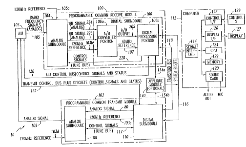
Figure 1 is a block diagram illustrating a
c
S~
-
CA 02230~60 1998-02-26
W O 97/08843 PCTAJS96/14165
programmable radio system 10 which includes a
programmable common receive module (PCRM) 100 and a
programmable common transmit module (PCTM) 102.
The PCR~M 100 comprises an analog S~ Alll e 104
and a digital submodule 106.
The analog submodule 104 receives radio
frequency signals within a range of interest, in
this example, approximately 2 MHz to 2000 MHz. The
analog submodule 104 is described in related U.S.
disclosure entitled WIDE-_AND RADIO-FREQUENCY
COh Vl~;K'l'~;~ H~VING MULTIPLE USE OF lN~ IATE
FREQUENCY TR~NSLATORS.
The digital submodule comprises an analog to
digital converter (ADC) portion 106a and a digital
processing portion 106b, electrically isolated from
each other.
The PCTM 102 is partitioned into an analog
submodule 108 and a digital submodule 110. The
p~vyr - ~hle common transmit module (PCTM) 102 is
described in related U.S. disclosure entitled COMMON
TRA~SMIT MODULE FOR A PRO~RAMMART~ DIGITAL RADIO.
The PCTM 102 is not used for receive only radio
functions, such a& present for an Instrument T.An~; ng
System.
A system bus 116 couples the PCRM 100 and the
PCTM 102 to external devices. More specifically,
the system bus 116 connects the digital submodule
106 of the PCRM 100 and the digital submodule llo of
the PCTM 102 to external devices such as a computer
112 with associated devices such as a UART 114, a
sound card 120, and memory 122. The memory 122 may
be used for storing application programs which may
be downloaded to the PCRM 100 and the PCTM 102 via
the system bus 116.
As more fully explained in the related U.S.
SUB~5T~UTE SHEET ~ E 263
CA 02230~60 1998-02-26
W O 97/08843 PCT~US96/14165
- 16 -
disclosure entitled DIGITALLY PROG~AMMART~
MULTIFUNCTION RADIO SYSTEM ARCHITECTURE, in some
applications the PCRM 100 and the PCTM 102 are
directly connected to other modules needed for
additional message processing, security purposes or
for interfaces to various st~n~A~d buses. These
additional modules may additionally be connected to
the system bus 116. Also, as explained in the same
U.S. disclosure, the system bus 116 and any other
buses described herein can be physically partitioned
into separate buses for control ~_ ~n~, message
data, spare buses, etc.
Further, a transpond bus 118 may, for example,
connect the PCRM 100 ~o the PCTM 102; and an antenna
interface unit (AIU) control bus 130 may connect the
PCRM 100 to an associated AIU 103n, in this example,
AIU 103. A transmit control bus plus various
discretes 132 connect the PCTM 102 to the associated
AIU 103n. As explained in the related U.S.
disclosure entitled DIGITALLY PRO~RAMMART~
MULTIFUNCTION RADIO SYSTEM ARCHITECTURE, in a rare
case where the digital submodule 106 has
insufficient processing capacity to perform a higher
level of signal processing directly on a received
waveform, prior to demodulation and subsequent
reduction to a relatively low-speed serial bit
stream ouL~uL, applique buses 134a and 134b connect
PCRM 100 and PCTM 102 to an optional applique module
140 which performs such processing.
Not all of the above external buses are used
for every radio application. For example, radio
functions requiring an applique bus 134a or 134b
generally do not require a transpond bus 118.
A tune bus 228 connects the digital submodule
106 of the PCRM 100 (via the digital processing
~TiT~T_ ~E~ ~ L~
CA 02230~60 l998-02-26
W O 97/08843 PCT~US96/14165
portion 106b) to the analog submodule 104 of the
PCRM 100. Further, although not shown, those of
skill in the art can utilize the programmability of
the hardware described herein and include additional
interconnections between the digital processing
portion 106b of the digital submodule 106 of the
PCRM 100 to the analog submodule 104 of the PCRM
100 .
The PCRM 100 is preferably comprised of a
single module (a plug-in module for many
applications) that receives RF (analog) signals from
an antenna interface unit (AIU) 103, described in
more detail in the related architecture disclosure;
DIGITALLY PROGRAMMART~ MULTIFUNCTION RADIO SYSTEM
ARCHITECTURE, or a signal distribution network. The
PCRM 100 outputs relatively low-speed serial digital
data. Inside the PCRM 100, RF signals are frequency
translated through various intermediate frequencies
(IFs), digitally sampled and processed according to
the CNI programmed configuration, and routed to an
appropriate digital GuL~uL. Con~; ~nt of the
major signal operations in a single programmable
unit greatly facilitates logistics, built-in
test/fault-isolation test (BIT/FIT) and maintenance,
and produces savings due to economy of scale.
Figure 2 is a diagram illustrating the
connection of the PCRM 100 to the AIU 103. The AIU
103 may, for example, include a first antenna
interface unit (AIU) 103a and a second antenna
interface unit (AIU) 103b coupled to a switch 154.
The PCRM 100 can be configured as part of a first
channel 156 formed by connecting the PCRM 100 to
first AIU 103a via switch 154, or as part of a
second ~-h~nnel 158 formed by connecting the PCRM 100
to second AIU 103b via switch 154. Thus, the PCRM
SUE~STITUT~ S~IEET ~
CA 02230~60 1998-02-26
WO 97/08843 PCT~US96/14165
- 18 -
100 can be configured to be one ch;~nnel of a
plurality of ch~nnel 5,
A similar configuration is possible for
connecting the PCTM 102 to AIUs, in this example,
two AIUs, as disclosed in detail in the related
disclosure COMMON TRANSMIT MODULE FOR A PROGRAMMARLE
DIGITAL RADIO.
Figure 3 provides a more detailed drawing of
the digital 511' - ~ 1 e 106. The digital submodule
106 of the programmable common receive module (PCRM)
100 can service a wide range of CNI functions,
including AIR TRAFFIC CONTROL RADAR BEACON,
INSTRUM~NT LANDING SYSTEM, VHF RADIO and others as
detailed in the related DIGITALLY PROGPAMMART-~
MULll~u~CTION RADIO SYSTEM ARCHITECTURE disclosure.
The flexible and functionally efficient digital
processing architecture provided by the digital
submodule 106 includes a combination of functional
hardware elements such as, for example, one or more
ADCs, including a 8-bit wide band ADC 200 operating
at 40 MHz and a 14-bit narrow band ADC 202 operating
at 4 MHz; one or more reconfigurable format units,
commonly referred to as field-programmable gate
arrays or similar dynamically configurable units
such as FPGA1 206, FPGA2 212 and FPGA3 214; one or
more dynamically configurable digital downconverters
(DDC) with associated filtering/decimation units
such as DDC 210; one or more sequential and/or
parallel instruction processors sometimes referred
to as central processing units (CPUs) or digital
signal processors (DSPs) such as DSP 216; memory
such as random access memory (RAM) 220; and
nonvolatile memory (FLASH) 222; one or more
dynamically configurable programmable digital filter
units, with either serial or parallel I/O such as
SU~STITUT~ SHEET ~Ui -~
CA 02230~60 1998-02-26
W O 97/08843 PCTrUS96/14165
-- 19 --
PDFU 230; and receivers, transmitters and/or
transceivers for I/0, such as, for example, line
transceivers 215 and 217.
The digital submodule receives an analog signal
224 or 226 from the analog submodule 104 that is
band limited to either wide band or narrow band,
respectively. This signal is supplied to the A/D
Converter Portion 106a of the digital submodule 106.
If the signal is wide band, it may be, for example,
an IF (intermediate frequency) wide band signal
limited to +4000 kilohertz about 30 MHz, resulting
in a total of 8 MHz of IF bandwidth maximum. If the
signal is narrow band, it may be, for example, an IF
narrow band signal limited to +200 kilohertz about 1
MHz, resulting in a total of 400 kilohertz of IF
bandwidth maximum.
In this example, two analog to digital
converters (ADC) are used: one for converting a
narrow band (NB) signal 202 and one for converting a
wide band signal (WB) 200. Specifically, a wide
band signal (WB) 224 at 30 MHz is supplied to an 8-
bit 40 MHz wide band analog to digital converter (WB
ADC) 200 such as, for example, an AD9012AJ from
Analog Devices. By utilizing well-known 4/3
harmonic sampling (i.e., the sampling of the 30 MHz
I/F signal at a sample rate of 40 MHz), the wide
band signal at 30 MHz is folded down to the 10 MHz
region.
A narrow band (NB) signal 226 is supplied to a
14-bit 4 MHz narrow band analog to digital converter
(NB ADC) 202 such as, for example, an ADS944MC from
Datel. The signal flow for various RF input ranges
and radio function types within the analog submodule
104 is discussed in the related U.S. disclosure
entitled WIDE-BAND RADI0-FREQUENCY CO~V~K1~ HAVING
SUB~IT~ITE ~;HE~ U~
CA 02230~60 1998-02-26
W O 97/08843 PCT~US96/14165
- 20 -
MULTIPLE USE OF lNl~MEDIATE FREQUENCY TRANSLATORS.
Both the WB ADC 200 and the NB ADC 202 are
coupled to a converter switch (SW) 204 or a
multiplexer which controls which signal is
transferred to the L~ q;n;ng portion of the digital
submodule 106, i.e., the digital processing portion
106b. The SW 204 is controlled by switch control
bits which indicate whether the WB 224 or NB 226
signal is to be transmitted to the digital
processing portion 106b. If the NB signal 226 is
selected, the data received from the NB ADC 202, in
this example 14 bits of data, are transmitted with a
data valid bit and a clock bit to a first field
programmahle gate array (FPGAl) 206 as a selected
digital signal. In the alternative, if the WB
signal 224 is selected, the data received from the
WB ADC 200, in this example 8 bits of data, are
transmitted with a data valid bit and a clock bit to
the first FPGAl 206 as the selected digital signal.
In the present invention, three FPGAs 206, 212
and 214 are used to perform selected operations.
The FPGAs may be, for example, Altera Flex Parts
81188. The function of these FPGAs is controlled by
configuration data which is set forth in the
appendix. As discllc-c~A later, ultimately, these
three FPGAs could be combined into a single, and
p~hApc more flexible, unit.
The first FPGA (FPGAl) 206 will receive the
selected digital signal and dep~nA;ng upon the
application selected and the chip configuration
program loaded, perform specified functions or
operations which may include, for example, data
reformatting, parallel to serial conversion and
vice-versa, control, pulse width discrimination,
interval discrimination, mode d~coA;ng, pulse
SUB~iT~UTE ~;~tEEr ~RU~ ~ 2F~'
CA 02230~60 1998-02-26
W O 97/08843 PCT~US96/14165
- 21 -
detection, and other types of signal processing.
One specific example is when data from either
WB ADC 200 or NB ADC 202 are routed to the DDC 210.
The FPGA1 206 reformats the data into a format
required for input to the DDC 210, for example, into
16-bit parallel data which includes 14 bits of data
from NB ADC 202 plus the data valid bit and the
clock bit. The clock bit may be derived from the
on-board clock.
In another example, if the data includes 8-bit
parallel data from WB ADC 200, the 6 least
significant bits (LSBs) of the 14-bit parallel data
are merely ignored.
The FPGA1 206 may additionally reformat output
data received from the DDC 210 prior to routing the
data to another unit within the digital submodule
106. Specifically, the GuL~uL from DDC 210 is, in
this example, typically 20 bits in serial form. The
FPGAl 206 may, for example, serial-to-parallel
convert the data ouL~uL and add proper 12 LSB of the
data o~L~uL to the data ouL~uL for consistency with
a 32-bit local bus 218.
In another example, if serial data output from
DDC 210 is to be input to a programmable digital
filter unit (PDFU) 230, the FPGA1 206 may then
reformat the data output to be consistent with input
requirements for the PDFU 230, i.e., if necessary,
add (or truncate) an appropriate number of bits and,
also if necessary, serial-to-parallel convert the
data ouL~uL if the PDFU 230 requires a parallel
input.
The digital down converter (DDC) 210, such as,
for example, a HSP50016 chip manufactured by Harris
Semiconductor, is coupled to an A/D converted output
from switch 204 via FPGAl 206 and to the local bus
~UBSTI 1 l.lTE S~EET (P~l IL'~
CA 02230~60 1998-02-26
W O 97/08843 PCTnUS96tl4165
218 via FPGAl 206. The DDC 210 may be used, for
example, to perform frequency down conversion, fine
~lln; n~, filtering and decimation of the selected
digital signal. The software executable to perform
the down conversion, filtering and decimation for
each application is set forth in the appendix.
The processor (DSP) 216 may be, for example, a
TMS320C31 chip. The DSP 216 may perform various
processing functions on various types of signals
which may, for example, include signals associated
with various narrow band and wide band radio
functions. The processing functions may include,
for example, decimation filtering; waveform
demodulation of any combination of amplitude,
frequency and phase modulation; signal correlation;
squelch; management and control of all channel
resources (gain, signal path switching, tuning,
interfaces both internal to the PCRM 100 as well as
to external units, etc.) in both the digital
submodule 106, the analog submodule 104 and the
associated AIU 103 (Figure l); bit stream decoding
including error detection and/or correction; BIT
control/reporting; Fourier transforms; calculations
of difference in depth of modulation (DDM); and
formatting control for various te- i n~l ~ such a~
displays. Further, although sometimes performed
elsewhere in the receive channel, the DSP 216,
~pen~ i ng upon the processing power implemented, can
perform ?r~Age processing, network functions, and
processing of low-data rate speech algorithms.
Software for performing the functions of AM
demodulation, decimation, fourier transforms,
difference in depth of modulation and display
functions in the DSP 216 is set forth in the
appendix. The remaining functions may be easily
~3UE~S i ITUTF ~
CA 02230~60 1998-02-26
W O 97/08843 PCTrUS96/14165
- 23 -
,.
progrA ~~ by one skilled in the arts.
A second FPGA (FPGA2) 212 may be pL~yLammed to
be configured, for example, to perform interface
operations between the local bus 218 and several
elements of the digital submodule 106. Further, the
FPGA 212 may also, for example, perform interface
operations to a system bus 116, a transpond bus 118
and an applique bus 134a via transceivers located in
a multi-transceiver package 217.
A third FPGA (FPGA3) 214, also coupled to the
local bus 218, may be configured to perform RF
control functions, including providing control bits
via a tune bus 228 to the analog submodule 104 of
the PCRM 100 through, for example, a transceiver in
a multi-transceiver package 215; and via an AIU
control bus 130 to the associated AIU 103 also
through, for example, a transceiver in the multi-
transceiver package 215. The FPGA3 214 may also be
configured to perform control functions of various
elements of the digital s-~ le 106 by providing
control bits.
In addition, memory may be coupled to the local
bus 218 and may include, for example, a 128K bits x
32 bits wide random access memory (RAM) 220 and a
128K bits x 32 bits wide non-volatile memory such as
the ~_ -n "FLASH" memory or EEPROM (FLASH) 222.
The RAM 220 and the FLASH 2 22 are used to store
application specific information, including FPGA
configuration data, used during initialization and
when switching applications.
The digital submodule 106 may be configured to
perform specific functions depending on an
application desired. The structure of the digital
submodule 106 permits changing the configuration to
perform a different application within a very short
SUBSTIT~TE S~EET (P~U~
CA 02230~60 l998-02-26
W 097/08843 PCT~US96/14165
- 24 -
period of time, without requiring a change in
hardware.
One method to allow for this quick
reconfiguration is the following. An external
device 112, such as a CNI controller (e.g., computer
112), is programmed to control the DSP 216. The
external device then downloads application
information, including programs and data files for
each of the FPGAs 206, 212 and 214, regarding each
application which may be desired to be performed by
the PCRM 100, over the local bus 218 to the RAM 220.
This downloading process to RAM 220 takes, in this
example, approximately 100 milliseconds for a 1
megabit/sec serial system bus 116.
The DSP 216 then executes a RAM program which
instructs the DSP 216 to copy corresponding
application information to the FLASH 222. If time
is critical, a selected application program can be
tely run from RAN 220 and later transferred
to the FI-ASH 222 when convenient.
When power to a board with the digital
submodule 106 is disconnected and the power is
reapplied to the board, a boot program instructs the
DSP 216 to copy application information and a
corresponding application program from the FI-ASH
222, into the RAM memory 220 based on an application
selected. The application is selected through
selection data received over the system bus 116.
The corresponding application program pertA; n; ng to
the selected application then executes from the RAM
220.
Each program pert~;n;ng to the selected
application includes source code for running the DSP
216 and data files for each of the FPGAs 206, 212
and 214 and the DDC 210, if applicable.
~UBS~TUT~ EET (RVL~
CA 02230~60 1998-02-26
W O 97/08843 PCTrUS96/14165
Reconfiguring the PCRM 100 for a selected
application from the RAM typically takes place in
approximately 50 milliseconds in the existing
embodiment. The appendix sets forth example code
for functions performed by the FPGAs 206, 212 and
214.
Therefore, each FPGA 206, 212 and 214 is
transferred gate configuration information
pert~;n;ng to the specific application selected when
the power is initialized. Additionally, the
selected application may be altered any time during
use. New selection data, indicating that a new
application is being selected, is received from the
system bus 116. The DSP 216 receives the new
selection data, recognizes that the currently
selected application is to be changed to a newly
selected application, determines the location in the
RAM 220 of the newly selected application, reads
application information from the location of the RAM
220 per~;ning to the newly selected application,
and transfers the read application information to
each of the FPGAs 206, 212 and 214. Each FPGA is
then reconfigured to perform specific functions as
specified for the newly selected application.
As mentioned previously, the external device
112 may be, for example, a CNI controller, a mass
memory storage unit or a computer. Additionally,
the outside device 112 may be, for example, on-board
or off-board. If the external device 112 is a
c~ luLer, the computer may be directly coupled to
either the local bus 218 or DSP 216. For example,
an external memory 122 associated with computer 112
may consist of nonvolatile memory such as PROMs,
EPROMs, FLASH, hard disk and floppy disk, and/or
volatile memory such as RAM. Nonvolatile memory can
;~iU~TiTUT~ SHcEl ~.V~
CA 02230~60 1998-02-26
W O 97/08843 PCTrUS96/14165
- 26 -
permanently contain all software applications and
associated data for the entire digitally
programmable radio system, including all software
applications for the PCRM 100. Floppy disks, for
example, may then be used to import new or modified
software applications.
For rapid downloading to the PCRM 100 and to
other programmable system modules, application
information to be downloaded may be first
transferred from a slower-access memory, such as
hard or floppy disk to RAM. The downloading occurs
via the system bus 116, which may be segregated into
separate buses for signal data and for module
control including downloading.
A flexible I/0 configuration provided in the
digital Sll~ oAlll e 106, for example, by the FPGA2 212
under control of the DSP 216, can provide a
downloaded data format consistent with a choice of
the computer 112. When multiple application
programs are already resident in the RAM 220 of the
digital submodule 106, the computer 112 may download
brief code corresponding to a particular
application. The brief code instructs the digital
submodule 106 to configure its elements for a
designated application. The designated application
can be determined, for example, either by an
external control device such as a keyboard or
touchscreen (not shown) via an external control
interface 126, or, for example, by an automatic
resource reconfiguration algorithm such as when the
PCRM 100 functions as a spare PCRM and is
automatically reprogrammed to replace a failed PCRM
configured to receive and process a particular radio
function.
The various external interfaces to the digital
~B~TlTUTE ~HEET ~RLIL~ ~B~
. CA 02230~60 1998-02-26
:
submodule 106 are completely programmable in a same
or similar manner as the digital submodule 106 is
programmable for various radio functions.
Specifically, external I/O programming and
configuration data can be downloaded to the RAM 220
from an external unit, such as, for example, the
computer 112, via, for example, the system bus 116
or, if partitioned separately., a control/data bus as
described in the related U.S. disclosures DIGITALLY
PROGRAMMABLE MULTIFUNCTION RADIO SYSTEM ARCHITECTURE
and COMMON TRANSMIT MODULE FOR A PROGRAMMABLE
DIGITAL RADIO.
With regard to external connections, I/O
configuration data is used to configure -
reconfigurable format units, in this example, the
FPGAs 212 and 214, to route digital bitstreams to
and ~rom each external interconnection utilized.
The flow of digital signals with respect to the
external interfaces, including the electrical
formats (bit length, bit rate, etc.) and protocols,
is under control of a sequential/parallel
instruction set processor which is in this example,
~ DSP 216.
Thus, the common receive module 100, and
particularly the digital submodule 106, has
programmable external interfaces that can be used
for a variety of interface applications, including
control functions and signal flow. The programmable
external interfaces may be serial or parallel,
synchronous or asynchronous, unidirectional or
bidirectional, and include standard and/or custom
protocols. However, including elements necessary to
meet special physical interface requirements for all
types of external connections in the common receive
module 100 may not be practical. Such elements may
_
-
CA 02230~60 1998-02-26
. .
- '
~ ,
- 28 -
include isolation transformers or drivers to meet
voltage levels required by various bus standards.
In many cases such elements are not required; the
external connections run to other system units of
the digitally programmable radio system, and the
external interfaces and connections of these system
units have the same physlcal definitions. However,
where such elements such as application transformers
or drivers of a different line voltage level are
~~ 10 required in a system application, these elements are
contained externally in bus interfaces units as
described in the related U.S. disclosure DIGITALLY
PROGRAMMABLE MULTIFUNCTION RADIO SYSTEM
ARCHITECTURE.
In addition, major portions of the analog and
digital submodules 104 and 106, respectively, can be
combined in higher levels of integration. For
example, all field programmable gate arrays (FPGAs)
206, 212 and 214 may be combined into a single
element or "chip," or the entire digital circuitry
including the FPGAs, the digital downconverter (DDC)
210, the DSP 216 and the memory 220 and 222 can be
= consolidated into a single element for possible
savings in size, cost and power dissipation.
As illustrated in Figure 3, high-speed sampling
rate synchronous control processing (such as A/D
conversion by ADCs 200 and 202; down conversion and
decimation by DDC 210; waveform processing by DSP
216; bit stream processing by FPGAs 206, 212 and
214) and high-speed parallel interconnects, such as
A/D buses 201, 203 and 205, high-speed preprocessor
and DDC bus 211, DSP (i.e., CPU) data and addr~ss
buses, collectively called a local bus 218, and FPGA
buses 213a, 213b and 213c, described later, are
contained inside the PCRM 100. This greatly
CA 02230~60 1998-02-26
W O 97/08843 PCT~US96/14165
- 29 -
simplifies backplane complexity, and reduces
electromagnetic interference (EMI) to the rest of
the digitally programmable radio system 10. The
PCRM 100 handles internal EMI between analog and
digital circuitry using separate circuit boards,
shielding and isolation.
The internal processing performed among various
elements in the digital submodule 106, as described
above, is referred to as sampling rate synchronous
control processing. This processing is required to
receive an analog IF signal from the analog
submodule 104 and to condition the IF signal into a
digital information signal suitable for use by
various external units such as those associated with
the C~r- uLer 112 or information tel in~ls, as
described in the related U.S. disclosure DIGITALLY
PRO~,~AMMARTT" MULll~uNCTION RADIO SYSTEM
P-~C~TTECTURE.
As also described in the related U.S.
disclosure the digital information signal may also
be routed to the PCTM 102 by the transpond bus 118
if the common transmit module 102 is employed for a
transponder or repeater function, or routed to an
applique -~tlle 140 via an applique bus 134a if a
special processing applique unit 140 is employed to
perform signal processing such as low probability of
detection (LPD) processing that is beyond the
processing capability of the digital submodule 106.
One of the key objects of this invention is to
contain sampling rate synchronous control within the
PCRM 100 and, specifically, within the digital
submodule 106 to simplify external interconnections
among system units by utilizing serial interfaces of
as low a speed as possible for the external buses of
relatively long physical length, i.e., the system
iTiTUT~ Si~E~T ~
CA 02230~60 1998-02-26
- 30 -
bus 116, which may be segregated into separate buses
as noted above. The optional higher-speed parallel
transpond bus 118 and the applique bus 134a, both of
which, in this example, are infrequently used, are
of relatively short physical length due to the close
proximity of the other system units utilizing these
buses. Moreover, the transpond bus 118 and the
applique bus 134a, although of higher speeds, are
asynchronous to avoid sending a higher speed clock
over an interconnection between system modules.
Such simplification of external interconnections
also reduces electromagnetic interference (EMI)
problems and improves the reliability of the
physical interconnections among units. Simplified
interconnections are particularly important if such
system units are of a plug-in variety, where
deterioration of plug-in connectors over time and
with usage decreases system reliability and
increases EMI.
Additionally, to ~urther reduce EMI between
digital circuitry and the relative sensitive analog
_ elements in any transmit or receive channel in the
~ overall system, and with respect to any control-type
bus that connects the digital submodule 106 to such-
analog elements, clocks that may be associated with
such control-type buses are turned off after passage
of control data has been completed. For example, if
the AIU control bus 130, which provided tuning
. and/or other control information to the AIU 103, is
implemented to include a separate differential clock
line, the clock is disabled after the control
~ information is passed to the AIU 103. ~Similarly, a
clock associated with the tune bus 228 can be turned
off after passing tuning and/or other type of
- 35 control information from the digital submodule 106
-
CA 02230~60 1998-02-26
W O 97/08843 PCTrUS96/14165
to the analog submodule 104.
The analog and digital submodules 104 and 106
of the PCRM 100 (and those of the PCTN 102) are
preferably implemented on separate circuit boards.
For purposes such as fabrication, testing, etc., the
analog and digital submodules 104 and 106,
respectively, can reside on the same circuit board
but with electrically isolated analog and digital
portions. Alternatively, each submodule (104 and
106) may be multiple physically separate circuit
boards properly connected. "Circuit board" is a
general term encompassing numerous forms of
cont~; -nt such as "chips," application-specific
integrated circuits (ASICs), monolithic hybrid
packages (MHPs), etc.). In this example, an analog
portion would include elements of the analog
submodule and the A/D converter portion 106a,
including the ADCs 200 and 202, from the digital
submodule 106, in this example, the digital
processing portion 106b. The digital portion would
include the rem~;n;ng elements of the digital
submodule 106.
The ADCs are necessarily a part of the analog
portion. The ADCs 200 and 202 are powered from the
analog power source and are electrically isolated
from the other elements of the digital sub -~1l1 e. A
reference signal (e.g., 120 MHz) is transmitted from
the analog submodule 104 to the ADCs of the digital
submodule 106, is suitably divided (e.g., by 3 to 40
MHz) and is transmitted via differential lines to
the digital processing portion 106a with its
separate power/ground system of the digital
submodule 108. These ADCs 200 and 202 could be, for
example, on an analog submodule board of PCRM 100.
However, in this example, the ADCs 200 and 202 were
SU~ST~TUTE~ tET (F.L7L-~
CA 02230~60 1998-02-26
WO 97/08843 PCTAJS96/14165
- 32 -
included on the digital s~ d~le board for space
considerations.
Regardless of the specific ?c-h~n;cal
configuration of the analog and digital submodules
104 and 106, respectively, the analog and digital
portions are electrically isolated from each other
in order to prevent relatively noisy digital
circuits from creating unwanted extraneous signals
within sensitive analog circuits. A conductive
shield and possibly a frame of a material, such as
mu-metal or aluminum, is preferably provided between
the boards. Analog signals between the boards are
generally not transmitted over co~ l cables.
To provide further isolation, the digital and
analog portions preferably have separate power
sources and ground lines (different ground planes)
to prevent noise and ground loop problems through
the power supply. To further prevent noise problems
digital signals transmitted between the analog and
digital portions and external conne~tions~ are
differential (dual rail) signals. In addition,
high-speed digital clocks associated with digital
circuitry in the analog submodule 104, such as a
clock for the tune bus 228, are turned off during
signal reception.
The above isolation and power/ground
considerations enable high speed (e.g., 40 MHz)
digital circuits to be placed in the same relatively
small box as the sensitive analog receive module
elements.
An explanation of the use of the external bus
connections is now given. For further explanation
of the external bus connections described below
refer to the related U.S. disclosure entitled
DIGITALLY PROGRAMMART~ MULTIFUNCTION RADIO SYSTEM ARCHITECTURE.
SUBSTI~U T - S~E~T ~R~
CA 02230~60 1998-02-26
WO 97/08843 PCT~US96/14165
The system bus 116 is primarily used to:
(1) Pass demodulated message data from the PCRM
106 to the e~ternal device 112, such as a computer,
associated units, and/or to other external devices
not shown;
(2) Pass control data (frequency channel,
antenna selection, etc.) and radio application
software programs from an external controller (e.g.,
computer 112) to the PCRM 100; and
(3) Pass channel status information collected
in the PCRM 100 to the external controller 112. In
some applications, the system bus 116 can serve as a
multiple access ~~~Age (i.e., intercom) bus among
various radio channels and various external user
stations (not shown) coupled to the system bus 116.
In other applications, and as explained in the
related U.S. disclosure DIGITALLY PROGRAMMART~
MULTIFUNCTION RADIO SYSTEM ARCHITECTURE, an o~L~L
of the PCRM 100 may first pass through another
module which is dedicated to a same channel to
perform additional --~ge processing and/or
security functions such as decryption on the
relatively low-speed serial bit stream. As
explained in the related U.S. disclosure entitled
DIGITALLY PROGRAMMART~ MULTIFUNCTION RADIO SYSTEM
ARCHITECTURE r if bus traffic warrants, the system
bus 116 can be physically partitioned into separate
buses, e.g., for control/status, one or more buses
for message data to and from information te~ ;nA 1 5
and spare buses for redundancy. (For additional
description of system bus partitioning, please refer
to the related U.S. disclosure entitled DIGITALLY
PROGRAMMART~ MULTIFUNCTION RADIO SYSTEM ARCHITECTURE
and COMMON TRANSMIT MODULE FOR A PROGR
DIGITAL RADIO.)
~ lr ~EL~
CA 02230~60 1998-02-26
W O 97/08843 PCTnUS96/1416
- 34 -
The system bus 116 is preferably differential
(i.e., dual rail) for better noise immunity;
however, the system bus 116 can also be configured
as single ended for some applications by bypassing
line transceivers 217 in the digital suL ~ le 106
associated with the system bus 116. Also, the
system bus 116 is preferably configured to be
asynchronous, i.e., performing a UART (Universal
Asynchronous Receiver/Transmitter) function,
although the system bus 116 can also be synchronous
by providing an associated clock line.
An AIU control bus 130 is a bidirectional bus
that, depending upon the radio application, passes
control information to the associated AIU 103 in the
same ch~n~l, to include, for example: initiation of
built-in-test (BIT), filter tuning information,
automatic gain control settings based upon received
signal level, and relatively slow switching either
for antenna selection or for the distribution of the
AIU RF ouL~uL to various PCRMs 106(n). Also, the
AIU bus 130 passes information (e.g., BIT status)
from the AIU 103 to the PCRM 100 and ultimately to
the external controller 112.
When implemented for a particular radio
function, a transpond bus 118 can be used for
various purposes such as for a radio transponder
which is described later herein as well as in the
related U.S. disclosure entitled DIGITALLY
PROGRAMMARTT~ RADIO MODULE FOR TRANSPONDER SYSTEMS.
Additionally, usage of the transpond bus 118, such
as in a radio repeater application, is explained in
the related U.S. disclosure entitled DIGITALLY
PROG~AMMARTT'' MULTIFUNCTION RADIO SYSTEM
ARCHITECTURE.
Depending upon the application, the transpond
SUBS, iTU--I t Sl~ E~ E ~
CA 02230~60 1998-02-26
W O 97/08843 PCTAJS96/14165
bus 118 may be a serial or multibit parallel bus
~ (e.g., of several bits) and of differing speeds
(e.g., 10 MHz). The FPGAs 212 and 214 may, for
example, for~at a digital bit stream in the
appropriate format and line drivers (e.g.,
transceivers, receivers) and provide differential
connections for improved noise ; ;ty. The
transpond bus 118 is preferably configured to be
asynchronous, e.g., performing a UART (Universal
Asynchronous Receiver/Transmitter) function.
As explained in the related U.S. disclosure
entitled DIGITALLY PROG~AMMART~ MULTIFUNCTION RADIO
SYSTEM ARCHITECTURE, in a rare case where the
digital sllh Jdule 106 has insufficient processing
capacity to perform a higher level of signal
processing directly on a received waveform prior to
demodulation and subsequent reduction to a
relatively low-speed serial bit stream output, the
applique buses 134a and 134b connect the PCRM 100
and the PCTM 102 to an optional applique module 140.
In this caser the applique module 140 will perform a
higher level of signal processing, such as for
waveforms of low probability of detection (LPD)
type. The input/ouL~uL configuration of the
applique buses 134a and 134b is similar to that of
the transpond bus 118, in that the applique buses
134a and 134b are multi-bit parallel buses of
moderate speed (e.g., 10 MHz), and preferably
asynchronous. Further, the external connections are
differential for improved noise immunity.
Depending upon the applique application
selected to be performed by the applique -Allle 140,
various routing and processing options are
available. For example, a (nominally wide band)
signal received and routed through the analog
TU~ r T~R~i~ 2c-'
CA 02230~60 1998-02-26
W O 97/08843 PCT~US96/14165
- 36 -
5~ le 104 to the wide band ADC 200 can be
connected directly to the applique bus 134a and to
the applique module 140 through the switch 204, the
FPGAs 206 and 212, and the transceivers 217.
Alternatively, desired preprocessing of the signal
ouL~uL from the WB ADC 200 can be performed by any
of the processing elements such as the DDC 210, the
PDFU 230 or the DSP 216. After being processed in
the applique module 140, the signal can either pass
directly to the system bus 116 or the signal can be
routed back to the PCRM 100 for additional
processing before being routed to the system bus
116. Other routing options are also possible based
on the interco~ection wiring among the various
modules in the overall system.
A tune bus 228 pAC~es control information from
the digital submodule 106 to the analog submodule
104. The tune bus 228 is preferably configured to
be synchronous. A differential control line bus
pair plus a differential clock signal may be sent
along a separate line pair (not shown), although the
tune bus 228 could also be configured to be
asynchronous if desired. If the differential clock
signal is used, it is turned off after data transfer
to prevent corruption of the sensitive analog
circuits of the analog portion of the PCRM 100
during signal reception.
As noted previously, not all external buses are
used for every radio application. In addition,
those of skill in the art can configure the FPGAs to
supply interfaces with other units, where such
interfaces may be serial or parallel, unidirectional
or bidirectional, synchronous or asynchronous as
warranted, to include both stAn~d or custom
protocols. I/O pins may be included on a PCRM I/O
S~.lBSTiTU I E S~ UI E ~ ~
CA 02230~60 1998-02-26
,~
- 37 -
connector. These I/O pins can be utilized as any of
the buses noted herein or as additional buses
defined by the user. How the buses are employed,
their physical implementation as serial or parallel,
and connections to other modules may be determined
by a module interconnection scheme (e.g., wiring
harness, backplane) used by a system application
desired by a user.
Figure 4 is a block diagram of the analog
_ 10 submodule. An RF/IF conversion scheme for reception
of a signal in an approximate input frequency range
of 2-2000 MHz is described in the related U.S.
disclosure entitled WIDE-BAND RADIO-FREQ~ENCY
CONVERTER HAVING MULTIPLE USE OF INTERME~IATE
FREQUENCY TRANSLATORS.
Control o~ the analog submodule via tune bus
228 is now described. After receiving tuning
information and/or built-in test (8IT) initiation
from the system bus 116 via the FPGA 212 of the
digital submodule 106 (Figure 3) and the local bus
218, the DSP 216 of the digital submodule 106
~ (Figure 3) calculates and proportions tuning between
- an NCO 254 in the DDC 210 of the digital submodule
106 (shown, for example, in Figure 8), and a tunable
local oscillator #1 (LO1) 1004 in the analog
submodule 104, shown in Figure 4. The DSP 216
(Figure 3) uses the tuning information for the
analog submodule 104 to determine, preferably using
a lookup table although calculations may be used,
control settings for switches 1250a through 1250f,
programmable dividers 1252a and 1252b.
Additionally, the DSP 216~(Figure 3) uses the
tuning information to determine on/off settings for
output dividers 1254a, 1254b, 1254c and 1254d and
optional divider 1254e and switch 1256. If BIT
~ . . . - , , .~5;,
CA 02230~60 1998-02-26
- 38
initiation is also requested, a switch 1280 is
controlled such that a noise diode 1260 supplies an
input test signal through various paths of the RF/IF
frequency translator chain. In additlon, based upon
either a tuning versus control voltage estimate or
actual calibration data from voltage-controlled
oscillators (VCOs) 1262a and 1262b, the DSP 216
(Figure 3) calculates and determines digital control
inputs to digital-to-analog converters (DAC preset)
1264a and 1264b to provide rapid preset tuning
voltages for VCOs 1262a and 1262b. As a result,
rapid tuning for a double phase-locked loop (DPLL)
synthesizer 1226 is also provided. Implementation
of rapid tuning presets for phase-locked-loops is
well known to those of skill in the art.
Further, settings of any automatic gain control
within the RF/IF frequency translator chain (e.g.,
control of NAGC 1200) or a gain control element in
the AIU 103 is also determined based upon signal
level measurements, in the DSP 216 of the digital
submodule 106 (Figure 3).
_ As shown in Figure 3, control information such
- as described above is passed to the FPGA 214 in the
digital submodule 106 over, for example, the local
bus 218, ~ormatted into a serial bit stream and
passed through a differential line transceiver in
the transceivers unit 215 to the tune bus 228. The
information on the tune bus 228 is received by a
control interface 240 in the analog subm~odule 104.
As shown in Figure 5, the control interface 240
is preferably comprised of line receivers 1242 such
as, for example, an SN7~1570 available ~rom Texas
Instruments; an electronically programmable logic
~ device (EPLD) 1244 such as, for example, a CY7C343
available from CYPRESS; and a decoder 1246 such as,
CA 02230~60 1998-02-26
W O 97/08843 PCTrUS96/14165
- 39 -
-
for example, a 74LS139 available from Texas
InstLI -nts~ Control GuL~uLs from either the EPLD
1244 or the ~eco~e~s 1246 are distributed to various
controlled elements of the analog submodule 104
described above. Such distribution and control are
well known to those of skill in the art.
In addition, (not shown) a separate
differential clock signal for the tune bus 228 may
also be sent from the digital submodule 106 to the
EPLD 1244 in analog submodule 104. After passing
the control information from the digital submodule
106 to the analog submodule 104 via the tune bus
228, an associated differential clock signal is
turned off during signal reception to avoid clock
contamination of the relatively sensitive analog
circuits.
Also not shown are return signals that those of
skill in the art can implement to enhance operation
of the PCRM 100. For example, one of these return
signals could be a status signal indicating lock up
of the DPLL 1226. In this example, the status
signal is obtained from a programmable divider 1252a
(such as cont~ine~ in Qualcomm part 3036 which also
contains a phase/frequency detector 1253a) and is
passed through an ECL gate (not shown) and sent back
to the digital submodule 106 as a differential
signal for improved noise immunity. Ultimately, the
differential signal is passed on to a system
indicator (not shown) associated with a system
controller such as the computer 112.
The analog submodule 104 also contains anti-
aliasing fi]ters to process received signals before
delivery to the ADCs 200 and 202 in the digital
submodule 106.
Specifically, a primary anti-aliasing filter
SUE~ST~TUTE ~;HEE~ U~
CA 02230~60 1998-02-26
.
- 40 -
preceding the WB ADC 200 is bandpass filter (BPF)
1251 located in the analog submodule 104. BPF 1251
is preferably chosen to have a passband bandwidth of
8 MHz but can be chosen with a wider or narrower
bandwidth depending upon the selected group of
application. A primary anti-aliasing filtering
preceding the NB ADC 202 for this process is
bandpass filter (BPF) 1257 (preferably 800 KHz)
located in the analog submodule 104, although the
. . _
'-_ 10 appropriate path BPF either in a switched filter
bank 1255 (e.g., approximately 100 KHz, 200 KHz or
400 KHz depending upon the application) and BPF 1259
(preferably 400 KHz) also provide a degree of
anti-aliasing.
Additionally, those of skill in the art can
utilize the programmability of the hardware
described herein to include additional
interconnections between the digital submodule 106
of the PCRM 100 (via the digital processing portion
106b) to the analog submodule 104 of the PCRM 100.
The present configuration of the PCRM 100
allows for execution of built-in tests. Built-in
- test (BIT) can be easily performed on the entire
PCRM 100. For example, referring to Figure 3, an
external source such as that associated with the
computer 112, would request BIT for the PCRM 100.
The BIT request is passed to the DSP 216 via the
system bus 116, one of the line transceivers in the
l.ine transceiver package 217, the FPGA 212, and the
local bus 218. The DSP 216 then initiates the
request. The noise diode 1260 (Figure 4) inputs a
noise test signal via switch 1280 in analog
submodule 104.
The noise test signal is routed through the
RF/IF chain of the analog subnodule 104, to one of
-
CA 02230~60 1998-02-26
W O 97/08843 PCT~US96/14165
- 41 -
the ADCs 200 or 202. The noise test signal is
further routed through various paths which may
include, for example, the DDC 210, the PDFU 230, the
FPGAs 206, 212, 214, the FLASH 222, the RAM 220, or
the DSP 216. The PCRM 100, or portions thereof, is
then determined to be functional or not functional
depending upon whether the signal generated by noise
diode 1260 is ultimately received in digital
submodule 106 and a receive-signal indication given
to computer 112.
The unique, flexible and functionally efficient
digital processing architecture includes the
functionality such as that provided by units such as
the DDC 210, the FPGAs 206, 212 and 214, the PDFU
230, the DSP 216, the FLASH 222 and the RAM 220, as
described herein, which can be programmed by those
of skill in the art, particularly with the
application notes available with these various
units, to perform various processing functions on
various type signals, including signals associated
with various NB and WB radio functions, where the
processing functions include, for example, I/Q
partitioning, frequency translation, decimation,
filtering, and waveform demodulation of any
combination of amplitude, frequency and phase
modulation, pulse width and interval detection and
discrimination, mode (e.g., interrogated mode)
decoding, signal reformatting, signal correlation,
fine frequency hopping (coarse frequency hopping is
performed in the analog submodule 104), squelch,
channel control (e.g., gain, signal path switching,
tuning) in both the digital s~ e 106, analog
submodule 104 as well as the associated AIU 103, bit
synchronization, bit stream decoding including error
detection and/or correction, flexible I/0
SUB~ITl~TE S~trET ~ L~
CA 02230~60 1998-02-26
WO 97/08843 PCTrUS96/14165
- 42 -
configuration for all interfaces both internal to
the PCRM 100 and to external units,
management/configuration of all the PCRM 100
resources, and BIT control/reporting. Additionally,
although sometimes performed elsewhere, the PCRM
100, depending upon the processing power
implemented, can perform message processing
including reformatting, network functions,
deinterleaving, processing of low-data rate speech
algorithms, and formatting for various terminals
such as displays. All of these example processing
functions as well as other achievable processing
functions can be ~uickly reprogrammed under internal
or external control over a wide range of parameters.
For example, the ~LoyLdmmable Common Digital
Receiver 100 may perform CNI radio applications such
as, for example, Instrument T~ing System (ILS),
Air Traffic Control Radar Beacon System (ATCRBS) and
VHF AM radio which are discussed in more detail
hereinafter.
The ILS ~;~c~ ion gives an example of
processing associated with time-multiplexed
amplitude modulated narrow band signal functions.
The ATCRBS discussion gives an example of processing
associated with pulse modulated wide band signal
functions. The VHF AM ~;~Ccllc-cion gives an example
of processing associated with a voice-modulated
function.
Also see the related U.S. disclosure entitled
WIDE-BAND RADIO-FREQUENCY CO~V~K'1'~K HAVING MULTIPLE
USE OF lNl~ ~IATE FREQUENCY TRANSLATORS for a
description of the signal flow for a wide variety of
radio functions, including the above radio
functions, through the analog submodule 104. Those
of skill in the art can program the digital
~Ui~ T_ S{~cET ~2~L~- ~ri
CA 02230~60 l998-02-26
W O 97/08843 PCTAUS96tl4165
- 43 -
submodule 106 to process the signals output by the
analog submodule 104, such that the overall PCRM 100
can receive, process and demodulate a wide variety
of signals of any combination of amplitude,
frequency and phase modulation, including signals
associated with a wide variety of NB and WB radio
functions.
Additional modifications easily made by one
skilled in the art include, for example, as shown in
Figure 3, the programmable digital unit(s) (PDFU)
230, such as, for example, an HSP 43124 available
from Harris Semiconductors. The PDFU 230 may be
used to obtain additional programmable filter
parameters independent of filter parameters in the
DDC 210 that are tied to DDC decimation rates.
These PDFUs 230 may provide such filtering more
efficiently in hardware than can be provided in the
DSP 216. By connecting the PDFU 230 to the FPGA1
206, for example, which serves as a signal
reformatting and routing unit, the PDFU 230 can be
inserted at various locations in the signal flow.
For example, the PDFU 230 could receive a signal
from one of the ADCs 200 and 202, provide an output
to one of the various buses, such as, for example,
the system bus 116, and the transpond bus 118
through the FPGA2 212.
In this example, the PDFU 230 HSP43124 is a
serial I/O unit for size considerations.
Additionally, the FPGAl 206 functions as a parallel-
to-serial (and vice versa) converter. However, a
parallel I/0 PDFU unit could be employed to reduce
overall delay time. Although, in this example, the
hardware to be resident in every digital submodule,
the hardware used may depend on the system
application if desired. Further, depending on the
~U&S~-ITU~E S~EET ~PiU' ~ o ~
CA 02230~60 1998-02-26
- 44 -
system application to be performed, specific
hardware units may be changed, added or eliminated.
Additionally, improved analog units may be
located in the analog submodule 104 and improved
digital units may be located in the digital
submodule 106, for example, to reduce size, cost and
power dissipation, or to improve performance such as
finer tu~ing steps in the tunable LO1 1004 (Figure
4) in the analog submodule to reduce the re~uired
-_ 10 filter width in the analog RF/IF filters. A/D
converters of faster sampling rates and/or higher
dynamic range may also be issued.
A method for extending the frequency-coverage
of analog submodule 104 is given in the re1ated U.S.
disclosure WIDE-BAND FREQUENCY CONVERTER HAVING
MULTIPLE USE OF INTERMEDIATE FREQUENCY TRANSLATORS
below 1.5 MHz down to at least 1 KHz. This extends
fre~uency coverage of common receive module 100 to
at least 1 KHz, which enables RF functions such as
Omega navigation, Loran-C and Automatic Direction
Finding (ADF) to be serviced. With reference to
_ Figure 4, the RF input to analog submodule 104 is
received from an AIU, such as AIU 103, which is
tailored to conditi~n specific RF functions as
described in the related U.S. disclosure DIGITALLY
PROGRAMMABLE MULTIFUNCTION RADIO SYSTEM
ARCHITECTURE. This conditioning for all radio
functions, including those below 1.5 MHz, generally
includesJ as a minimum, RF filtering and, if needed
for the particular RF function(s) being serviced,
may also include signal amplification and control of
channel gain.
The RF input passes through SP2T switch 1280 as
described in the related U.S. disclosure WIDE-BAND
FREQUENCY CONVERTER HAVING MULTIPLE USE OF
.CA 02230~60 1998-02-26
-,
, ,
- 45 -
INTERMEDIATE FREQUENCY TRANSLATORS. The output
switch 1280 is connected to an input of SP2T switch
1290. The switch 1290 has two outputs, one of
which, 1071, passes to frequency translator 1002 and
which is used to service the RF ~unctions between
approximately 1.5 MHz and 1870 MHz as described in
the related disclosure. Also, instead of
transmitting the 1 MHz output, described in the
related disclosure, directly to the 14-bit ADC 202
....
: 10 in digital submodule 106, the 1 MHz output 1294 is
connected to the input of SP2T switch 1296.
When servicing the RF functions described in
the related disclosure, external commands such as
from computer 112 are passed to digital submodule
106 in a manner similarly described and then relayed
to analog submodule 104 via tune bus Z28. Control
interface 240 then commands switch 1296 to connect
output 1294 to the 14-bit ADC 202. On the other
hand, when servicing RF functions below 1.5 MHz,
external commands flow in the same manner except
that switch 1296 is commanded to connect output 1294
_ of switch 1290 to the 14-bit ADC 202, in which case
~~ the RF input 1000 is connected to the 14-bit ADC
202. Because-ADC 202 is sampled as 4 MHz, it can
service RF ~unctions below 1.5 MHz.
Also described in the above two related
disclosures is a method for extending the upper
frequency range of the programmable common receive
module 100 above 1870 MHz to 3500 MHz.
Another change might be, for example, to change
the line receiver 1242 (Figure 5) in the analog
-~ubmodule 104 to a line transceiver similar to one
located in the line transceivers unit 215 (Figure 3)
such that information from the analog submodule 104
could be passed back to the digital submodule 106
~ S~
CA 02230~60 1998-02-26
W O 97/08843 PCTrUS96/14165
- 46 -
along the tune bus 228 for status or processing
purposes.
Functional unit capacity can be added, either
through additional or larger capacity units such as
the DDC 210, the PDFU 230, the FLASH 222, the RAM
220, the DSP 216, and the FPGAs 206, 212 and 214.
Additional capacity could be added to transceivers
such as 215 and 217 for additional I/Os to external
units or between the analog submodule 104, digital
to analog converter portion 106a and the digital
processing portions 106b of the PCRM 100. Moreover,
any or all of these functional units such as the
FPGAs 206, 212 and 214, or the ADCs 200 and 202
could be consolidated into units of larger
functional usage, in order to reduce overall size
and also to reduce costs such as resulting from
fewer parts count and large scale manufacturing of
units that are common among a wide variety of radio
applications and a wide variety of integrated system
applications.
-Specifically, as technology improves it is
anticipated that the ADCs 200 and 202 of the PCRM
100, can be replaced by a dual mode ADC that can
operate at both of the required rates or perhaps at
a single rate (e.g., the 40 MHz rate) provided the
NB ADC 202 dynamic range requirements can be met for
the NB signals, such as by using the AD9042
available from analog devices which provides 12 bits
at 40 Mhz. In this latter case the 40 MHz sampling
rate is decimated to 4 MHz to maintain compatibility
with the digital down conversion and to
approximately maintain the same dynamic range (via
the decimation process) as the 14-bit NB ADC.
Moreover, a higher speed ADC such as AD 9042 could
also be used to sample both the WB IF output (e.g.,
SuBs~ F S'rlEET ~ IL~
CA 02230~60 l998-02-26
'. :
-- 47 --
at 30 MHz) and the NB IF output (e.g., at 1 MHz) and
thus require only a single ADC. The higher dynamic
range of this high-speed (e.g., 40 MHz) ADC would be
sufficient to eliminate a sequential detection log
video amplifier (SDLVA) 1261 and associated
circuitry in analog submodule 104 (Figure 4).
However, an IF limiter could still be employed to
replace the limited IF output 1261a. Also, use of a
higher (e.g., 40 MHz) sampling rate for the 1 MHz IF
output path instead o~ a lower (e.g., 4 MHz)
sampling rate does not necessitate that L03 signal
input to multiplier 1021 ( Figure 4) be an exact
multiple (e.g., 32 MHz) o~ the lower sampling rate
to cause aliased ADC sample harmonics to-fall at
zero Hz, thus simplifying L03 (in this example
allowing L03 to be equal to 30 MHz) and replacing
the relatively complex circuits o~ the multiplier
1265 and the divider 1267 with a simpler divide-by-4
(not shown). In this latter case, a band pass
filter (BPF) 1269 at 32 MHz would be replaced with a
BPF at 30 MHz. In addition, as technology improves
it is anticipated that the A/D conversion can be
~ done prior to various downconverting stages
performed in the analog submodule 104.
Additionally, the DSP 216 may include more than
one processor depending on the desired functions to
be performed.
The individual functions described herein of
the recon~igurable ~ormat unit, which is, for
example, comprised of the FPGAs 206, 212 and 214,
can be modified or rearranged among the different
FPGAs by the programmer. Additionally, the
functionality described herein can also be included
into a single large FPGA when such single large FPGA
exists. Further, a single or multiple FPGAs can be
.
-
CA 02230~60 1998-02-26
W O 97/08843 PCTrUS96/14165
- 48 -
programmed by those of skill in the art,
particularly with the application notes available
with these units, to perform not only the functions
previously described for the FPGAs 206, 212 and 214
but, as later noted, other functions in conjunction
with the unique, flexible and functionally efficient
digital processing architecture described herein
consisting of the various functionality provided by
units such as the DDC 210, the FPGAs 206, 212 and
214, the PDEU 230, the DSP 216, the FLASH 222 and
the RAM 220.
Moreover, FPGAs need not be used, but instead,
any devices which perform these types of functions
may be substituted. As noted previously, not all
external buses are used for every radio application.
In addition, those of skill in the art can configure
the FPGAs to supply interfaces with other units,
including the interfaces described previously, where
such interfaces may be serial or parallel,
unidirectional or bidirectional, synchronous or
asynchronous as warranted, to include both standard
or custom protocols. The I/O pins are included on a
PCRM I/O connector, and these pins can be utilized
as any of the buses noted herein or as additional
buses defined by the user. How the buses are
employed, their physical implementation as serial or
parallel, and their connections to other modules are
determined by the module interconnection scheme
(e.g., wiring harness, backplane) that is employed
by the system application desired by the user.
None of the above changes, additions or
deletions of any of the functionality for reasons
such as improved performance, size, cost or power
dissipation will invalidate the unique
analog/digital architecture disclosed herein, in
SUE~STI~UT_ SI~EEr (RU~ ~ 28~
CA 02230~60 1998-02-26
WO 97/08843 PCTrUS96/14165
- 49 -
-
particular the unique, flexible and functionally
efficient flexible digital processing architecture
disclosed herein.
Inst,. -nt T~n~;ng System (ILS) Application:
In ILS processing, three radio functions,
namely Localizer (LOC), Marker Beacon (MB) and
Glideslope (GS), are time interleaved in an RF
signal received by the PCRM 100.
Prior to operation, the configuration programs
for the LOC, MB and GS radio functions comprising
the ILS application are placed in the RAM 220 as
previously explained, either by downloading from
external memory over the system bus 116 or from the
FLASH memory 222. These three radio functions are
time interleaved into RF signals received and
processed by the PCRM 100.
The analog 511~ -lle 104 and the digital
submodule 106 are each sequentially configured and
tuned to route and process each of the ILS radio
functions in a repetitive time multiplex sequence
described later. For example, the analog submodule
104 is sequentially configured and tuned to receive
each ILS function signal, frequency translate each
ILS function signal, and route the translated ILS
function signal to the NB IF ou~L at preferably 1
MHz. (Functional routing through the analog
submodule 104 of a wide variety of radio functions,
including the ILS radio functions, is described in
the related U.S. disclosure entitled WIDE-BAND
RADIO--FREQUENCY CONV~;~'l'~;~ HAVING MULTIPLE USE OF
EDIATE FREQUENCY TRANSLATORS.)
The translated ILS function signal is passed to
an ADC, such as the NB ADC 202, preferably sampled
at 4 MHZ. As previously described, the translated
~l~BSTlTUT~ SHEET ~RU~ ~ 2~)
CA 02230~60 1998-02-26
_
_
- 50 -
ILS ~unction signal could be sampled at higher
rates, for example in an ADC sampled at 40 MHz that
~ replaces both the WB ADC 200 and the NB ADC 202 with
a single unit. A converted ILS signal is passed to
the digital processing portion 106b of the digital
submodule 106 which is also sequentially configured
to process the same radio function passed through
the analog submodule 104. A signal o~ each selected
function of the ILS application is received for a
. 10 preset amount of time. The analog submodule 104 and
the digital submodule 106, are then reconfigured to
a new selected ILS radio function and the new
selected function is received for a preset amount of
time. The sequence is then repeated. -
Figure 6 illustrates an example of an
individual TDM (Time Division Multiplex) sequence
for the processing of the ILS radio functions. The
time sequence consists of "sampling" periods and
"tune" periods. The sampling periods are shown as
"LOCALIZER," "MB," and "GLIDESLOPE." The tune
periods are shown as "TUNE."
_ At start-up, and based upon control information
-- received via the system bus 116 from the control
. (not shown) associated with computer 112, the DSP
216 calculates, proportions and stores the tuning
requirements between coarse tuning in the analog
submodule 104 and fine tuning in the DDC 210 of
digital submodule 106 for each of the radio
functions that are time multiplexed. The analog
submodule 104 and the digital submodule 106 are then
configured and tuned to receive the LOC signal. In
addition, during each subsequent tune period, the
analog submodule 104 and the digital submodule 106
are.configured (including tuning) to receive a next
signal to be processed. By the end of the tune
., ~, . _ ..
CA 02230~60 1998-02-26
- . ,.
period, the PCRM 100 has been tuned to receive the
desired signal, the ADC 200 is sampled at the
~ desired rate, for example at 4 MHz, and the DDC 210
is downconverting and decimating (i.e., reducing the
sample rate) as later described.
No start bits or framing bits are required to
initiate or synchronize the ILS processing.
Synchronization of hardware in the PCRM 100 is
accomplished by allowing enough time in the tune
_ 10 period for the hardware to reconfigure for a new
operating mode. The sampling periods for LOC, GS
and MB end when a desired number of samples are
received, which may differ for each radio function.
The length o~ the tune period is controll-ed by timer
interrupts generated in the DSP 216. When a timer
runs out, the tune period ends and a next sampling
period begins.
In this example, at start-up, as previously
noted, the analog submodule 104 and the digital
submodule 106 are configured and tuned to receive
the LOC signal. Processing begins with a 33.36 msec
LOC period. A 6.5 msec tune period follows. During
this tune period, the LOC processing completes and
the analog submodule 104 and digital submodule 106
are configured to receive the MB signal. A 10 msec
MB period occurs, followed by a 4 msec tune period,
during which the MB processing completes and the
analog submodule 104 and the digital submodule 106
are configured to receive the GS signal. A 33.36
msec GS period occurs, followed by a 4 msec tune
period, during which the GS processing completes and
the analog submodule 104 and the digital submodul,e
106 are configured to receive the LOC signal. A
33.36 msec LOC period occurs, followed by a 6.5 msec
tune period, during which the LOC processing
CA 02230~60 1998-02-26
W O 97/08843 PCTrUS96/14165
- 52 -
completes and the analog s~ 1l1 e 104 and digital
submodule 106 are configured to receive the MB
signal. A 10 msec MB period occurs, followed by a 4
msec tune period, during which the MB processing
completes and the analog submodule 104 and the
digital submodule 106 are configured to receive the
LOC signal.
The LOC and MB functions require a somewhat
higher cycle rate than the GS function in order to
process the audio tones associated with the LOC and
MB functions. An entire sequence takes 145.08 msec
and is repeated as shown in Figure 7. Four
different wait periods, the values of which have
been predetermined by systems analysis and
comprising a "jitter", are inserted prior to
starting the next sequence in order to reduce the
effects of synchronous AM noise sources such as
aircraft propellers. The four different wait
periods likewise repeat in the same order. In this
example, the four wait periods are 3 msec, 12 msec,
15 msec and 8 msec, respectively. An entire
sequence repetition thus takes 618.32 msec to
complete.
Figure 8 illustrates signal flow for an ILS
application. Major components in the ILS digital
receive signal path are the NB ADC 202, the FPGAl
206, the FPGA2 212, the FPGA3 214, the DDC 210, and
the DSP 216. Although not utilized in the following
embodiment, PDFUs 230 may be employed for more
efficient or additional digital filtering, as
previously discussed. The NB ADC 202, receives an
analog input signal and ouL~uLs digital data
samples. The FPGAl 206 controls data flow between
the NB ADC 202, the DDC 210, the DSP 216 and, if
employed, the PDFU(s) 230. The FPGA2 inputs
SUB5~1TU~F ~tE~ ~R' 1' ~ 5~!
CA 02230~60 1998-02-26
W O 97/08843 PCTrUS96/14165
- 53 -
-
parallel data and transmits serial output data onto
system bus 116. The DDC 210 performs downconversion
and decimation. For the ILS application, the DSP
216 performs signal processing, including envelope
detection, filtering, AGC, Discrete Fourier
Transform (DFT), threshold detection, d~co~;ng, and
message formatting. Also if desired, algorithms for
other functions such as automatic frequency control
(AFC) can be easily implemented by those of skill in
the art.
For example, AFC could be performed by routing
output from the DDC 210 through the FPGA1 206 to the
DSP 216 which, perhaps in conjunction with the FPGAs
206, 212 and 214, performs an AFC algorithm that
derives a tuning error. The tuning error is then
used to correct tuning of the DDC 210. The
flexibility of the processing architecture disclosed
herein permits some of these DSP operations to be
performed in other units if desired such as in the
FPGAs 206, 212, 214, and, if employed, the PDFU(s)
230.
The digital submodule 106, via the FPGA3 214,
also controls resources of an associated channel,
including the analog submodule 104 via the tune bus
228 and the AIU 103 associated with the ~h~nnel via
the AIU control bus 130. Such control information
is either derived internally by the digital
submodule 106 which provides settings for automatic
gain control (AGC) based upon received signals
levels, or is derived externally to provide tuning
information via the system bus 116 from, for
example, a control (not shown) associated with the
computer 112.
All external interfaces to the digital
submodule 106 through the FPGA2 212 and the FPGA3
SUE~;~lTU-~ E St~EET ~PiULE ~
CA 02230~60 1998-02-26
W 097/08843 PCTAUS96/14165
- 54 -
214 are via the line trAnC~;vers 217 and 215. Use
of the line transceivers 217 and 215 improves
electrical isolation previously described in
conjunction with descriptions of the tune bus 228
and the AIU control bus 130.
The FPGA3 214 iS coupled to the local bus 218
and the tune bus 228. The FPGA3 214 performs
receiver control functions in response to a control
word received from the DSP 216 over the local bus
218. Software in the DSP 216 formats a tune word
which includes tuning information and other
information such as switch settings for IF signal
routing in the analog ~111 ~ule 104 and AGC levels.
The DSP 216 transmits the tune word to the FPGA3
214. The FPGA3 214 then transmits the tune word
data serially over the tune bus to the analog
submodule 104 as previously described. In the
existing embo~ rt the tune word is 56 bits;
however, the flexibility of the processing and
control architecture disclosed herein permits words
of different size based upon future requirements
such as finer steps in the tunable LO1 270 of the
analog submodule 104. Also, different tune words
can be sent at different rates for different
functions. For example, a single tune word need
only be sent for a PCRM that is set at a single
frequency for a relatively long period. on the
other hand, AGC updates may be sent at modest rates.
Similarly, control information is sent to the
AIU 103 associated with the channel via the AIU
control bus 130. The control information sent
depends upon the overall system design for the ILS
function. For example, the AIU control information
can include automatic gain control (AGC) settings
based upon a received signal level. Also, control
SUB~T~TE S~ !L~ &3
CA 02230~60 1998-02-26
W O 97/08843 PCTrUS96/14165
- 55 -
signals could switch inputs from LOC, MB and GS
r ante~n~ in synchronism with processing performed in
PCRM 100. On the other hand, such antenna inputs
may be merely added via an RF summer unit or
frequency multiplexer, as is well known to those of
skill in the art. However, switch control signals
could route the LOC, MB and GS signals through
different paths, e.g., for different filtering and
amplification. In addition, in order to meet
stringent interference requirements, tuning
information could be supplied to tunable
preselectors in the AIU 103.
After the analog submodule 104 has been tuned
to the desired frequency, the analog signal is
received and down-converted in the analog submodule
104 and then ou~u~. The output of the analog
submodule 104 is a narrow band signal (NB) 226,
preferably, for example, near 1 MHz, that is sent to
an ADC such as the 14 bit, 4 MHz NB ADC 202. Data
samples are routed through the switch 204 to the
FPGAl 206. Data is latched into the FPGAl 206 on a
low-to-high transition of a data valid signal from
the ADC 202. The FPGAl 206 then ouL~uLs the latched
data in its internal register to the DDC 210.
Synchronization is achieved by using an input clock
to the DDC 210 derived from the data valid pulse and
a clock such as a 40 MHz clock.
The digital signal samples are then provided to
the DDC 210 for digital down conversion. For ILS
processing, the DDC 210 accepts real input data
samples at selected frequency, for example a signal
near a 1 MHz frequency that is sampled at a 4 MHz
input sampling rate.
The DDC 210 generates pairs of in-phase (I) and
quadrature phase (Q) data that are frequency
T~U~E S5~ UL-~
CA 02230~60 l998-02-26
W097/08843 PCT~US96/14165
- 56 -
downconverted (i.e., translated) to baseband (i.e.,
centered on DC) via a sinusoid generator, referred
to as a numerically controlled oscillator (NCO) 254,
which generates both in-phase (I) (i.e., cosine) and
quadrature phase (Q) (i.e., sine) local oscillator
signals, and I and Q digital mixers 250 and 252.
The step size of a tunable LO1 270 in the analog
submodule 104 is not sufficiently fine to frequency
translate every LOC and GS ~hAnnel (as well as
channels for other radio functions) to the same
frequency, for example, 1 MHz, at the output of the
analog submodule 106; therefore, most LOC and GS
channels will possess slightly different frequencies
(e.g., offset from 1 MHz) at the input to the DDC
210. This offset is acc-- ~dated by tuning the NCO
254, which typically has more than adequate tl-ning
resolution of less than 1 Hertz, to a frequency of
the real input data sample input to the DDC 210.
The I represents the real, mixed cosine or
"in-phase" part of the data and Q represents the
imaginary, mixed sine or "quadrature" part of the
data. The I and Q data are then decimated (i.e.,
the sampling rate is reduced) from the input
sampling rate (e.g., at 4 MHz) to an output I/Q pair
rate of 25 KEIZ or 50 KHz, for example, depending on
the ILS processing mode. The ouL~L decimation
rates are chosen to provide at least a Nyquist
sampling rate for the signal bandwidths of interest,
including frequency drift. For ILS, for example,
these bandwidths may be 2 5 KEIZ for the LOC and MB
signals, and 50 KHZ for the GS signal.)
Additionally, the DDC 210 includes filters, an
output formatter, and control logic.
Frequency translation tuning to baseband and
decimation rates are controlled by control words
~UB~ TE S~ RUL~ ~?
CA 02230~60 1998-02-26
,
- 57 -
loaded into the DDC 210 during the tune period. The
disclosed processing architecture permits various
- methods for loading these control words depending
upon the brand of hardware elements chosen for the
DDC 210 and DSP 216. For example, control data
words can be downloaded in parallel format over the
local bus 218 to the FPGA1 206, parallel-to-serial
converted in the proper serial ~ormat, and loaded
into a control I/F port (not shown) of the DDC 210
to control DDC tuning, decimation rates, number of
output bits, output data format, etc., as allowed by
the specific DDC hardware.
On the other hand, as in the described
embodiment, the DSP 216 provides a serial~ output
(not shown) specifically for loading control-type
data to other devices such as the DDC 210. In this
case the serial output from the DSP 216 may either
be connected directly to the DDC 210, if the serial
bus formats can be made compatible by programming
the DSP 216 and/or the DDC 210, or the serial
control connection can be routed through the FPGA1
206, which reformats the control data into a form
: suitable for the DDC 210.
~ Outputs from the DDC 210 are transferred back
to the FPGA1 206. The DDC outputs include I/Q data
and, in the preferred embodiment, a synchronization
clock signal and a real control signal for each
sample. The clock signal is generated by the DDC
210. The rea~ control signal indicates whether the
output data is real (I) or imaginary (Q). The I/Q
data from the DDC 210 (e.g., serial 20-bit data) is
received by the FPGA1 206, formatted into~a data
word usable with the local bus 218 (e.g., formatted
via serial-to-parallel conversion into a 32-bit data
word usable with the TMS-320 C31 DSP) and latched
.
-'''i~~J-t ~ S
_
CA 02230~60 1998-02-26
W O 97/08843 PCTrUS96/14165
- 58 -
into a register in the FPGAl 206. Then, the FPGA1
206 raises a sampling interrupt in the DSP 216,
signalling that a sample is available. The software
in the DSP 216 responds to the sampling interrupt by
reading data from an address mapped into a register
in the FPGAl 206 containing the data sample. The
data read from the FPGAl 206 is then stored in the
RAM 220 prior to processing in the DSP 216.
An example of processing in the DSP 216 is
illustrated in Figure 9 and Figure 10. All of the
operations noted on these figures are performed by
software loaded in the DSP 216. The processing is
described below for each ILS operating mode.
As illustrated in Figure 9, in step Sl during
LOC processing, sampling interrupts will occur every
20 usec, corresponding to a 50 KHz rate. A complete
I and Q data pair will therefore be received every
40 usec, corresponding to a 25 KHz rate.
As shown in Figure 10, envelope detect 300
performs an envelope detect operation on each pair
of I and Q data samples. The output of the envelope
detect 300 is a real-valued signal magnitude. A
total of 834 magnitude samples will be collected
during the 33.36 msec LOC sampling period (Figure
9). The magnitudes are then filtered and decimated
by LOC filter/decimate 302a, to reduce the number of
data samples to be proc~e~. Decimation by a
factor of 3 re~llce~ the number of magnitude samples
from 834 to 278 and the sample rate to 8.333 KHz. A
decimated G~L~uL signal is produced.
In step S2 for LOC processing, and during the
MB tune period (Figure 9), an LOC discrete fourier
transform unit LOC DFT 306a (Figure 10) performs
278-point DFT at 0 Hz, 90 Hz, 150 Hz and 1020 Hz on
the decimated output signal to produce 0 Hz, 90 Hz,
t3UE~STITlJTE S~EET ~R~
CA 02230~60 1998-02-26
W O 97/08843 PCTrUS96/14165
150 Hz and 1020 Hz ouL~uLs. The 0 Hz, 90 Hz, 150 Hz
ouL~uLs of the DFT are supplied to LOC
difference-in-depth-of-modulator, LOC DDM 308, which
performs a DDM processing to produce a DDM result.
The 1020 Hz DFT ouL~uL is used by an identification
decoder 314 to decode a station ID morse code. A
DDM result from LOC DDM 308 is filtered by a LOC
Filter 312 to dampen effects of any transients in
the DDM result. Also, measurement of a signal level
of the DDM result is used for AGC settings as
desired by the user. For example, for AGC settings
in the analog sni -~le 104 and, if desired, for AGC
settings in the AIU 103 associated with the ch~n~el.
The AGC settings are preferably determined by a
lookup table in the RAM 220 based upon signal
strength level.
Use of DFT 306a measurements for AGC will set
AGC levels according to in-c-hAnn~l signal strength.
Other signal monitoring methods for AGC are possible
as desired during system design. For example, a
signal level on the ADC 202 can be monitored
directly, e.g., by monitoring an ADC MSB, in order
to set AGC levels according to the total signal
level, both in-chAnnel and out-of-channel, incident
on the ADC 202. The LOC DDM ouL~Ls are formatted
and placed in a system bus --c~ge for tr~n~ ;~~ion
to an external ILS display device via the system bus
116. The Station ID morse code can be transmitted
by various methods and as desired by the system
designer according to a chosen protocol for the
~ystem bus 116. These methods include:
(1) Passing individual pulses of the station ID
morse code to the external computer 112 for decoding
and subsequent audio output via a sound card 120
and/or display on a display unit 126;
3TlTUTE ~t~EET (RlJ~
CA 02230~60 1998-02-26
W O 97/08843 PCTAUS96/14165
- 60 -
(2) Storing an entire station ID morse code
sequence of the code pulses in the RAM 220 prior to
transmitting the station ID morse code sequence to
the computer 112 for decoding, etc.;
(3) Digitally forming tones and transmitting
the tones to sound card 120 to produce an audio
output, and, if desired, for decoding and subsequent
display on display unit 126.
Also during step S2 (Figure 9), appropriate
resources in the analog submodule 104, the digital
submodule 106 and the AIU 103 associated with the
channel are selected and tuned under control of the
DSP 216 using data transmitted over associated buses
as previously described, in this case to receive and
process the signal for the MB channel.
Reconfiguring the FPGAs 206, 212 and 214 when time
multiplexing among the LOC, MB and GS functions is
not necessary.
During the next tune period for LOC, e.g., in
step S6 (Figure 9), the LOC AGC data is passed, if
desired, to the analog sl~ ~~ le 104 via the tune
bus 228 and, also if desired, to the AIU 103
associated with the channel via AIU control bus 130.
In step S3 during MB processing, sampling
interrupts will occur every 20 usec, corresponding
to a 50 KHz rate. A complete I and Q data pair will
therefore be received every 40 usec, corresponding
to a 25 KHz rate. The envelope detector 300 (Figure
10) performs an envelope detect operation on each
pair of I and Q data samples. The ouL~uL of the
envelope detector 300 is a real-valued signal
magnitude. A total of 250 magnitude samples will be
collected during the 10 msec LOC sampling period.
The magnitudes samples are then filtered and
decimated by a MB filter/decimate 302c to reduce the
SUBST5TUTE S~ RLIL~ 2~'3
CA 02230~60 l998-02-26
WO 97/08843 PCT~US96/14165
- 61 -
number of data samples to be processed and a
decimated signal is produced. Decimation by a
factor of 2 r~fl~lçe~ the 1~ h~ of magnitude samples
from 250 to 125 and a sample rate of the decimated
signal is reduced to 12.5 KHz. The decimation
factor is chosen to reduce the number of MB samples
to a whole number for processing simplicity while
still maintaining a sufficiently high sample rate
and number of samples.
In step S4 (Figure 9) a 125--pointDFT is
performed by a MB DFT 306c at 0 Hz, 400 Hz, 1300 Hz,
and 3000 Hz to produce DFT results. The DFT results
are used by a MB Detector 320 to detect via a
threshold setting, a presence of an outer (400 Hz),
a middle (1300 Hz), and an inner (3000 Hz) MB tone
and thus, produce MB ouL~Ls. The MB outputs are
then formatted and placed in a system bus message
for transmission to the external ILS display device
126 and the external tone generator which is not
shown but preferably included in sound card 120. If
desired by the system application, tones can be
formed digitally and transmitted to the sound card
120 similar to that described in conjunction with
the VHF AM description, described later.
Additionally, if desired by the system
application, AGC can be performed similar to AGC for
the L~OC function and AGC data can be sent to
appropriate unit (e.g., analog s~ le 104 and/or
AIU 103) during the next MB tune period, for example
in step S8 ~Figure 9). Also during step S4,
appropriate resources in the analog submodule 104,
digital submodule 106 and the AIU 103 associated
with the channel are selected and tuned under
control of the DSP 216 via data transmitted over
associated buses as previously described, in this
SU~isTIT~)TE~tEET~RUL ~'
CA 02230~60 1998-02-26
W O 97/08843 PCTrUS96/1416
- 62 -
case to receive and process the signal for the GS
channel.
In step S5 (Figure 9) during GS processing,
sampling interrupts occur every 10 usec,
corresponding to a 100 KHz rate. A complete I and Q
data pair will therefore be received every 20 usec,
corresponding to a 50 KHz rate. The envelope
detector 300 (Figure 10) performs an envelope
detector operation on each pair of I and Q data
samples. The output of the envelope detector 300 is
a real-valued signal magnitude. A total of 1668
magnitude samples are collected during the 33.36
msec GS sampling period. The magnitude samples are
then filtered and decimated (GS Filter/Decimate
302b) to reduce the number of data samples to be
processed. Decimation by a factor of 6 reduces the
number of magnitude samples from 1668 to 278 and
reduces the sample rate to 8.333 KHz.
In step S6, a GS DFT 306b performs a 278-point
DFT at 0 Hz, 90 Hz, and 150 Hz. The 0 Hz, 90 Hz,
150 Hz ouL~uLs of the DFT are used by a GS DDM 316
to c: ~ùLe a GS difference-in-depth-of- modulation
and produce a DDM result. The DDM result is
filtered by a GS Filter 318 to dampen the effect of
any transients in the DDM result and GS outputs are
produced. The GS outputs are formatted and placed
in a system bus ?scAge for transmission to an
external ILS display device interface such as
Display I/F 126. If desired by the system
application, AGC can be performed similarly to that
performed for the LOC function and AGC data can be
sent to an appropriate unit (e.g., the analog
submodule 104 and/or the AIU 103) during the next MB
tune period. Also during step S6, appropriate
resources in the analog submodule 104, the digital
SUB~TUT~ S~ RU~ ~ 2~,
' CA 02230~60 1998-02-26
W O 97/08843 PCTAJS96/14165
- 63 -
-
submodule 106 and the AIU 103 associated with the
channel are selected and tuned under control of the
DSP 216 via data p~F~ over the associated buses as
previously described, in this case to receive and
process a signal for the LOC ch~nnel~
Steps S7 through S10 repeat steps Sl through
S7, respectively, with the entire sequence of steps
Sl through S6 being repeated during a period the
digital submodule is configured for the ILS
application.
Data is output over the system bus 116 using
the Universal Asynchronous Receiver Transmitter
(UART) capability programmed into FPGA2 212. Figure
11 is a block diagram of the FPGA2 212. The FPGA2
212 receives an 8 bit data word 440, and loads it
into the 8-bit buffer 420 with a transmit load data
(TLD) signal 442. The TLD signal 442 is derived
from an address decode of the buffer l420 address.
When the software in the DSP 216 writes to the
address of buffer 420, the TLD signal 442 will be
set. A FULL signal 454 is derived from control
logic in a format unit 424. The FULL signal 454 is
set when a new byte is deposited into the buffer
420.
If a shift register 422 is empty, the byte in
the buffer 420 will be transferred in parallel to
the shift register 422. When data is transferred
into the shift register 422, the FULL signal 454
will be reset and an interrupt 460 will be sent to
the DSP 216 indicating that the buffer 420 is empty
and ready for a new byte. If the shift register 422
is not empty, the transfer of the next byte into the
shift register 422 from the buffer 420 will not
occur until the last bit of the shift register 422
is shifted out. The format unit 424 uses signals
SUBST~TUTt S~tEET ~R~
CA 02230~60 1998-02-26
W O 97/08843 PCT~US96/14165
- 64 -
baud rate CLK 452, and a digital submodule clock 107
of, for example, 40 MHz, provides synchronization of
data flow between the buffer 420, the DSP 216, and
the shift register 422.
By the process described above, an In~trument
T.~n~;ng System which performs efficiently and
accurately can be achieved within a programmable
common receive module. Those of skill in the art
can use the above description plus application notes
and functional requirements documents to use or
modify the programmable common receive module
disclosed herein for reception and processing of
other time-interleaved waveforms including various
combinations or amplitude, frequency and/or phase
modulated waveforms.
Air Traffic Control Radar Beacon System
(ATCRBS) Application:
In ATCRBS processing different modes of
interrogation may be processed.Prior to operation,
configuration programs comprising the ATCRBS
application are placed in the RAM 220 as previously
explained, either by downloading from external
memory over the system bus 116 or from the FLASH
memory 222. The analog submodule 104 and the
digital submodule 106 are each sequentially
configured and tuned to route and process ATCRBS
interrogations.
Figure 12 illustrates the signal flow through
the digital submodule 106 of the PCRM 100 for an
ATCRBS, IFF or other transponder interrogration.
Figure 13 illustrates a sequence of pulses of
an ATCRBS, IFF or other transponder interrogation
which may be, for example, received by a first FPGA
on the digital submodule 106. The ATCRBS/IFF
S~s~u~t SHEE~ ~U~ - ~B)
CA 02230~60 1998-02-26
W O 97/08843 PCTAUS96/14165
- 65 -
-
application proc~cs~ many different modes of
interrogation including Mode C for requesting an
aircraft's altitude and Mode 3A requesting an
aircraft's assigned identification number.
As shown in Figure 14, an ATCRBS interrogation
is comprised of pulses such as P1, P2, and P3. To
determine which mode the ATCRBS interrogation is
indicating, a distance between pulses Pl and P3 must
be determined. Only pulses that meet specific
criteria for pulse width, amplitude, and frequency
are considered valid pulses. For example, if a
timing difference between respective rising edges of
Pl and P3 is 8 microseconds, then Mode 3A is
indicated and the transponder should reply by
transmitting an identification number. If the
ti ;ng difference between Pl and P3 is 21
microseconds, then Mode C is indicated and the
transponder should reply by transmitting the
aircraft's altitude.
In a basic ATCRBS interrogation, Pl and P3 are
used to indicate a type of information requested
(mode of interrogation) hAr~~ on their interpulse
period or timing difference as described above. A
P2 pulse may occur two microseconds after P1. If
the P2 pulse is of sufficient amplitude, according
to mode criteria, a transponder must suppress
replies for a period of time (suppress time period)
predetermined. When the transponder is suppressed,
replies to any interrogations will not be generated
for the suppress time period. After the suppress
time period expires, interrogations will be
proceC~e~ normally and replies will be transmitted.
A format of the transmitted data will be described
later.
Depending upon the configuration of the PCRM
Sl~BST~TUTE S~EEr ~ JL~
CA 02230~60 1998-02-26
- 66 -
100, multiple pulse trains may be interleaved. In
an ATCRBS application of the present embodiment,
four pulse trains may be interleaved as shown in .
Figure 14. In the example shown, four P1-P3 pulse
pair interrogations are labelled with subscripts A,
B, C, and D. All four interrogations can be
processed simultaneously and, if conflicts occur, a
required priority scheme is used to determine an
outcome of the conflict.
Further, pulses must meet specific criteria as
to their width. Figure 15 illustrates a pulse where
the pulse width is measured from a midpoint of the
rising edge to a midpoint of a falling edge. A
pulse detection function in the ATCRBS application
may, for example, attempt to estimate the midpoint
of the rising edge of the pulse and the midpoint of
the falling edge of the pulse. In the present
ATCRBS application, a time period between the
estimated midpoints of the rising edge and the
falling edge is determined. The pulse is then
judged to be acceptable if the determined time
_ period is between 0.7 ~sec and 0.9 ~sec, and the
-- pulse is of sufficient amplitude.
Figure 12 is a block diagram of the digital .
submodule 106 of the PCRM 100. In the present
example, the digital submodule 106 of the PCRM 100
includes the analog to digital converters 200 and
202 in an analog to digital converter (ADC) portion
106a. However, the A~D converters are electrically
isolated from the other elements of the digital
submodule 106. As one alternative, these ADCs 200
and 202 could be on the analog submQdule board of
PCRM 100. In this example, they were included on
the digital submodule board due to space
considerations.
~ 9
CA 02230~60 1998-02-26
" , ,
..
. . ~
- 67 -
The digital submodule 106 of the programmable
common receive module (PCRM) 100 can service a wide
range of CNI functions in an approximate~2 MHz to
2000 MHz region. To function as a portion of the
PCRM 100, the digital submodule 106 may include, for
example, as shown in Figure 12, analog to digital
converters (ADCs) 200 and 202, a switch 204, field
programmable gate arrays (FPGAs) 206, 212, and 214,
a digital down converter (DDC) 210, a processor
_ 10 (DSP) 216, and storage 220 and 222. The WB ADC and
NB ADC are in the ADC portion 106a of the digital
submodule 106. The remaining elements are in a
digital processing portion 106b. Although this
hardware may be resident in every digital-submodule,
the hardware used depends on the application
desired. Further, depending on the applications
desired to be performed, specific hardware may be
added or eliminated as set forth in more detail in
the related disclosures listed above.
The digital submodule 106 receives an analog
signal 224 or 226 that is band limited to either
_ wide band WB or narrow band NB, respectively. If
the signal is wide band, it may be, for example, an
IF (intermediate frequency WB signal) limited to
+4000 kilohertz about 30 Mhz, resulting in a total
of 80 MHz of bandwidth maximum. If the signal is
narrow band, it may be, for example, limited to +200
kilohertz about 1 Mhz, resulting in a total of 400
kilohertz of bandwidth maximum.
Two analog to digital converters may be used:
one for converting a narrow band (NB) signal 202 and
- one for converting a wide b,and (WB) signal 200. In
the ATCRBS application, a WB signal 224 is supplied
to a 8-bit 4 a MHz wide band analog to digital
converter (WB ADC) 200, such as, for exampl~ an AD
CA 02230~60 1998-02-26
W O 97/08843 PCT~US96tl4165
- 68 -
9012 AJ available from Analog Devices. By utilizing
well-known 4/3 harmonic sampling (i.e., the sampling
of the 30 MHz I/F signal at a sample rate of 40
MHz), the WB signal at 30 MHz is folded down to a 10
MHz region.
Both the WB A/D 200 and the NB A/D 202 are
coupled to a converter switch (SW) 204 or a
multiplexer which controls which signal is
transferred to a digital processing portion 106b of
the digital submodule 106. The SW 204 is controlled
by switch control bits which indicate whether the WB
224 or NB 226 signal is to be transmitted to the
digital processing portion 106b. In the ATCRBS or
IFF applications, the WB signal 224 is selected. As
a result, 8 bits of data are received from the WB
ADC 200 and transmitted with a data valid bit and a
clock bit to a first FPGA 206 as a selected digital
signal.
In the present invention, three FPGAs 206, 212
and 214 are used to perform selected operations.
The FPGAs may be, for example, Altera Flex 81188
Parts. The function of these FPGAs is controlled by
configuration data which is set forth in the
appendix.
The first FPGA (FPGA1) 206 will receive the
selected digital signal and dep~n~;ng upon the
application selected and the chip configuration
program loaded, perform specified functions or
operations including, for example, in the ATCRBS or
transponder applications, pulse width
discrimination, interval discrimination, transpond
bus control, pulse detection and other data
processing.
The digital down converter (DDC) 210 is not
used in the ATCRBS or IFF applications.
SUBSTITUT~ St~EET ~RUL~
CA 02230~60 1998-02-26
W O 97/08843 PCT~US96/14165
- 69 -
The processor (DSP) 216 may be, for example, a
TMS320C31 chip. The DSP 216 may perform various
processing functions on various types of signals
which may, for example, include signals associated
with various NB and WB radio functions. The
processing functions may include, for example,
decimation; filtering waveform demodulation of any
combination of amplitude; frequency and phase
modulation signal correlation; squelch: management
and control of all channel resources (gain, signal
path switching, tuning, interfaces both internal to
the PCRM 100 as well as to external units, etc.) in
both the digital submodule 106, the analog submodule
104 and the associated AIU 103 (Figure l); bit
stream d~co~;ng including error detection and/or
correction; BIT control/reporting; Fourier
transforms; calculations of difference in depth of
modulation (DDM)l; and formatting control for
various terminals such as displays. Further,
although sometimes performed elsewhere, the DSP 216,
depending upon the processing power implemented, can
perform message processing, network functions, and
processing of low-data rate speech algorithms.
In the ATCRBS and IFF applications, the DSP 216
may perform, for example, configuration of other
elements in the PCRM 100 and tuning each PCRM 100 to
accept only signals pert~;ning to the ATCRBS
application. The software for performing these
functions i8 set forth in the appendix.
A second FPGA (FPGA2) 212 may be programmed to
be configured, for example, to perform interface
operations between the local bus 218 and several
elements of the digital sn~ lle 106 and a system
bus 116, i.e., performing a UART (Universal
Asynchronous Receiver/Transmitter) function.
SUBSl-ITUTE St~EET ~RUL~
CA 02230~60 1998-02-26
W O 97/08843 PCT~US96/14165
- 70 -
Further, the FPGA 212 may also, for example, perform
interface operations to a system bus 116, a
transpond bus 118 and an applique bus 134a via
transceivers located in a multi-transceiver package
217.
A third FPGA (FPGA3) 214, also coupled to the
local bus 218, may be configured to perform RF
control functions, including providing control bits
via a tune bus 228 to the analog submodule 104 of
the PCRM 100 through, for example, a transceiver in
a multi-transceiver package 215; and via an AIU
control bus 130 to the associated AIU 103 also
through, for example, a transceiver in the multi-
transceiver package 215. The FPGA3 214 may also be
configured to perform coll~rol functions of various
elements of the digital s~ ~ le 106 by providing
control bits.
In addition, memory may be coupled to the local
bus 218 and may include, for example, a 128K bits x
32 bits wide random access memory (RAM) 220 and a
128K bits x 32 bits wide non-volatile memory such as
the common "FLASH" memory or EEPROM (FLASH) 222.
The RAM 220 and the FLASH 222 are used to store
application specific information, including FPGA
configuration data, used during initialization and
when switching applications.
The digital submodule 106 may be configured to
perform specific functions depending on the
application desired, in this case, ATCRBS. The
structure of the digital submodule 106 permits
changing the configuration to perform a different
application within a very short period of time, for
example in approximately 100 milliseconds, without
requiring a change in hardware and accomrAnying
tests to verify proper functioning. Software for
SuBs~Tu~F S~EE~ (RUL~ 2u'
CA 02230~60 1998-02-26
W O 97/08843 PCT~US96/14165
- 71 -
initialization of the digital sub~ e 106 is set
forth in the app~n~;Y.
The program pert~;n;ng to the ATCRBS
application generally executes from the RAM 220.
Each program pertA;n;ng to the ATCRBS application
includes source code that runs the DSP 216 and data
files for each of the FPGAs 206, 212 and 214 and the
DDC 210. See the appendix for an example of the
programs.
Therefore, each FPGA 206, 212 and 214 receives
gate configuration information per~A;n;ng
specifically to the ATCRBS application. The
selected application may be altered any time during
use. New selection data, indicating that a new
application is desired, is received from the system
bus 116. The DSP 216 receives the new selection
- data, recognizes that the currently selected
application is to be changed to a newly selected
application, determines the location in the RAM 220
of the newly selected application, reads application
information from the location of the RAM 220
pertA;n;ng to the newly selected application, and
transfers the read application information to each
of the FPGAs 206, 212 and 214. Each FPGA is then
reconfigured to perform specific functions as
specified for the newly selected application.
In the ATCRBS application, the selected
function is a wide band signal, for example a 30 MHz
IFF signal, which is received by the 8 bit, 40 MHz
WB A/D 200. Switch control bits are sent by the
FPGA3 214 to the switch 204 indicating that the wide
band signal is to be transferred to the FPGAl 206.
The switch 204 couples the 8 bits of data from the
WB ADC 200 with a data valid bit and a clock bit (40
Mhz). This 8 bit data is clocked into the first
SUBSll ~TUTE SH~ET (F~UL~ ~8.
CA 02230560 1998-02-26
.: , .
. . .
FPGA1 206 at a 40 MHz rate. The other 6 bits are
ignored.
When the digital submodule 106 is performing
the ATCRBS application, FPGA1 206 is configured to
perform several functions including pulse detection,
pulse width discrimination, interval discrimination
and mode decoding. As shown in Figure 15, in this
example, 0.8 microseconds is the nominal width of
the pulse and pulses of 0.7 - 0.9 microseconds are
~ 10 accepted as valid pulses. Therefore, pulses having
a width of 0.8 + 0.1 microseconds are valid and
should be detected.
Interval Discrimination is performed to measure
intervals between the pulses Based on the measured
intervals, a mode of interrogation is determined.
This interrogation mode indicates a type of
information being requested, i.e., altitude
information or identification information.
Thus, the FPGA1 206 generates a pulse
information signal. This pulse in~ormation signal
is provided to the FPGA3 214, which formats the
pulse information into a serial digital data stream
- and then transfers the serial digital data stream
onto a transpond bus 118 for response generation.
The FPGA2 212 provides an inter~ace between the
DSP 216, RAM 220, FLASH 222, FPGA3 214 and the
system bus 116.
The FPGA3 214 is coupled to the transponder bus
118, the local bus 218, the tune bus 228 and the AIU
control bus 130. The FPGA3 214 performs receiver
control functions in response to an FPGA2 212
control word receiv~ed over the local bus 218. The
FPGA3 214 further generates the switch 204 control
signal and tune control bits. In the present
example, 56 bits of serial control bits are
cp
CA 02230~60 1998-02-26
_
-
73
transferred over the tune bus 228 to the analog
submodule 104 of the PCRM 100 ~or performing tuning
and control functions.
Figure 16 illustrates an example o~ how the
FPGA1 206 may be configured ~or the ATCRBS
application. A digital signal received by the FPGA1
206, in this example, an eight-bit wide band signal
WIDEBAND7-0, is transmitted to a threshold detector
402 which generates a sample peak pulse amplitude
signal REF7-0, in this example, an eight-bit signal,
and a threshold signal THRESH8-0, a nine-bit signal.
The threshold detector 402 additionally
generates a rise signal RISE when a midpoint of the
rising edge of a pulse is detected and a-fall signal
FALL when a midpoint o~ the falling edge of the
pulse is detected. The rise signal and fall signal
are both supplied to a pulse detection unit 406.
When a valid pulse is detected, i.e., the pulse
width and amplitude meet speci~ied criteria, a
detect signal DETECT is generated and supplied to
the threshold detector 402, an interval
discriminator unit 404 and an input controller 408.
-- Additionally, the pulse detector unit 406
provides a multiplexer control signal HOLDREF,
requesting a multiplexer switch when the rising edge
of a pulse has been detected and the ~alling edge of
the pulse should next be detected. When the input
controller 408 receives the DETECT signal, start
signals START3-0 are generated. The input
controller 408 also receives match signals MATCH3-0
and ready signals RDY3-0.
The sa~ple peak pulse amplitude signal REF7-0
and the threshold signal THRESH8-0 are supplied to
the interval discriminator unit 404 which has at
least one interval discriminator 404a. In this
~,,, ~ S~
CA 02230~60 1998-02-26
.
'
- 74 -
embodiment for the ATCRBS application, four interval
discriminators 404a-d are provided to account ~or a
possibility o~ ~our interleaved pulses in pulse
train interrogations within the WB signal received
WIDEBAND7-0.
Each interval discriminator 404a-d generates a
respective match signal MATCH (MATCH3-0,
respectively) indicating a pulse match has been
detected and a respective ready signal RDY (RDY3-0,
~ 10 respectively) indicating whether the respective
interval discriminator is in an idle state.
Further, each interval discriminator 404a-d
generates a mode signal MODE (MODE3-0, respectively)
indicating the mode of matched pulses, a transpond
signal TRANS (TRANS3-0, respectively) indicating a
valid interrogation has been detected, a suppress
signal SUPPR (SUPPR3-0, respectively) indicating the
suppression condition has been met, and an amplitude
signal PlAMP3-0 indicating detected amplitudes o~ P1
pulses, which are supplied to a priority/output
control logic 410. Each PlAMP signal (PlAMP3,
PlAMP2, PlAMP1 and PlAMP0, from the interval
: discriminators 404a-d, respectively) is a 5 bit
signal indicating the respective detected amplitude
of the respective P1 pulse.
The priority/output control unit 410 generates
an output digital signal TBUS for transmission over
the transpond bus 118.
Figure 17 illustrates the threshold detector
402 o~ FPGA1 206. The threshold detector 402
receives the WB signal ~rom the SW 204. Since the
pu~ses o~ the WB signal are, in this example, on the
average, 0.8 microseconds wide and a 40 MHz sampling
rate is used, an average pulse is 32 samples wide.
A 16 sample delay line, 502, is used to determine a
~ S~
CA 02230~60 1998-02-26
W O 97/08843 PCTrUS96/14165
time from a center of a pulse to each edge, i.e.
rising edge and falling edge.
The threshold detector 402 thus c- p~es an
estimate of the amplitude of the center of the pulse
S to an amplitude of samples along the edges of the
pulse. The estimate of the center, or peak, pulse
amplitude is obtained by averaging four most recent
samples. The averaging results in an estimate of
the peak pulse amplitude that has a reduced variance
relative to a single sample.
More specifically, a register chain 502, SUM
value held in a register 512, DEL value held in a
register 508, and REL value held in a register 532
and used for detel ; n; ng a value of register 536 are
all initialized to zero. The first sample of 8 bits
is received into register 15 of the register chain
502, register 11 is subtracted from register 15
(504) and a result is loaded into DEL 508. Contents
of DEL 508 are then accumulated (510) into SUM 512.
Since register 11 was initially zero, DEL 508
receives the data contained in register 15. When a
second sample enters register 15, the first sample
moves to register 14. DEL 508 will then receive
register 14 minus zero (register 11). SUM 512 will
thus contain a sum of the first two samples.
This process continues (with register 11
equalling zero) and consequently, the SUM 512
contains a sum of the first four samples. When a
fifth new sample enters the register line 502, the
first sample moves to register 11. Register 11 will
now hold a sample value instead of an initialization
value. Register 11 is subtracted from register 15
(504) to produce a difference which is added to SUM
512. SUM 512 now holds the sum of samples two
through five.
SU~S~lTU~t ~HEE~ U~
CA 02230~60 1998-02-26
W O 97/08843 PCTAJS96/14165
- 76 -
This ~echn;que of adding the difference between
the newest sample and the sample five samples old to
SUM is used to keep a running sum of the four newest
samples in SUM. This running sum is c~- _uLed with
one addition at adder 510 and one subtraction at
subtractor 504. Since the running sum is a sum of
four eight bit numbers, the rllnn;ng sum could
require 10 bits for representation. A running sum
signal SUM output from SUM 512 is 12 bits in the
present embodiment to allow for averaging a greater
number of samples in future designs; therefore, only
10 of the 12 bits output in this embodiment will be
significant.
The SUM 512 and DEL 508 registers produce one
clock delays and are needed, in this embodiment, to
operate the FPGAl 206 at a high clock rate required.
The SUM signal is then transmitted back to the
first adder 510, a third register REFA 514, a second
adder 516 and a third adder 538.
The third register 514 registers the SUM signal
and then transmits an 8-bit reference signal to a
threshold calculator 520 and to a fourth register
REF 524. The threshold calculator 520 calculates a
threshold of a pulse and outputs the threshold
signal THRESH8-0 to a fifth register 522 before
ouL~uL to the interval discriminator unit 404.
The fourth register 524 is enabled by an enable
signal and G~L~uLs an 8 bit reference signal REF.
The second adder 516 subtracts the SUM signal
from a constant threshold signal MTL to produce a
first sign signal. The first sign signal is
supplied to a sixth register 518 which outputs the
sign signal GTMTL which indicates whether the sum is
greater than a constant threshold value indicated by
the constant threshold signal MTL.
~UBSTITU I--F S~E~T (R~E ~;)
CA 02230~60 1998-02-26
- 77 -
The 2:1 multiplexer 506 receives the sample in
register 15 and the sample from register 0 of the
register~chain 502. Based on the multiplexer switch
signal HOLDREF, either the sample from the register
15 or the sample from register 0 is output as an 8
bit register signal. The register signal is
supplied to a seventh register REF 532 and then to a
fourth adder 534. The register signal and a 3 dB
signal, which is, in this example, a half power
point, are added to produce a 9 bit added signal.
The added signal is supplied to a eighth register
536 which registers the added signal.
The added signal is then supplied to the third
adder 538 which subtracts the added signa-l from the
SUM signal to produce a second sign signal which is
next supplied to a ninth register 542. The ninth
register 542 outputs the second sign signal GTSUM
indicating whether the added signal is greater than
the SUM signal.
Both the first sign signal GTMTL and the second
sign signal GTSUM are supplied to an AND gate 528
which produces a rise signal. The rise signal is
transmitted to a flip-flop 530 and then output as
the rise signal RISE, indicating whether a rising
edge of the pulse has been detected. The rise
signal is also supplied to a NOR gate 526 along with
the multiplexer switch signal HOLDREF. The NOR gate
526 outputs the enable signal for enabling the
. fourth register REF 524.
The added signal is also supplied to a fifth
adder 540 which subtracts the reference signal REF
-~ from the added signal and outputs a third sign
signal. The third sign signal is then registered by
an eleventh register 544 before being output as a
fall signal FALL indicating that a falling edge of
~
CA 02230~60 1998-02-26
_, ~ ~_ ~ _ ~
- 78 -
the pulse has been detected.
Figure 18 is a block diagram of the pulse
detector controller 406. A state machine 600
receives the rise signal RISE and the fall signal
FALL from the threshold detector 402. The state
machine 600 will detect a valid pulse based on
predetermined criteria which may include pulse width
a~d amplitude.
When a RISE signal is received, the state
machine 600 outputs a multiplexer signal HOLDREF
indicating that a possible pulse has been detected
and a search for a falling edge o~ the pulse should
begin.
When a new rising edge has not been detected,
the state machine 600 will output an idle signal
IDLE indicating that the state machine 600 is idle,
to a pulse width counter 602. The six bit pulse
width counter or timer 602 also receives a constant
initialization value. The pulse width counter or
timer 602 is in an initialization state when the
state machine outputs the IDLE signal indicating
that the state machine is idle. In this example,
the state machine will output an active IDLE signal
.when the state machine is idle.
The pulse width counter begins counting after
the RISE signal indicates a rising edge, in this
example, the RISE signal goes active, which causes
the state machine to exit the idle state.
A count value CNT of 6 bits is output to a
comparator COMP 604. The comparator 604 compares
the count value to two predetermined values, in this
example, a value 28 and a value 36. If the count
value is equivalent to 28, a count 28 signal is
output. Similarly, if the count value is e~uivalent
to 36, a count 36 signal is output. A r~gister 606
--
_
CA 02230~60 1998-02-26
, - ' '
- 79 - ~
receives both the count 28 signal and the count 36
signal.
When the register 606 receives a count 28
signal indicating that the pulse width counter has
reached 28, the register 606 outputs a pulse width
0.7 signal PW7 indicating that 0.7 microseconds has
passed, thus opening a time window. When the
register 606 receives a count 36 signal indicating
that the pulse width counter has reached 36, the
register 606 outputs a pulse width 0.9 signal PW9
indicating that 0.9 microseconds has passed, thus
closing the time window. As previously described,
in this example, an average pulse is 0.8
microseconds in pulse width and a valid pulse is
from 0.7 microseconds to 0.9 microseconds in pulse
width.
I~ the timer counts to 0.7 microseconds and
receives the fall signal, indicating a falling edge
of the pulse has been detected, before a 0.9 signal
Z0 is output, then a valid pulse is indicated and the
state machine 600 outputs a detection signal DETECT.
In summary, the pulse width timer is used to
-- determine if the delay from RISE to FALL is in a 0.7
. ~s to 0.9 ~LS range.
Additionally, when the state machine 600 is not
in the idle state, i.e. a rising edge has been
detected, the state machine outputs the switch
multiplexer signal HOLDREF to hold the estimate of
the pulse amplitude and switch the multiplexer
operation to look for the falling edge.
Figure 19 illustrates the input controller 408
which receives the detection signal DETECT from the c
pulse detection controller 406. The input
controller also receives the match signal MATCH3-0
from the interval discriminator unit 404. The match
CA 02230~60 1998-02-26
W O 97/08843 PCT~US96/14165
- 80 -
signal is a 4 bit signal, in this example, which
includes a 1 bit signal from each of the four
interval discriminators 404a-d. The 4 bit signal
MATCH3-0 is supplied to an OR gate 630 and the
result is then supplied to a register 632 which
outputs a match pulse signal MATCHPULSE indicating
whether the detected pulse is a part of an
interrogation started with a previously detected
pulse.
The match pulse signal MATCHPULSE and the
detect signal DETECT are supplied to a state machine
634. The state machine 634 will output a start
timer signal START_TIMER in response to the DETECT
signal which indicates when a pulse has been
detected. The start timer signal START_TIMER
requests a starting of one of the interval
discriminators 404a-d in the interval discriminator
unit 404. The start timer signal is supplied to a
start selection unit START SELECTION 636 along with
the ready signal RDY3-0, in this example, a 4-bit
signal where each bit corresponds to one of the four
interval discriminators 404a-d, respectively and
indicates a state of the corresponding interval
discriminator 404a-d.
The start selection unit 636 outputs a start
signal START3-0 of 4 bits. When a start timer
signal START_TIMER is received which requests a
starting of one of the interval discriminators 404a-
d, the start selection unit 636 determines, based on
the ready signal RDY3-0, which interval
discriminator 404a-d may be started and, outputs the
start signal START3-0 indicating which interval
discriminator should start the interval
discrimination function.
When a match between two pulses received has
~UBST~TUTE S~EElr ~RUL' 2~'~
CA 02230~60 1998-02-26
- 81 -
been detected, i.e., a timing difference between
when a first pulse is received and when a second
pulse is received meets specific criteria set forth
for operating in selected modes, no start selection
is generated and the interval discriminator which
has determined the match accepts the detection and
processes it.
Figure 20 is a block diagram of an example of
one interval discriminator 404a, for example, of the
present embodiment using four interval
discriminators 404a-d in the interval discriminator
unit 404. The interval discriminator 404a receives
the 9 bit threshold signal THRESH8-0 signal and the
8 bit reference signal REF 7-0 from the threshold
detector 402, the detection signal DETECT ~rom the
pulse detection controller 406, and a respective one
bit START signal START3 of the start signal START3-0
from the input controller 408.
The threshold signal, which in this example
represents the amplitude of the P2 signal plus 4
dBm, is supplied to an adder 660. The reference
_ signal REF7-0 is supplied to a first register 662
- which is enabled by an enable signal EN.
The detection signal DETECT is supplied to an
AND gate 664 along with a ready signal RDY output
~rom a state machine 668 in the interval
discriminator 404a which produces an ANDED output.
The ANDED output is supplied to the first register
662 as the enable signal EN. In response to the
enable signal EN, the register 662 outputs a
respective first pulse amplitude signal PlAMP3 of
the first pulse amplitude signal PlAMP3-0. ~he
~irst pulse amplitude signal PlAMP3 is supplied to
the priority/output control unit 410.
Additionally, the first pulse amplitude signal
'~J-~OS~
CA 02230~60 1998-02-26
W O 97/08843 PCTAJS96/14165
- 82 -
PlAMP3 is supplied to the adder 660 which subtracts
the first pulse amplitude signal PlAMP3 from the
threshold signal THRESH8-0 and outputs a sign signal
SIGN as a result. The sign signal SIGN is supplied
to a ~on~ register 666 which o~L~uLs a second
pulse down signal P2DOWN to the state machine 668.
The state machine 668 receives the detection
signal DETECT, the respective one bit signal START3
of the start signal START3-0 and an early/late
signal EAR/LATE. The state machine 668 generates a
respective one bit ready signal, RDY3.
The state machine 668 determines whether a
valid interval between two pulses exists, based on
mode criteria, and then determines which mode the
two pulses are operating under, based on the mode
criteria. When the state machine 668 receives a
start signal START3 from the input controller 408,
the state machine 668 will, in this example,
deactivate the ready signal RDY3 to indicate that
the respective interval discriminator 404a is in an
active state, i.e., has received a pulse.
A counter TCNT 670 receives the ready signal
RDY3 and beings counting. A 10 bit count signal is
output to a comparator COMP 672 which comr~res the
count signal to each mode criteria. In this
example, 3 modes are being utilized so 6 mode
criteria are used by the ~ ~rator. More
specifically, the count signal is c_ _~red to a
Pulse 2 Early value, a Pulse 2 Late value, a Mode 3A
Early value, a Mode 3A Late value, a Mode C Early
value, and a Mode C Late value. A 6 bit mode
comparison signal is output, each bit corresponding
to a result of a comparison of the timer count
signal TCNT with a respective mode criteria.
The mode comparison signal is supplied to a
SUBSTITUTE SHEET ~l 5' E ~6)
CA 02230~60 1998-02-26
.
. . .
- 83 -
register 674 which then outputs a 6 bit early/late
signal EAR/LATE, each bit representing whether a
respective mode criteria has been met. The
early/late signal is supplied to the state machine
668 which, based on the early/late signal determines
if two received pulses are operating in one of the
selected modes, in this example Mode A, Mode C, or a
suppression pulse, P2.
The state machine 668 outputs the respective
ready signal RDY3 to the input controller as one
signal part of the four bit ready signal RDY3-0 when
the state machine 668 is in the idle state. A
respective suppress signal SUPPR3 is output when a
suppress pulse is detected which has an ~mplitude
greater than a selected amplitude, in this example
(P1 + 4dB). The suppress signal SUPPR3 is supplied
to the priority/output control unit 410 as one
signal of the SUPPR3-0 signal.
A Mode C found signal MODECFOUND is output by
the state machine 668 when an interval between two
pulses is found to meet Mode C criteria. Similarly,
a Mode A found signal MODEAFOUND is output by the
. state machine 668 when an interval between two
pulses is found to meet Mode A criteria.
The Mode C found signal MODECFOUND is supplied
to a third register 676 which outputs a Mode C
signal MODEC to the priority/output control unit
410. Additionally, the Mode C found signal
MODECFOUND and the Mode A found signal MODEAFOUND
are supplied to a first OR gate 678. If either mode
is indicated, the first OR gate 678 outputs a
respective transpond signal TRANS3, via a fourth
register 680, to the priority/output control unit
410 indicating a valid interval has been detected.
The Mode C found signal MODECFOUND and the Mode A
CA 02230S60 1998-02-26
..
, . ..
- 84 -
found signal MODEAFOUND are further supplied to a
second OR gate 682 along with a suppress pulse found
signal P2FOUND. The second OR gate 682 outputs an
ORED signal to a fifth register 684 which supplies a
S match signal MATCH3 to indicate whether Mode A or
Mode C criteria are met and thus, that two pulses
match. If a suppress pulse is found, the match
signal MATCH3 is set to indicate a match and to
indicate that the respective interval discriminator
404a may be restarted and cleared.
Figure 21 is a block diagram of the priority
output control unit 410 which receives the 4 bit
Mode C signal MODEC3-0, the 4 bit transpond signal
TRANS3-0 and the 4 bit suppress signal SUPPR3-0.
Each interval discriminator 404a-d of the interval
discrimination unit 404 supplies one bit for each of
these signals. In addition, the priority output
control unit 410 receives the 20 bit first pulse
amplitude signal PlAMP3-0 which includes 5 bits ~rom
each interval discriminator 404a-d indicating the
pulse amplitude o~ the ~irst pulse associated with
the respective interval discriminator.
A priority determination unit 700 receives the
Mode C signal MODEC3-0, the transpond signal TRANS3-
0 and the suppress signal SUPPR3-0 and based on
preselected criteria, assigns a priority of transfer
of the signal. More specifically, the Mode C signal
MODEC3-0, which in this example is only one bit from
each respective interval discriminator since only
two modes are being utilized, is supplied to
indicate to which mode the pulses correspond. A
priority of modes indicating~an importance o~ each
mode, can be preselected and, as is well known in
the art, comparators or such may be used to.give
priority to a selected mode. The transpond signal
CA 02230~60 1998-02-26
.~
.
t
- 85 -
TRANS3-0 indicates when a valid interrogation has
been detected, each bit representing a respective
interval discriminator 404a-d and the suppress
signal SUPPR3-0 indicates when the suppression state
should be entered, each bit representing a
respective interval discriminator 404a-d. Again,
the priority determination unit 700 includes
comparators preset to indicate which function,
transpond or suppress, of a respective match of
pulses or respective pulses, should be performed
~irst and which interval discriminator 404a-d has
priority.
The priority determination unit 700, in this
example, generates a one bit mode signal ~ODESEL
indicating the mode of operation, a one bit
transpond signal TRANS S indicating a transpond
function and a one bit suppress signal SUPPR S
indicating a transpond function. Only one signal of
the transpond signal TRANS3-0 and the suppress
signal SUPPR3-0 may be, in this example, active at a
given time, i.e., either a transpond or suppress
_ function may be performed but not both
- simultaneously.
Additionally, based on the preselected
2~ criteria, a priority of a transmission of the
matched pulses is determined and the interval
discriminator 404a-d which will transfer data is
selected. A priority signal is output from the
priority determination unit 700 to logic 702 which
generates a selection signal SEL indicating which
interval discriminator 404a-d is to transmit its Pl
amplitude as indicated~ in the PlAMP3-0 signal. The
selection signal SEL is provided to a multiplexer
704j in this example, a 4:1 multiplexer, which
selects the respective first pulse amplitude signal
p~ ~~~
CA 02230S60 1998-02-26
. . .
~, .. .
7 , r - ,
- 86 -
PlAMP corresponding to the selected interval
discriminator 404a-d. The 5 bit respective first
pulse amplitude signal is then supplied to a serial
transpond bus transmitter 706 formatted into, in
this example, a 8 bit serial message on the
transpond bus (TBUS) 118.
The 8 bits represent the mode signal MODE S,
the suppress signal SUPPR S, the 5 bits of the first
pulse amplitude signal PlAMP S from the selected
interval discriminator and a start bit. The 8 bit
serial message is supplied to the transpond bus 118.
The transpond signal TRANS S is not supplied in the
serial message since at this juncture, the transpond
signal TRANS S would be redundant.
By the process described above, an Air Tra~ic
Control Radar Beacon System (ATCRBS) application
which per~orms ef~iciently and accurately can be
achieved within a programmable common receive
module. Those of skill in the art can use the above
description plus application notes and functional
requirements documents to use or modify the
programmable common receive module disclosed herein
:- for reception and processing of other
transponder-type functions such as those associated
with Mode S, Interrogate Friend or Foe (IFF) and
Tactical Air Navigation (TACAN).
VHF AM Radio Application:
VHF AM (amplitude modulation) relates to a
signal that contains a carrier plus AM sidebands,
where such modulation can be, for example, voice or
tones. Althou~h the followinq description is termed
"VHF AM", the description additionally applies to an
AM application for any other radio band, for
CA 02230~60 1998-02-26
-- ~
- 87 -
example, HF and UHF.
Prior to operation, configuration programs ~or
the VHF AM radio application are placed in the RAM
220 as previously explained, either by downloading
from external memory over the system bus 116 or ~rom
the FLASH memory 222. Based upon control
in~ormation received via the system bus 116 from a
control (not shown) associated with the computer
112, the DSP 216 calculates, proportions and stores
' 10 tuning requirements between coarse tuning in the
analog submodule 104 and fine tuning in the DDC 210
of digital submodule 106 ~or each radio function
that is time multiplexed. VHF AM radio application
RF signals are received and processed by the PC~M
- 15 100. The analog submodule 104 and the digital
submodule 106 are each configured and tuned to route
and process received VHF AM radio application RF
signals. For example, the analog submodule is
configured and tuned to receive a VHF AM signal,
20 frequency translate the received VHF AM signal, and
route the received VHF AM signal to the NB IF output
at preferably 1 MHz. Functional routing through the
analog submodule 104 of a wide variety o~ radio
functions, includi~g the VHF AM radio function, is
25 described in the related U.S. disclosure entitled
WIDE-BAND RADIO-FREQUENCY CONVERTER HAVING MULTIPLE
USE O~ INTERMEDIATE FREQUENCY TRANSLATORS.
The received VHF AM signal is transmitted to an
ADC such as the NB ADC 202, and pre~erably sampled
30 at 4 MHz; however, as previously described, the
received VHF AM signal could be sampled at higher
rates~ ~or example in an ADC sampled at 40 MHz that
replaces both the WB ADC 200 and the NB ADC 202 with
a single unit. The NB ADC 202 produces a converted
35 signal which is transmitted to the digital
'~ " ' ~ ,o S'~'~
. CA 02230~60 1998-02-26
.
~ , :
- 88 -
processing portion 106b of the digital submodule
106. The digital submodule 106 is configured to
process VHF.AM radio signals supplied from the
analog submodule 104.
~igure 22 illustrates signal flow for a VHF AM
application. The major components in the VHF AM
digital receive signal path are the NB ADC 202, the
FPGA1 206, the FPGA2 2.12, the FPGA3 214, the DDC
210, and the DSP 216. Although not utilized in the
following embodiment, the PDFUs 230 may also be
employed for more efficient or additional digital
filtering.
The NB ADC 202, receives an analog input signal
and outputs digital data samples. The FPGA1 206
controls data flow between the NB ADC 202, the DDC
210, the DSP 216 and, if employed, the PDFU(s) 230.
The FPGA2 212 inputs parallel data and transmits
serial output data onto the system bus 116. The DDC
210 performs down-conversion and decimation on the
digital data samples routed from the NB ADC 202.
For the VHF AM application, the DSP 216 performs
signal processing, including envelope detection,
AGC, and pulse code modulation (PCM) formatting.
Also if desired, algorithms for other functions such
as automatic frequency control (AFC) can be easily
implemented by those of skill in the art.
The description of the processing and
internal/external routing of signals associated
with, for example, tuning, AGC and control of other
resources of the associated channel is similar to
the description given for the Instrument Landing
s System application and will not be repeated here.
After the analog submodule 104 has been tuned
to the desired frequency, the VHF AM application RF
signal whi~. is analog, is received and
. ~
.. ~_~,~,.
CA 02230~60 1998-02-26
W O 97/08843 PCTrUS96/1416
- 89 -
down-converted in the analog submodule 104. The
GuL~L of analog 511~ ~~1l1 e 104 is a narrow band
signal 226, preferably, for example, near 1 MHz,
that is sent to an ADC such as the 14 bit, 4 MHz NB
ADC 202. Data samples are routed through the switch
204 to the FPGA1 206. The data samples are latched
into an internal register of the FPGA1 206 on
low-to-high transition of the data valid signal from
the ADC 202. The FPGAl 206 then outputs the latched
data samples, as digital signal samples, from the
internal register to the DDC 210. Synchronization
is achieved by using an input clock to the DDC 210
derived from the data valid pulse and a clock such
as a 40 MHz clock.
The digital signal samples supplied to the DDC
210 are digitally down converted. For VHF-AM
processing, the DDC 210 accepts real input data
samples, for example a signal near 1 MHz that is
sampled at a 4 MHz rate. The DDC 210 then generates
pairs of I and Q data that are frequency down-
converted (i.e., translated) to baseband (i.e.,
centered on DC) via a sinusoid generator referred to
as a numerically controlled oscillator (NC0) 254 and
the I and Q digital mixers 250 and 252. The step
size of the tunable L01 270 in the analog submodule
104 (Figure 4) is not sufficiently fine to frequency
translate e~ery VHF AM channel (as well as channels
for other radio functions) to the same frequency
(for example 1 MHz) at the ouL~uL of the analog
submodule 106, most VHF AM c-h~nn~l s will possess
slightly different frequencies (e.g., offset from 1
MHz) at the input to the DDC 210. This offset is
accommodated by tl~n;ng the NC0, which typically has
more than adequate tuning resolution of less than l
Hertz, to a frequency input to the DDC 210.
SU~STlrUTE S~EET ~ ~
. CA 02230~60 1998-02-26
W O 97/08843 PCTrUS96/14165
-- 90 --
The I represents a real or "in-phase" part of
the data and Q represents an imaginary or
"quadrature" part of the data. The I and Q data are
then decimated from the input sampling rate (e.g.,
at 4 MHz) to an o~uL I/Q pair rate of 8 KHz. The
ouL~L decimation rates are choc~n to provide at
least a Nyquist sampling rate for a signal
bandwidths of interest, including frequency drift.
Frequency translation tuning to baseband and
decimation rates are controlled by control words
loaded into the DDC 210 during the tune period.
Outputs 211c and 211d from the DDC 210 are
transferred back to the FPGA1 206. The DDC ouL~uLs
include I/Q data and, in the preferred embodiment, a
synchronization clock signal and a real control
signal for each sample. The synchronization clock
signal is generated by the DDC. The real control
signal indicates whether the ouL~uL data is real (I)
or imaginary (Q). The I/Q data from the DDC 210
(e.g., serial 20-bit data) is received in the FPGAl
206, formatted into a data word usable with the
local bus 218 (e.g., formatted via
serial-to-parallel conversion into a 32-bit data
word usable with the TMS-320 C31 DSP) and latched
into a register in the FPGAl 206. Then, the FPGAl
206 raises a sampling interrupt in the DSP 216,
signalling that a data sample is available.
Software in the DSP 216 responds to the sampling
interrupt by reading from an address, mapped into a
register in the FPGAl 206, which contains the data
sample. The data sample read from the FPGA1 206 is
then stored in the RAM 220 prior to processing in
the DSP 216.
During VHF-AM processing, sampling interrupts
occur every 62.5 usec, corresponding to a 16 KHz
SUBSTi~U~E ~HEE~ (RU~
CA 02230~60 1998-02-26
W O 97/08843 PCTrUS96/14165
-- 91 --
rate. A complete I and Q data pair will therefore
be received every 125 usec, corresponding to an 8
KHz rate. In the DSP 216, an envelope detect
operation is performed on each pair of I and Q data
samples to produce a real-valued 8-bit signal
magnitude. As each signal magnitude is received, it
is converted to PCM (pulse code modulated) format
which may, for example, add start and stop bits to
achieve a total of ten bits per sample. The
formatted signal magnitude is sent to the UART in
the FPGA2 212 for transmission over the system bus
116. Total of ten bits at the 8 KHz rate gives a
total system bus rate of 80 KHz. The UART operation
was described above in the ILS section.
By the process described above, a VHF AM radio
application which performs efficiently and
accurately can be achieved within a programmable
common receive module. Those of skill in the art
can use the above description plus application notes
and functional requirements documents to apply the
programmable common receive module disclosed herein
to the reception and processing of other waveforms
including various combinations or amplitude,
frequency and/or phase modulated waveforms.
A programmable common receive -A~ll e having a
digital s~l~ ule according to the present invention
has the following advantages.
Frequency signals corresponding to an
approximate 2-2000 MHz RF range can be input and a
relatively low speed serial bit stream may be
output.
The programmable common receive module, as well
as the analog submodule and the digital submodule
may be programmable to receive and demodulate many
CNI radio functions. The programmable common
;~UB~T~TU~E StlEE~ (RU' E 2~;~
CA 02230~60 1998-02-26
W O 97/08843 PCT~US96/14165
- 92 -
receive module as well as the analog submodule and
the digital submodule may be quickly configured for
particular radio functions as directed by a CNI
controller.
~he digital submodule may be included in a same
box with the analog submodule which may be, for
example, a plug-in module of a small size, through
electrical isolation of analog and digital
processing circuits.
The digital submodule includes a hardware D/A
portion for performing a variety of signal
processing functions. Additionally, the digital
submodule can handle various time-interleave
multiple radio functions, such as the LOC, GS and MB
functions.
The digital 511~ - ' ,1 e may further handle a wide
variety of NB and WB CNI radio functions as well as
other types of waveforms including various
combinations of amplitude, frequency and/or phase
modulation. Further, the digital submodule allows
choice of IF signals, sampling frequencies and
dynamic range for superior performance.
The digital submodule is functionally designed
for i n; ~1 hardware although it may be appreciated
that higher levels of integration are possible to
reduce size even further.
Other advantages of the present invention can
be found throughout this disclosure.
Although a few preferred embodiments of the
invention have been shown and described, it will be
appreciated by those skilled in the art that changes
may be made in these embodiments, without departing
from the principles and spirit of the invention, the
scope of which is defined in the claims and their
equivalents.
;~;U13ST~T~TE St~EET ~ L~