Note: Descriptions are shown in the official language in which they were submitted.
CA 02231362 1998-03-09
AT9-97-210
A DATA MAXIMIZING SERIAL TO PARALLEL BUS INTERFACE IN A DATA
PROCESSING SYSTEM AND METHOD THEREFOR
The present invention relates in general to embedded controller systems, and
in
particular, to a serial bus to parallel bus interface in an embedded
controller system.
BACKGROUND INFORMATION
In systems employing an embedded microcontroller, the limitations of the
microcontroller with respect to the available I10 pins and on-device memory
can impose
unacceptable design constraints on the system. The number of IIO pins that are
available
constrain the size of the address space accessible by the microcontroller.
This then limits
the size and number of bus devices that reside in the address space. This need
not only
limit the size of memory available for software and data, but also may limit
peripheral
devices that are accessible by the microcontroller. Furthermore, on-device
nonvolatile
memory is typically very limited in its size, making storage of the operating
software in an
external memory space essential. Moreover, the microcontroller often is a one
time
programmable ("OTP") device, so that once the software is "burned into" the on-
chip
nonvolatile memory, it cannot be modified. The system software then cannot be
updated
without replacing the microcontroller chip itself.
Therefore, it may be desirable to store the system software in a nonvolatile
programmable memory that resides in the external memory space. Updating of the
system
software could then be performed by downloading the new software into the
nonvolatile
memory. However, having the system program reside in the external memory space
rather
than on-chip only exacerbates the problem of a limited number of IIO pins.
Therefore, there is a need in the art for a method and circuitry to interface
a
microcontroller with nonvolatile memory containing its operating software such
that the
CA 02231362 1998-03-09
AT9-97-210
software can be easily updated by downloading the new software into the
nonvolatile
memory without exceeding the pin count of the microcontroller.
CA 02231362 1998-03-09
AT9-97-210
SUMMARY OF THE INVENTION
The previously mentioned needs are fulfilled with the present invention. The
present
invention satisfies the foregoing need by making use of the serial port
available on a
microcontroller in association with a serial-to-parallel bidirectional bus
interface (hereinafter
referred to as the seriallparallel interface). The seriallparallel interface
accepts serial
cycles from the microcontroller, and then converts them into cycles that are
recognizable
by the nonvolatile memory, which is a parallel bus device. Data representing
the code to
be downloaded is clocked out of the serial port of the microcontroller into
the seriallparallel
interface. The serial/parallel interface then presents this data on its
parallel data bus,
enabling the data to be read into the nonvolatile memory residing on the
address space
of the seriallparallel interface. Use of the serial port on the
microcontroller in association
with the seriallparallel interface is advantageous in that it makes the
limited number of
inputloutput ("IIO") pins available on the microcontroller available for
parallel bus devices,
including random access memory ("RAM") devices that require real time access
by the
microcontroller. Another advantage of the present invention is that it enables
the
system software to be updated dynamically. In operation, the microcontroller
runs under
the control of its system software which is located in a RAM residing in the
address space
of one of the microcontroller's I/O ports. The operating code is uploaded into
RAM at
startup from the nonvolatile memory through the seriallparallel interface and
the
microcontroller serial port. Updated software can then be downloaded to the
nonvolatile
memory through the microcontroller serial port and seriallparallel interface
while the
microcontroller runs under the control of the software code resident in RAM.
In this way
another objective of the invention is achieved.
In order to maximize data through-put between the microcontroller serial port
and
the nonvolatile memory, it is desirable to minimize handshaking between the
microcontroller and the seriallparallel interface. This is achieved in the
present invention
by incorporating logic within the seriallparallel interface itself to control
the flow of data.
The foregoing has outlined rather broadly the features and technical
advantages of
the present invention in order that the detailed description of the invention
that follows may
CA 02231362 1998-03-09
AT9-97-210
be better understood. Additional features and advantages of the invention will
be
described hereinafter which form the subject of the claims of the invention.
It should be
appreciated by those skilled in the art that the conception and the specific
embodiment
disclosed may be readily utilized as a basis for modifying or designing other
structures for
carrying out the same purposes of the present invention. It should also be
realized by
those skilled in the art that such equivalent constructions do not depart from
the spirit and
scope of the invention as set forth in the appended claims.
BRIEF DESCRIPTION OF THE DRAWINGS
For a more complete understanding of the present invention, and the advantages
thereof, reference is now made to the following descriptions taken in
conjunction with the
accompanying drawings, in which:
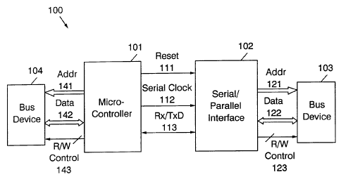
FIGURE 1 illustrates a block diagram of an embodiment of a microcontroller
system
using the present invention;
FIGURE 2 illustrates a block diagram of an embodiment of the seriallparallel
interface of the present invention;
FIGURE 3 illustrates a block diagram detailing another embodiment of the
seriallparallel interface of the present invention;
FIGURE 4 illustrates a flow diagram of the row, column/count state machine of
FIGURE 3; and
FIGURE 5 illustrates a flow diagram of the readlwrite state machine of FIGURE
3.
DETAILED DESCRIPTION
In the following description, numerous specific details are set forth to
provide a
thorough understanding of the present invention. However, it will be obvious
to those
skilled in the art that the present invention may be practiced without such
specific details.
In other instances, well-known circuits have been shown in block diagram form
in order not
to obscure the present invention in unnecessary detail. For the most part,
details
concerning timing considerations and the like have been omitted inasmuch as
such details
CA 02231362 1998-03-09
AT9-97-210
are not necessary to obtain a complete understanding of the present invention
and are
within the skills of persons of ordinary skill in the relevant art. During the
following
description of the implementation of the present invention, the terms "assert"
and "negate"
and various grammatical forms thereof, are used to avoid confusion when
dealing with a
mixture of "active high" and "active low" logic signals. "Assert" is used to
refer to the
rendering of a logic signal or register bit into its active, or logically
true, state. "Negate" is
used to refer to the rendering of a logic signal or register bit into its
inactive, or logically
false state.
Refer now to the drawings wherein depicted elements are not necessarily shown
to scale and wherein like or similar elements are designated by the same
reference
numeral through the several views.
An invention that alleviates the pinout problem in a microcontroller system,
and
incorporates dynamic updating of the operating software will now be described
in detail.
Referring to FIGURE 1, there is shown a microcontroller system 100 in
accordance with
one embodiment of the present invention. Microcontroller 101 communicates with
the
seriallparallel interface 102 by means of three signal lines, Reset 111,
Serial clock 112,
and Rx/TxD 113. An operation which might either download data to a parallel
bus device
103 or upload data from the parallel bus device 103 is initiated by a signal
on reset line
111. Serial data is either clocked out of microcontroller 101 serial port or
into
microcontroller 101 serial port depending on the operation. Serial data is
communicated
between the bidirectional serial port of microcontroller 101 and the
seriallparallel interface
102 on the bidirectional serial data line, RxITxD line 113. The serial clock
of
microcontroller 101 is sent to serial/parallel interface 102 via serial clock
line 112. In a
download, or write, operation, serial data is received by the serial/parallel
interface 102,
and provided to parallel bidirectional data bus 122. Data bus 122 is an m-bit
parallel data
line, where m is a predetermined integer number of bits. Conversely, in an
upload, or read,
operation, bus device 103 sets up the data to be sent to microcontroller 101
on the
bidirectional data bus 122 where it is received by the seriallparallel
interface 102. Data is
then clocked out by the seriallparallel interface 102 on line RxITxD 113 where
it is received
CA 02231362 1998-03-09
AT9-97-210
at the serial port of microcontroller 101. The address at which data is either
to be written
or read is provided to seriallparallel interface 102 on its address line 121.
Address line 121
is an n-bit address bus, where n is a predetermined integer number of bits.
Seriallparallel
interface 102 informs bus device 103 when a read or write operation is being
executed
using readlwrite ("RIW") control bus 123. Seriallparallel interface 102 may
access more
than one bus device. In such an embodiment, RIW control bus 123 would
implement a
chip select signal on one of its lines. Chip select operation and circuitry
are understood
by artisans of ordinary skill in the art. Bus device 103 may be implemented as
a memory,
including nonvolatile memory, or a peripheral bus device in one embodiment of
the
invention. Additionally, it should be noted that bus device 103 may be any
device in a data
processing system that communicates via a parallel bus.
Microcontroller system 100 may also include other bus devices such as bus
device
104 which reside in the address space of microcontroller 101. Data is
transmitted to, or
received from, bus device 104 on parallel data bus 142, and the address at
which the read
or write operation takes place is provided by an address bus 141 of
microcontroller 101.
Microcontroller 101 informs bus device 104 as to a read or write operation by
asserting
read/write bus 143. A more detailed understanding of the invention may be had
by now
referring to FIGURE 2 depicting a block diagram of an embodiment of
seriallparallel
interface 102.
An operation is initialized by microcontroller 101 (not shown in FIGURE 2)
asserting
reset line 111. In response to the signal on reset line 111, control logic 207
resets address
logic 203 and clock sequencing logic 201 by asserting the interface reset line
272.
Microcontroller 101 then clocks out the initial n-bit address to be asserted
on address line
121. The initial n-bit address corresponds to the location of the first block
of data to be
uploaded or downloaded. This address is clocked into shift register 202 by
register clock
211 generated by clock sequencing logic 201. Clock sequencing logic 201
receives the
serial clock from microcontroller 101 on serial clock 112. Register clock 211
is
synchronized with serial clock 112. Microcontroller 101 may send the initial
address
byte-by-byte. In such an embodiment, microcontroller 101 sends bytes of the
address
CA 02231362 2001-08-24
AT9-97-210
sequentially until all n-bits of the address have been sent. Clock sequencing
logic 201
accumulates serial clock cycles. After all n-bits are received, clock
sequencing logic 201
latches the address which appears on the parallel bus 221 of shift register
202 into address
logic 203 by asserting address latch 212. Parallel bus 221 is Z bits in
length, where Z is
predetermined integer value.
Afterthe initial address has been transmitted, microcontroller 101 sends a
command
byte. Control logic 207 receives the serial clock from microcontroller 101 on
serial clock
line 112. It accumulates clock cycles until the eight bits of the command byte
have been
clocked in. It then latches the command byte which it receives on the parallel
bus 221 of
shift register 202. The state of the first bit of the command byte determines
whether the
operation to be performed is a read or a write. The control logic 207 then
uses this to
establish the state of R/W enable 271. Input data buffer 205 and output data
buffer 206
are enabled or disabled according to the state of R/W enable line 271.
Read operation commences when microcontroller 101 issues a read command to
its serial port. The serial clock signal 112 is passed to the output data
buffer 206 by clock
sequencing logic 201 via data clock line 213. Output data buffer 206 has been
enabled
by the signal on the R/W enable line 271. A read state is also asserted on R/W
control bus
123 informing the bus device 103 that a read is being performed. The m-bits of
data are
serially read out, then control logic 207 asserts the address count increment
signal 273,
causing address logic 203 to address the next m-bit data block. After m-bits
of data have
been provided to microcontroller 101, clock sequencing logic 201 stops issuing
clock
signals to output data buffer 206. M-bit blocks of data are sequentially
received by
microcontroller 101 by repeating this operation. The read operation is
terminated when
microcontroller 101 asserts reset 111, to indicate that serial/parallel
interface 102 should
be reset in anticipation of the next operation.
Write operation commences when microcontroller 101 writes data to its serial
port
in response to an instruction in the software code. This is not shown herein,
but it is well
understood by one of ordinary skill in the art. Input data buffer 205 receives
the m-bit data
block on the parallel bus 221 of shift register 202. The data are latched into
input data
CA 02231362 1998-03-09
AT9-97-210
buffer 205 in response to data clock 213. Control logic 207 may control the
latching of
data into input data buffer 205 via input data buffer control line 274. In an
alternative
embodiment, alternative means may be used to latch data into input data buffer
205. Such
means are well know in the art. Control logic 207 also receives data clock
213. In
response thereto, control logic 207 asserts a write state on RIW control bus
123, causing
bus device 103 to access the data on the data bus 122. Control logic 207 also
asserts
address count increment 273, causing address logic 203 to increment an address
counter.
The address of the location into which the next n-bit block of data is to be
downloaded is
then provided on address bus 121 by address logic 203. The write operation
continues to
execute these steps until all of the data to be downloaded has been
transmitted.
Microcontroller 101 then signals the end of the write operation by asserting
reset line 111,
to inform the seriallparallel interface 102 to reset in anticipation of a next
operation.
Data may be downloaded byte-by-byte in an interleaved fashion. In such an
embodiment, if a write operation has been contemplated, the last four bits of
the command
byte contain the lower four bits ("low nibble") of the first output byte. If a
read operation is
contemplated, the value of bits one through seven of the command byte are
ignored.
Control logic 207 decodes the first bit of the command byte, and on detecting
the write
operation, instructs input data buffer 205 to latch these four bits. Control
logic 207
decodes the first bit of the command byte, and on detecting the write
operation, instructs
input data buffer 205 to latch these four bits. Then, the low nibble of the
first output byte
sent by microcontroller 101 contains the upper four bits ("high nibble") of
the first data byte,
and the high nibble of the first output byte contains the low nibble of the
next data byte to
be downloaded. Control logic 207 steers the latching of the output byte into
internal
registers (not shown) in input data buffer 205, via input buffer control bus
274. This
steering effects the assembly of the two nibbles, transmitted in interleaved
fashion, into a
full data byte. It would be well understood by an artisan of ordinary skill
that
communication of data bytes using this method is independent of whether the
mode of
data representation is least significant bit ("LSB") first, or most
significant bit ("MSB") first.
Control logic 207 continues to accumulate input data byte-by-byte until all m-
bits of data
CA 02231362 1998-03-09
AT9-97-210
have been assembled. It then loads the data into input data buffer 205 and
operation
continues as described above. Further understanding of the operation of the
invention
may be had by now referring to FIGURE 3 in which a block diagram of another
embodiment of the invention is shown.
In FIGURE 3, operation begins with microcontroller 101 (not shown in FIGURE 3)
asserting reset 111 to causes readlwrite state machine 307, row, column-count
state
machine 308, and command logic 309 to reset. Microcontroller 101 then
commences to
download an initial address on address bus 121 at which a download or upload
operation
is to begin. Microcontroller 101 transmits the n-bit address by clocking the
address out of
its serial port on RxITxD line 113. The address is clocked into shift register
202 on
serial/parallel interface 102; the address transfer may be byte-by-byte.
Microcontroller 101
also outputs its serial clock on serial clock line 112. Clock generator 301
receives serial
clock 112 and outputs interface serial clock pulses on interface clock line
311. The
interface clock is synchronized to serial clock 112. Clock generator 301 may
output an
interface clock pulse on each of the rising and falling edges of serial clock
112. Clocking
of shift register 202 is controlled by the signal on interface clock line 311.
The initial address is stored by a plurality X of mutiplexers-with-latch
referred to as
304-0 through 304-X, where X is an integer value equal to a predetermined
number of
multiplexers-with-latch. The initial address may be stored byte-by-byte.
Mutiplexer-with-latch 304-1 through mutiplexer-with-latch 304-X are coupled to
the parallel
bus 321 of shift register 302. A mutiplexer-with-latch that will store the
current block of the
m-bit address being transmitted is selected by decoding the row and column
count signal
provided on output bus 381 of row, column-count state machine 308. A block of
the n-bit
address may be a byte in length. After the current block has been clocked out
of
microcontroller 101 and into shift register 202, the address is latched into
the selected one
of mutiplexer-with-latch 304-0 through mutiplexer-with-latch 304-X by an
interface clock
pulse on line 311. After all n-bits of the address have been sent, the address
is loaded into
address counter 303.
CA 02231362 1998-03-09
AT9-97-210 ~ o
Row and column select signals are generated by row, column-count state machine
308. Row, column-count state machine 308 receives interface clock pulses from
clock
generator 301 on interface clock line 311. A flow chart of an embodiment of a
row,
column-count state machine 308 is illustrated in FIGURE 4.
After reset, row, column-count state machine 308 accumulates interface serial
clock
pulses received on interface serial clock line 311. The logic to accumulate
clock pulses
is internal to row, column-count state machine 308 and is not shown in detail.
If the
number of clock pulses accumulated has not reached Y, the row, column-count
state
machine 308 increments the column count, outputs the row and column-count and
continues to interface serial clock cycles recf:ived on interface serial clock
line 311. Y is a
preselected integer corresponding to the length of a data block to be
downloaded in a
single download cycle. Furthermore, in an embodiment in which all m bits of
data are
downloaded on one cycle, Y would equal m. An embodiment downloading byte-byte
would
have a value of Y equal to eight. Moreover, in the present invention, after
microcontroller
101 first sends an n-bit address, row, column-count state machine 308 may
adaptively set
Y. For example, in an embodiment where the entire address is sent as a block,
Y is initially
set equal to n. After the n-bits have been received, row, column-count state
machine 308
may set Y to a new preselected value. This new preselected value would be m in
an
embodiment in which m data bits are to be downloaded in a block. In an
embodiment in
which both the n-bit address and the m-bit data are sent byte-by-byte, Y would
have a fixed
value of eight.
If the clock accumulator has reached Y, the row, column-count state machine
308
increments the row count, resets the column count, and outputs the row and
column count
on its output bus 381. If a reset has not been received from microcontroller
101 on reset
line 111, the row, column-count state machine 308 continues to accumulate
clock cycles
and continues to increment the row and column-counts as previously described.
If a reset
has been received on reset line 111, then the row, column-count state machine
308 resets.
When the next operation commences, row, column-count state machine 308 begins
accumulating clock cycles as they are received. The timing of the sequential
operation of
CA 02231362 1998-03-09
AT9-97-210
row, column-count state machine 308 is controlled by its internal clock (not
shown). The
internal clock need not be synchronized with the interface serial clock pulses
on line 311,
and the rate of the internal clock may be much greater than the rate of the
interface serial
clock pulses on line 311.
After sending the n-bit initial address, microcontroller 101 sends a command
byte.
Command logic 309 decodes a row and column address received from row, column-
count
state machine 308 on output line 381. After the eight bits of the command byte
have been
clocked into shift register 302, command logic 309 latches the command byte
which it
receives on the parallel bus 321 of shift register 302. The state of the first
bit of the
command byte informs the seriallparallel interface 102 whether the operation
to be
performed is a read or a write. Command logic 309 ascertains the state of the
first bit of
the command byte and sets the state of read/write state machine 307 through
output line
391 of command logic 309. In one embodiment of the present invention in which
data
transfer is byte-by-byte, if a write operation is to be performed, the last
four bits of the
command byte includes the lowest nibble of the first data byte to be
downloaded, as
describe above.
Read and write operations are controlled by readlwrite state machine 307. A
flow
chart of an embodiment of a readlwrite state machine 307 is illustrated in
FIGURE 5.
Readlwrite state machine 307 receives the output row and column addresses on
the row
and column address bus 381 by the row, column-count state machine 308. If the
command logic has been addressed, then readlwrite state machine 307 tests the
state of
the output line 391 of command logic 309. If line 391 is in a read state,
readlwrite state
machine 307 asserts a read on RIV1I control bus 123. It then commands read
data buffer
206 to latch the data on data bus 122 via line 371. The first block of data to
be sent
resides at the initial address loaded into address counter 303. If, after m-
bits have been
sent, a reset has not been asserted, RIW state machine 307 increments address
counter
303 so that the address of the next block of data to be read appears on
address bus 121.
Address counter 303 increments the address on address bus 121 in response to
the
address increment signal received from readlwrite state machine 307 via
address counter
CA 02231362 1998-03-09
AT9-97-210
increment line 372. After latching the data, read data buffer 206 clocks the
data out via
serial data line RxITxD 113. Clocking of the data is controlled by the serial
clock pulses
asserted by clock generator 301 on interface serial clock line 311. After the
address
counter 303 has been incremented, the cycle repeats until a reset is asserted
on reset line
111 by microcontroller 101 (not shown).
If a write is to be performed, readlwrite state machine 307 accumulates the
number
of bits received. When m-bits have been received, read/write state machine 307
asserts
a write on RIVII control bus 123. Read/write state machine 307 then tests to
see if a reset
has been asserted. If a reset has been asserted, readlwrite state machine 307
resets,
otherwise, it increments address counter 303 via address counter increment
line 372. This
cycle repeats until a reset has been asserted on reset line 111 by
microcontroller 101. The
timing of the sequential operations of RIW state machine 307 is controlled by
its internal
clock (not shown). The internal clock may not be synchronized with the
interface serial
clock on line 311, and the rate of the internal clock may be much greater than
the rate of
the interface serial clock pulses on line 311..
In a write operation, data to be written to data byte 122 is received by data
logic
305. Data may be transmitted from microcontroller 101 byte-by-byte. In such an
embodiment the command byte includes the lowest nibble of the first data byte
to be
downloaded, as discussed above. Data lagic 305 receives the command byte on
the
parallel bus 321 of shift register 202. The next byte sent by microcontroller
101 through
its serial port, RxITxD 113, contains the high nibble of the first data byte
in its lower four
bits, and the low nibble of the next data byte in its four upper bits. Data
logic 305 receives
the next byte transmitted by the parallel bus 321 of shift register 302 and
latches this
output byte. Data logic 305 then concatenates the low nibble and the high
nibble of the
first data byte and transfers it to data bus 122. Microcontroller 101
continues to transmit
data on serial line RxITxD 113 in this interleaved fashion. Data logic 305
latches the
output bytes as they are received and concatenates the low nibble and high
nibble of each
byte of data as described above. Latching of the data at data logic 305 is
controlled by the
interface serial clock pulses generated on line 311. It would be well
understood by an
CA 02231362 1998-03-09
AT9-97-210
artisan of ordinary skill that communication of data bytes using this method
is independent
of whether the mode of data representation is LSB first, or MSB first. After m-
bits of data
have been transmitted, the data is written to bus device 103 by readlwrite
state machine
307 asserting a write state on R/W control bus 123. If, after m-bits have been
sent, a
reset has not been asserted, RIW state machine 307 increments address counter
303 so
that the address of the next block of data to be read appears on address bus
121. Address
counter 303 increments the address on address bus 121 in response to the
address
increment signal received from readlwrite state machine 307 via address
counter
increment line 372. Subsequent m-bit blocks of data are transmitted in this
way until all the
data to be downloaded has been sent, and microcontroller 101 asserts a reset
on reset line
111. Seriallparallel interface 102 is then ready to begin the next operation.
The data processing system and methodology represented in the embodiments
described herein are effective solutions to the associated problems of
interfacing bus
devices with an embedded controller having a limited number of parallel I/O
buses, and
dynamic updating of the operating software of the data processing system.
Although the
present invention and its advantages have been described in detail, it should
be
understood that various changes, substitutions and alterations can be made
herein without
departing from the spirit and scope of the invention as defined by the
appended claims.