Note: Descriptions are shown in the official language in which they were submitted.
CA 02231396 1998-03-09
W O 97/13302 PCT/~5G~2~75
- 1 -
Optically Rescsllallt S~ructure
Field of the Invention
This invention relates to an optically resonant structure and has particular but5 not c~lus;ve application to a vertical cavity surface ~mirting laser (VCSEL).
Background
In a conventional Fabry Perot diode semiconductor laser, a resonant cavity is
formed f~Yren~ling longin~lin~lly in the plane of the semiconductor substrate
o with reflective structures at opposite ends. In contrast, in a VCSEL, the
resonant cavity is arranged vertically in the substrate with the advantage that
light is ~r~ perpen~ rly from its surface over a larger area than
with a horizontal structure, which renders the VCSEL well suited to
l~nlnrhing signals into optical teleco.. ~ tions fibres. An example of a
15 VCSEL is given in IEl-E Photonics Technology Letters Vol. 7 No. 6 June
1995 pp 608-610, M. A. Fisher et al. The device ror~cictc of a semiconductor
substrate on which are formed first and second reflective means that comprise
periodic Bragg reflective structures, with a resonant cavity be.w~ them that
inrh~ c a layer of laser active material with spacer layers to provide a
20 sllffiri~ont cavity thirknrcc to achieve resonance at a desired operating
w~dength ~. The first reflective means may comprise a plurality of
- interleaved layers of different semiconductor materials with different rcLa. ~ivc
indices of ~/4 cLrc~L;ve thirkn~occ~ ovc.lyiilg the substrate. The Bragg
structure of the second reflective means overlies the Cdvity and is formed of
25 layers of dielectric material, with different lcLd~Livc in~lices, of )~/4 eLL~Livc
thirkn~ss
In order to pass current through the laser active m~teri~l in the cavity, a
metal contact is formed on the underside of the substrate and a conductive
30 contact layer is formed between the dielectric second reflective means and the
layers in the resonant cavity. Current is confined to the cavity by a
peripheral reverse-biassed junction.
CA 0223l396 l998-03-09
W O 97/13302 PCT/GB96/02375
-2-
The thirlcn~cs of the reso~nt cavity is typically of the order of 1 ~m, whereas
in a plane perpenr~ ar to the thirkn~cc, the cavity has a relatively large
av~ae ~imrncion; the cavity is typically square or circular when viewed
from above with a rli~m~ter or side length of the order of 5~ 20 ~m.
A problem that arises in conventional VCSEL structures is that during
resonance of the cavity, the transverse mode of resonance is left largely
uncontrolled and the relatively large ~ mloter of the cavity may support a
number of dirr~re.lt Ll~la~ae modes, which leads to mode co~ ion and
~o instability.
Use of a surface grating of concentric circular ~l~mlonrs in a conventional
distributed feerlha~k ( DFB) or distributed Bragg reflector (DBR) laser, with a
horizontal, rather than vertical resonant cavity is rlic~losecl in "Circularly
15 Symmetric Operation of a Concentric-Cirde-Grating, Surface-F.I.;~ g,
AlGaAs/GaAs Q.,~ ..-Well Semiconductor Laser", T. Erdogan et al, Appl.
Phys. lett. 60 (16) 20 April 1992 pp 1921-23. With this device, a coll~,cn~ionaltransversely ~ n-ling resonant cavity is provided with a surface grating
which produces surface emission from the laser by second order Bragg
20 reflection. The circular pattern of the grating resuks in the emission of a
circularly ayl~ e~l;c bearn.
Another device is described in US Patent No. 5 301 201 and "Zone Laser"
Appl. Phys. Lett. 65 (2) 11 July 1994 pp 144-146, D. Vakhshoori et al, in
.75 which the laser cavity is divided into a plurality of conoentric zones which each support an individual resonant mode. The outputs of the concentric
zones sum together in a similar way to light from the zones of a Fresnel lens,
thereby focusing the laser output into a single spot.
30 In Applied Physics Letters, Vol 66, No. 21, 22 May 1995, pp 2769-2771, J. H.
Ser et al, there is described a VCSEL which has an overlaid fine metal
interlaced grating etched on its upper DBR, overlying its light emitting face.
CA 02231396 1998-03-09
W O 97113302 PCT/GB96/02375
The p~l~oSc of the grating is to produce polarisation stabilisation, for exampleto select TM polarisation as the dominant polarisation mode.
S~ of the Invention
5 The pre ent invention offers an alternative approach. In accordance with the
invention, there is provided an optically resonant structure coll~l;sing first
and second reflective means spaced apart so as to provide an optically resonant
cavity with a l~ldL;v~ly small thi~knPss ~im.onqion between the reflective
means and e~t~n~ing over an area with rcldLivcly large L~allsvclac f~imPnqions
o in a plane transverse to the thickness ~imPncion, and means for rPflPcting a
component of the opl;ical radiation from the cavity travelling parallel to said
plane, with a phase characteristic for supporting a prPqPlPcte~l tr~lav~ae
resonant mode in the cavity.
s The reflective means may comprise means for pro~ll~ing Bragg reflection of
radiation from the cavity. The Bragg reflection may be produced by means of
a pattern of material with a spatially periodic optical refractive index
~a~d~Lc~ ;S~iC.
20 The structure accolLllg to the invention may be used in a laser, for example a
VCSEL, so that a layer of laser active material for producing optical radiation
may be provided between the first and second reflective means. The layer of
laser active m~tPri~l may be spaced from the reflective means by at least one
spacer layer.
The invention also inc~lllrlPs an optically resonant structure comprising means
for providing an optically resonant cavity, optically active material with a
rcldLivcly small thic kness ~im~nqion and P~rten~ing over an area with relatively
large L~allav~lac rlimlonqionâ in a plane transverse to the thi~kn~qc rlimPnqi~n~
30 wherein means are disposed around the active material for rloflPcting a
component of the optical radiation therein travelling in said plane with a
phase characteristic for supporting a prffPlP~e~ transverse resonant mode in
-
CA 02231396 1998-03-09
WO 97/13302 PCT/GB96/02375
the cavity.
The means for producing Bragg reflection may comprise 5 pattern of rings
formed in at least one of the layers of the structure. In the embodiment
5 described herein&er, the rings are formed in a blocking layer, which confines
current flow through the cavity.
The rings may be of different widths in order to m~~imice support of the
prPcPlpcterl reson~nt mode for the cavity. The rings may comprise grooves
10 formed in the layer or alternatively ridges which are llpst~n~ing from the
layer.
So-called Bragg w~v~uides have been proposed previously in which
co~ ional waveguide ~ ing is replaced by a periodic multilayer structure
15 with high refle~ Livi-y that results from interference between partial reflections
at a number of the inr~rf-~Ps between the layers. Bragg w-dv~,uides,
inrln~ing antireso~-~nt rpfl~octing optical w~Lv~,uides or ARROWs were
proposed and first demonstrated in GaAs planar structures in 1977, see P.
Yeh, A. Yariv, C-S Hong, J. Opt. Soc. Am. 67, 423 (1977) and A. Y. Cho,
20 A. Yariv, P. Yeh, Appl. Phys. Lett. 30, 471 (1977). The idea was P~enr~ecl toa cylindrical geom~orry but the benefits in respect of a conventional cylindrical
wd~.~,uide were found to be unreaiisable in practice for optical fibres because
the fabrication tolerances are unrealistic and the l~lln~hing of light is
in~ ient see N. J. Doran K. J. Blow, IEEE J. Light. Tech. LT-1, 108 (1983).
25 It has however been found in accordance with the invention that a periodic
Bragg reflector arr~nglompnt around the cavity of a VCSEL can support a
plc3rlP~ resonant mode in the cavity of the laser, without suLr~,;ng from
the previously ~liccllcse~ disadvantages which occur in respect of an optical
fibre.
Brief Dw~ ion of the Drawings
In order that the invention may be more fully understood, an embodiment of
CA 02231396 1998-03-09
W O 97/13302 PCT/GB96/02375
a VCSEL with a cylindrical Bragg waveguide, will now be described by way
of exarnple with reference to the accol~lp~lying drawings, in which:
Figure 1 is a 5rh~m~rir sectional view of a VCSEL with a circular Bragg
structure surrounding its cavity according to a first emborlim~nt of the
.
5 lnVentlOn;
Figure 2 is a top plan view of the cavity shown in Figure l;
Figure 3 is a graph illustrating the field amplitude as the function of radial
~ict~nr~ from the centre of the cavity shown in Figure 2, together with the
spatial periodic refractive index variation of the Bragg structure in the radial10 direction; and
Figure 4 is a sectional view corresponding to Figure 1, of a second
embodiment of a device according to the invention.
Detailed Dcs~ Lio~
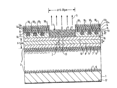
15 The basic VCSEL structure shown in Pigure 1 is generally sirnilar to that
described by Fisher et al supra and colll~l;ses a s~omi~onrll.rtQr substrate 1 of
InP material on which a resonant cavity 2 is formed, of thirkn~cs X bc.w.ell a
first reflective means 3 and a second reflective means 4. The ~limrncit~ns of
the cavity are so arranged that in use, light of a pr~ pt~rminr~ wavf-len~:h
20 e.g. 1.55 ~Lm is generated by laser action and emittecl in the direction of
arrows 5.
The first reflective m~eans 3 is electrically conductive and comprises a plurality
of interleaved layers of InGaAsP 6 of bandgap equivalent wdvle~ h 1.4
25 microns, and InP 7 of ~/4 tLr~ive thirkn~sc that are deposited on the
substrate as a stack with 45 periods, so to provide a 90 layer DBR structure.
The layers 6, 7 are typically deposited by conventional gas source MBE
techniques.
30 In the resonant cavity 2, an undoped InGaAsP laser active material layer 8 ofbandgap equivalent wavelength of 1.55 microns of a thi~knrs~ corresponding
to one w~k.l~,~h al: 1.55 ,um (i.e 0.45 - 0.47 ~Lm) is ~ wn onto the first
-
CA 02231396 1998-03-09
W O 97/13302 PCT/GB96/02375
reflective means 3 by atmospheric pressure metalorganic vapour phase ~;L~ULY
(MOVPE) between an n-doped layer of InP 9 which acts as a underlying
spacer layer, and an overlying spacer layer 10 formed of p-doped InP material.
The thirkn~cc~oc of the spacer layers 9,10 are s~l.octe~ so that the cavity
s produces resonance at the desired operating wavelength of )~ ; 1.55 ~m (i.e.
with the overall cavity rlim~nci~n X being around 1~m).
The second reflective means 4 COlllpr;SeS an interleaved stack of ~ nc
material corlcicting of layers 11 of Al203 material interleaved with layers 12 of
o Si material, the layers being deposited by conventional evaporation technigues.
The layen 11, 12 have an err~ivc wav~l~ngrh thirkn~ss of ~/4 and are of
different lcr.d~L;vc indices so as to act as a DBR in a similar m~nn~or to the
fint reflective means 3, although the layen 11, 12 are electrically non-
con~ cting
In order to energise the laser, an elecrric current is passed LLl~ou~;ll ther~;oll~ cavity 2, from an ~l~ctrir~lly conductive p-doped GaInAsP contact
layer 13 of ~-n~lg~p equivalent w.L~ ngth 1.4 microns on the undenide of
the dielectric reflector 4, the layer 13 being conn~cte~ to a metal contact layer
20 14 formed by vapour deposition on an interm~ te contact layer 15 formed
of p~ GaInAs material, deposited on the layer 13. An external electrical
conn~ction, not shown, is provided to the layen 13, 14. A current blorking
layer 16 formed of n-doped InP material is deposited on the upper spacer layer
10 and, by conventional photolithography and et~hing, as for the structure
25 described by Fisher et al s~pra, a central aperture D of ~ m~t~r d, typically of
the order of 5-20 ~m, is formed, which defines the active region for the cavity.It can thus be seen that the cavity of the VCSEL has a relatively small
vertical thirknPcs ~im~ncion X between the first and second reflective means
3, 4 and a l. ldLiv~ly large ~r~lav~ae ~impncion d in a horizontal plane,
30 hdhSv~,~aC to the thi~kn~os5 rlim~ncinn. Likewise, the thi~kn~oss ~im~ncion ~ of
the active layer 8 is small in comparison with the transverse ~lim~oncion The
~lim~oncion ~ is typically of the range of 0.45-.47~m and the ~lim~onciorl X is in
CA 0223l396 l998-03-09
W O 97/13302 PCT/G~6/~2375
the region of 1~m. This is in contrast to a conventio~l edge ~mitting laser
which P~Pn~ls lon~inl~in~lly in the plane of the substrate, for which a typical
length is in the range of 300 to 500 ~m, or greater. It will be seen that the
electrical contact layer 13 forms direct electrical contact with the spacer layer
5 10 in the central aper~ure D so that current passes through the materials in the
cavity, in this region. The current can pass through the semiconductor
materials that form the first reflective means 3, and the substrate 1 so as to
reach a Au metal conract 17 on the underside of the substrate. However, the
blocking layer 16, produces a reverse p-n junction with the p-doped spacer
10 layer 10 so as to confine current flow through the central apercure D. Thus,
the current passes through the layer 8 in this active region to generate opticalradiation which resonates in the cavity 2. It will be understood that due to
the distributed nature of the multi-layer first and second reflective means 3, 4,
the optical path length over which light resonates between them has an
15 average length which is greater than the physical ~limPnci~n X shown in
Figure 1.
In accordance with the invention, a series of circular rings 18 is formed in theU~ loSt surface of the blocking layer 16. As shown in Figure 2, six rings
20 18l-186 or more may be pr~re~l~l although, in Figure 1, only four rings are
shown for ease of illustration. As shown in the drawings, the central region
D has a circular periphery and rings 18 are concentric with the circular centralregion. In the embor3imPnt shown in Figure 1, the rings are formed as
~pst~nrling ridges from the general planar extent of the blocking layer 16.
25 This is achieved during m~mlf~lre, prior to the deposition of the layers 11
to 15, by electron beam lithography and sclc~;ve etching of the blocking
layer 16. Initially, the layer 16 is laid down with a CQ~ clOus thi~kn~cc y
ant is subsequently etched selectively by an amount z so as to define the
ridges 18. In an altc.l.dLiv~ embodiment (not shown), grooves can be etched
30 into the blo~king layer. The electrical contact layers 13, 14 and 15 fill thespaces between the rings 18 when subsequently deposited on the layer 16.
CA 02231396 1998-03-09
W O 97/13302 PCT/GB96/02375
The n-doped InP material of the layer 16 has a dirrc~ L optical refractive
index from the materials that form the electrode layers 13, 14 and 15, so that
the rings 18 form a reflective Bragg structure for light from the cavity 2
which, whilst travelling in the direction o~ arrows 5 has a component in a
plane parallel to the plane of the optically active layer 8. The rings 18 and
the illL~ ; material of layers 13, 14, 15 produce a spatially periodic
refractive index pattern which confines the component travelling parallel to
the aforesaid plane to the centre of the circular region D. Figure 3 shows the
spatially periodic pattern is sPlPcrecl so that the phase of the r~Pcte-3 light
10 constructively supports a presel~ctefl r~so~nr mode for tke resonant cavity 2.
Typically, the mode comprises the HE1l mode which has a field amplitude as
a function of radial ~lict~n~e outwardly from the centre O of the central
region D, as shown in Figure 3. The field arnplitute has a s~ lly
i:~n peak at the centre O and tecays towards the outer edge of the
~s central region D. The spatially periodic refractive index pattern forrned by
the ridges 18~-18~ is shown in Figure 3 as a function of radial ~ict~n~e r, for a
sitl~-tior~ where the central region D has a ~i~m~t~~r d of 9.2 ~m (r = 4.6 ~m).
The radial width of the ridges 18 may change from ridge to ridge.
20 Furthermore, the spacing between the ridges may differ. The specific ridge
configuration is chosen to support the pr.osPlPr~e~ resonant mode for the
resonant cavity 2. In one example, the innermost ridge 18l was wider than
the other ridges. The actual width may be computed according to the
principles set out by Doran et al, s~pra.
Alternating layers lla of A1203 and 12a of Si are formed over the rings 18.
The ~ltPrn~ting layers lla, 12a form a DBR for r~flPcting the optical field thatoccurs outside the central region D.
30 Without the provision of the ridges 18, the HEll mode has to compete with
other modes and thus tends to be unstable, but the provision of the Bragg
structure provided by the rings 18 perrnits stabilisation of the prPselP~e~
CA 02231396 1998-03-09
W O 97/13302 PCT/Gn9GI'~2375
transverse mode.
Another configuration of the structure is shown in Figure 4, and can be
corlci~le.et as a modifir~tion of the device structure shown in Figure 1. Like
parts are marked witk the sarne reference numbers. In the embodiment of
Figure 4, the blocking layer Colllpliscs a layer 19 of semi-inc~ ting InP which
is selectively re-grown around the cavity.
In order to form the structure, the active and spacer layers 8, 9, 10 are formedlO on the first reflective stack 3 as described with re~erence ~o Figure 1, an
then a mesa of ~ d, corresponding to the previously described area D
for light emission, is formed from layers 8, 9, 10, by conventional lithography
and etrhing A planar, semi-inclll~tin~ layer 19 of InP is then re-grown all
around the mesa. A suitable technique for the re-growth that uses PCl3 haâ
been described in a paper by M. J. Harlow, P. C. Spurdens and R.H. Moss:
"The inflll~n~e of PCl3 on the planarisation and sclc~iv;-y of InP re-growth
by atmospheric ~c~a~ MOVPEn, Proceerling.c of the 7th Tntern~tional
Convention on Tnrlitlm Phosphide and Related Materials, 9-13 May 1995,
Sapporo, Japan. The semi-inclll~ting InP layer 19 was iron doped to provide
20 Cle~,Lro~ traps in the layer, but it will be appreciated that other suitable
dopants could be used. The regrown layer 19 has the advantage of providing
a flat surface that is contiguous with the upper surface of the spacer layer 10,that can receive the various layers of the reflector structure 4, so that the step
in the reflector shown in Figure 1 around the edge of the region D, is avoided
25 in the structure of Figure 2. Reference is also directed to "Very Rapid and
Selc~ l.ivc Epitaxy of InP around Mesas of height up to 14~m by Hydride
Vapour Phase Epitaxy" S. Lourdudoss et al Conference Paper IPRM '94.
.
The confining Bragg structure 18 is then etched in the top of the layer 19 in
30 the manner described previously with reference to Figure 1. The cont?cring
layers 13, 15 are then formed over the entire top surface, whereas the mPt~llic
contact layer 14 is forrned only on the surface that lies outside of the area D
CA 02231396 1998-03-09
W O 97/13302 PCT/GB96/02375
- 10 -
where light is e ..;. ~ The second reflective means 4 is then formed over the
top surface, as previously described, and a suitable electrical connPction is
made to the layer 14, not shown, in order to provide an P~rPrn~l connPction,
e.g. by lor~ e-l etching and mPt~llicqtion or other conventional techniques.
s
Mo~lifir~tions and variations of the described structures are possible. For
example, the spaces between the ridges 18 need not n~e~.;ly be filled with
material and could be left empty. Alternatively, the spaces between the ridges
could be filled with a ~irL~en- material, for example polyimide material.
~o Also, the ridges 18 could be made in other layers of the structure, for
example, in either of the underlying spacer layers 9, 10.
Furthermore, the invention is not n~c~ss~.;ly restricted to lasers and it will be
appreciated that the cavity 2 could be used as a passive cavity, without the
15 need for P~ecrr1c~l contacts, for example, to be used as an all optical switch or
bistable r~ l Passive cavities are well known per se in the li~C-d~UlC of
microresonators, and have application in all-optical switrl~ing, logic,
bistability, etc, see for example the paper "GaAs-AlAs Monolithic
Microresonator Arrays" J.L. Jewel, A Scherer, S.L. McCall, A.C. Gossard &
20 J.H. Fngli~h, Appl Phys Lett, Vol 51, No 2, pp 9~96 (1987). The transverse
mode confinPmPnt produced by the present invention ,~e~ an advance
over the use of pillar structures as described in this reference, in terms of
5S
25 In another mt-rlifir~ri~n, the rings 18 and the central region D are made
elliptical in order to impart a predetermined polarisation to the emirterl lightfor example with an ellipticity of 10-30%.
The invention is also applicable to a VCSEL in which the reflective layers 11,
30 12 are replaced by an anti-reflection stack, and the second reflective means
co~ .;.es a mirror ~rPrn~l to the semiconductor substrate, and reference is
directed to "A C.W. P~rtPrn~l cavity surface emitting laser~ by J. V. S~n.lll~ky
CA 02231396 1998-03-09
W O 97/13302 PCT/GB96/02375
A. Mukherjee and S.R. Brueck paper TuEll at the Conference on
Semiconductor lasers: Advanced Devices and Applications (Keystone,
Colorado, August 21-23, 1995) - Optical Society of America 1995 Terhn
Digest Series, Volume 20, pp 153-155.