Note: Descriptions are shown in the official language in which they were submitted.
CA 02231~73 1998-03-10
W O 97/12414 PCTAJS96/15144
BATTERY PACK HAVING A DISCONNECT SWITCH CIRCUIT
Technical Field
This invention relates in general to battery packs, and in particular to
5 battery packs having self actuating disconnect switches.
Background of the Invention
The safety of portable energy storage systems, such as rechargeable
battery packs, is a primary concern among reputable manufacturers. A
1 0 significant portion of the cost of a typical battery pack results from the
inclusion of safety mechanisms. One such safety mechanism is a polyswitch.
The use of polyswitches is well known in the art, and they are very effective atpreventing high current short circuit events, commonly referred to as a hard
short circuit, across battery terminals. However, loads applied to the
15 terminals which do not draw enough current to trip the polyswitch may
occur, and may produce a safety hazard. Such short circuit conditions are
referred to as a soft short circuit.
Since battery packs for cellular phones and two way hand held radios
will often fit within one's pocket, the potential for shorting such batteries exist
2 0 due to the fact that conductive members such as coins and keys are often
carried in pockets as well. These conductive members are generally flat. To
minimize the occurrence of shorts circuits from flat conductive members, the
battery contacts are often recessed from the surface of the battery housing. Thecorresponding contacts to which the battery pack attaches generally protrude
2 5 from the device, and are located such that when the battery pack is attached,
they are hidden from view between the device and the battery pack.
However, it may be the case that the surface to which the battery pack
attaches is visible during a portion of its operation time. This would be true,
for example, with a cellular phone normally powered through a power cord,
3 0 such as in an automobile. It would be of great convenience to a user of such a
device if the device could be taken from the automobile under battery power.
Since the major surfaces of the device are normally visible, having battery
contacts protrude from the device would detract from its ornamental
appearance. This suggests that the opposite situation described above be
3 5 implemented: recessed contacts on the device, and protruding contacts from
SUBSTITUTE SHEET (RULE 26)
CA 02231~73 1998-03-10
W O 97/12414 PCTrUS96/15144
the battery pack. A polyswitch can still be used to prevent hard short circuits,but protruding contacts present a soft short circuit issue.
Therefore, there exists a need in a battery pack having protruding
contacts, which attaches to a portable device, for a means by which to prevent
S soft short circuits from occurring when the battery contacts are exposed.
Brief Description of the Drawings
FIG. 1 is an illustration of a side view of a battery pack in accordance
with the instant invention;
1 0 FIG. 2 is an illustration of a side cut away view of a battery pack in
accordance with the invention;
FIG. 3 is an illustration of a top plan view of a battery pack, in
accordance with the invention, with the cover removed; and
FIG. 4 is an illustration of a circuit diagram for a switch circuit in
l S accordance with the invention.
Detailed Description of the rrel~lr~d Embodiment
While the specification concludes with claims defining the features of
the invention that are regarded as novel, it is believed that the invention will2 0 be better understood from a consideration of the following description in
conjunction with the drawing figures, in which like reLeLence numerals are
carried forward.
Referring now to FIG. 1, an illustration of a side view of a battery pack
10 in accordance with the instant invention, and a generic portable device 11
2 S to which the battery pack attaches for powering the device. The device couldbe, for example, a cellular phone, portable radio, or cordless power tool. The
battery pack 10 is comprised of a casing, or housing 12 fabricated from an
electrically insulative material, such as, for example, plastic. The battery pack
has a battery contact 14, which is a conductive material such as, for example,
3 0 nickel or steel. The battery contact 14 protrudes from the battery pack, andcorresponds to a contact 15 located on the device 11 which the battery pack is
to be attached. In one embodiment of the invention more than one battery
contact is present, and all of them correspond to contacts on the device. The
battery pack will typically have at least two protruding battery contacts, but the
3 S instant discussion is concerned only with one particular battery contact.
Where more than one battery contact is used, it is preferred that the contacts
SUBSTITUTE SHEEr ~RULE 26)
CA 02231~73 1998-03-10
W O 97/12414 PCT~US96/15144
be spring mounted to allow for variations in contact depth on the device. A
latch member 16, shown here mostly in phantom, is disposed in the battery
pack, and may include an engaging portion 18. The latch member has an
actuating portion 19 formed, for example, by turning an end of the latch
~ 5 member downwards. The latch member is used for attaching the battery pack
to the device. The engaging portion engages structure on the device, which
moves the latch member from a first position, in which it is shown, to a
second position 17, shown in phantom, along the axis of arrow 20.
Referring now to FIG. 2, an illustration of a side cut away view of a
1 0 battery pack 10 in accordance with the invention. The battery pack furtherincludes at least one battery cell 22, a mechanical switch 24, and a spring
means 26. The mechanical switch is supported by a support rib 28. In one
embodiment, the mechanical switch is a normally open push-button switch
with a push button 30. The push-button switch closes, i.e. allows electrical
1 S conduction, when the push-button 30 is depressed. The spring means 26
biases the latch member 16 into the first position such that the actuating
portion bears against the push-button, thereby depressing the push-button and
closing the mechanical switch. Thus, the mechanical switch 24 is closed when
the latch member 16 is in the first position. It will be appreciated by those
2 0 skilled in the art that the latch member, spring means and mechanical switch
may be configured in such a way that the mechanical switch is open when the
latch member is in the first position. When the battery pack is attached to the
device, the latch member is moved to its second position, thereby causing the
mechanical switch to change states, i.e. from closed to open.
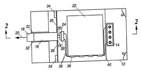
2 5 Referring now to FIG. 3, an illustration of a top plan view of a battery
pack 10 in accordance with the invention, and with the cover removed. A
pair of guide rails 32 guide the latch member 16 so that it can only travel in
the direction of arrow 20. Further, it can be seen in the drawing that the
spring means 26 used to bias the latch member is a pair of cantilevered arms
3 0 extending from the latch member. It is contemplated that the latch membercould be biased with only one cantilevered arm, or that a spiral wound spring
may be used instead of, or in addition to a cantilevered arm. The cantilevered
arms each bear against a corresponding support wall 34. Alternatively a
cantilevered beam could be disposed between the two supporting walls 34,
3 5 behind the actuating portion of the latch member.
SUBSTITUTE SHEET (RULE 26)
CA 02231~73 1998-03-10
WO 97/12414 PCTAUS96/15144
Further included in the battery pack 10 is an electronic switch circuit 36,
which is controlled by the mechanical switch 24. The electronic switch circuit
connects the battery cell 22 to the battery contact 14 when the latch member is
in the first position, as a result of the state of the mechanical switch, and
5 disconnects the battery cell from the battery contact when the latch member is moved to the second position. The mechanical switch is connected to the
electronic switch circuit by, for example, wires 38. The electronic switch circuit
is mounted on a circuit substrate 41D, preferably a flexible circuit substrate.
Referring now to FIG. 4, an illustration of a circuit diagram 50 for a
l 0 swikh circuit in accordance with the invention. There is shown therein at
least one battery cell 22, a mechanical switch 24, and an electronic switch
circuit 36. The latch member controls the operation of the mechanical switch,
and the mechanical switch controls the operation of the electronic switch
circuit. The electronic switch circuit comprises a semiconductor switch 52,
1 5 such as, for example, a MOSFET, having power terminals 54 and a control
terminal 56. The power terminals are connected in series between the
negative terminal 58 of the battery cell or cells and the battery contact 14. If a
MOSFET switch is used, it must be connected as shown due to the intrinsic
diode of the MOSFET. If it were reversed it would not block current in the
2 0 discharge direction, along arrow 60. A pull up resistor 62 is connected
between the control terminal 56 and the positive terminal 64 of the battery cellor cells. The mechanical switch 24 is connected in series with a pull down
resistor 66 between the control terminal 56 and the negative terminal 58 of the
battery cell or cells. The pull down resistor must have a significantly lower
2 5 value than the pull up resistor 62.
The disconnect switch circuit, comprised of the mechanical switch and
the electronic switch circuit, act to block current flow from the battery pack,
unless the latch member is moved to the second position, presumably as a
result of the battery pack being attached to the device. While the latch
3 0 member is in the first position, the mechanical switch is closed. From FIG. 4 it
can be seen that this results in the mechanical switch connecting the pull
down resistor 66 directly across the control terminal 56 and the negative
terminal 58 of the battery cell or cells. Since the pull down resistor is much
lower in resistance than the pull up resistor 62, the voltage at the control
3 5 terminal 56 with respect to the negative terminal 58 is very small, such that
the semiconductor switch 52 is off, and the battery cell or cells are
SUBSTITUTE SHEET (RULE 26)
CA 02231~73 1998-03-10
W O 97/12414 PCTrUS96/15144
disconnected from the battery contact 14. However, once the latch member is
moved to the second position, the mechanical switch 24 opens, thereby
disconnecting the pull down resistor from the control terminal 56. The pull
up resistor 62 provides the control terminal with a higher voltage, and the
S semiconductor switch closes, thereby connecting the battery cell or cells to the
battery contact 14.
In the case where the battery pack is not attached to the device, but the
disconnect switch circuit needs to be closed, such as when charging the battery
pack by itself, there is a need for a way to close the switch. In one ~lef~lled
l 0 embodiment the battery pack is provided with at least three contacts,
including battery contact 14, which as can be seen in FIG. 4, is the negative
contact of the battery pack. Typically there are provided one or two auxiliary
contacts in addition to the positive 67 contact and negative contact 14. A firstauxiliary contact, such as control contact 68, may be used for a first auxiliaryl 5 battery component 70, such as, for example, a thermistor, or a memory device.
Once the battery pack is inserted into a charger, an electric signal is applied to
the control contact to deLel~ e, for example, battery pack temperature. To
enable charging, a control network 72 is provided, and is connected between
the control contact and the control terminal of the semiconductor switch. Th~-
2 0 control network conditions the electrical signal and applies it to the control
terminal, causing the semiconductor switch to close, regardless of the latch
member. The control network does this by providing enough current to the
pull down resistor to produce a voltage across the semiconductor switch
sufficient to cause it to close. The actual design of the control network
2 S depends on the specific parameters of the system, such as what type of
electrical signal is applied to the control contact, and is left as a design choice
to the designer of the circuit. In many cases, however, the electrical signal will
be substantially a DC voltage, and the control network may simply be a diode-
resistor network.
3 0 While the preferred embodiments of the invention have been
illustrated and described, it will be clear that the invention is not so limited.
Numerous modifications, changes, variations, substitutions and equivalents
will occur to those skilled in the art without departing from the spirit and
scope of the present invention as defined by the appended claims.
SUBSTITUTE SHEET (RULE 26)