Note: Descriptions are shown in the official language in which they were submitted.
CA 02231825 2001-04-30
PRINTED CIRCUIT TRANSFORMER HYBRIDS FOR RF MIXERS
BACKGROUND OF THE INVENTION AND PRIOR ART
This invention related to transformer hybrids and
partial transformer hybrids used in RF mixers and
especially to such devices in broadband RF mixers (used in
television and satellite receivers) that operate up into
the gigahertz range of frequencies. As is well known,
operations at such frequencies make component
configurations, circuit layout, lead lengths and placement
extremely critical. This is one of the reasons
conventional ferrite core type coils and transformer
hybrids are difficult to use in high frequency broadband RF
mixer circuits. Another reason is the loss associated with
the ferrite material. The present invention utilizes a
construction technique that produces precisely controlled
transformer hybrid and partial transformer hybrid
configurations, minimizes lead length problems, reduces
losses and avoids much costly and time consuming labor.
OBJECTS OF THE INL'ENTION
The present _~nvention provides novel printed circuit
transformer hybrid and partial transformer hybrid
constructions.
The invention also provides printed circuit high
frequency transformer hybrid and partial transformer hybrid
constructions.
The invention also provides an improved broadband RF
mixer for operations up into gigahertz frequencies.
The present invention provides a high frequency hybrid
comprising:
a first substantially circular metallic foil element
divided into a f~z~st and a second portion;
a tab on one end of each of said first and second
portions;
1
CA 02231825 2001-04-30
a pad on each of the other ends of said first and
second portions;
a second substantially circular split metallic foil
element juxtaposed to said first element and including pads
on the open ends of said split element and a centrally
located tab;
an insulating substrate interposed between and
supporting said first and said second elements;
plated-througrh holes in said substrate and s<~id pads
electrically intez-connecting said pads of said first and
second elements;
a printed circuit board;
a rectangular aperture in said printed circuit board
for orthogonally ~~upporting said tabs and said substrate;
and
conductors on said printed circuit board for_ making
electrical conner:tion with said tabs.
In a further aspect, the present invention provides in
a wideband RF m:ixer of the type including symmetric
inductive means having first second and third windings,
means for coupling a symmetrical wideband RF signal to said
first and second windings and means for deriving an IF
signal from said third winding the improvement comprising:
said first arid second windings comprising a first
annular conductive element divided into first and second
portions and a second annular split conductive element
juxtaposed to said first element and separated therefrom by
an insulating substrate, with said first and second
portions being electrically interconnected with said second
element;
a third annular continuous conductive element for said
third winding; and.
an additional insulating substrate interposed between
said second element. and said third element.
The present invention also provides a wideband mixer
comprises:
a hybrid transformer having first, second and third
circuit windings;
la
CA 02231825 2001-04-30
said first and second windings comprising split
annular conductive elements separated by a first substrate;
said third winding comprising a continuous annular
element separated by a second substrate;
a partial hybrid transformer including fourth and
fifth printed circuit windings comprising split annular
conductive elements separated by a third substrate; and
means for coupling a symmetrical wideband RF s.ignal to
said first and second and said fourth and fifth windings
for deriving an I:F signal from said third winding.
l.b
CA 02231825 1998-06-10
BRIEF DESCRIPTION OF THE DRAWINGS
These and other objects and advantages of the invention will be apparent
upon reading the following description in conjunction with the drawings, in
which:
s FIG. 1 is a simplified schematic diagram of an RF mixer constructed in
accordance with the invention;
FIG. 2 is an exploded view of a printed circuit partial transformer hybrid
constructed in accordance with the invention;
FIG. 3 is an exploded view of a printed circuit transformer hybrid constructed
1 o in accordance with the invention;
FIG. 4 is a front view of the printed circuit transformer hybrid of FIG. 3;
FIG. 5 is a cross section taken along the line 5-5 of the transformer hybrid
of FIG. 4; and
FIG. 6 is a cross section taken along the line 6-6 of the transformer hybrid
Zs of FIG. 5.
DESCRIPTION OF THE PREFERRED EMBODIMENT
The term "transformer hybrid" appears for the device in FIG. 7.2 of
20 "MICROWAVE MIXERS" by Stephan A. Mass, copyright 1986. The term "partial
transformer hybrid" is used herein to describe a transformer hybrid without
the third
transformer winding.
Referring to FIG. 1, an RF mixer circuit 10 includes a symmetric amplifier
12 that drives the end terminals A, B of a partial transformer hybrid 14
consisting
2s of a two layer printed coil that is divided into two halves 13 and 15. A
center
2
CA 02231825 1998-06-10
terminal tab C connects the junction of coil halves 13 and 15 to ground
through a
capacitor 16. A source of DC voltage +V is connected to terminal tab C. A
transformer hybrid 26 with end terminal tabs D and E has a two layer printed
coil
that is divided into two halves 25 and 27 by a center terminal tab F. The
s transformer hybrid 26 may have the same type of coil construction as partial
transformer hybrid 14, but includes an additional third layer with a printed
coil
having end terminal tabs G and H. It will be appreciated that transformer
hybrid 26
incorporates a construction like that of partial transformer hybrid 14 with
the
addition of an added printed circuit IF pickup coil. The RF signal is supplied
to the
to center terminal tab F of transformer hybrid 26 and the IF signal is taken
from
terminal tab G and grounded terminal tab H. As is well known, the symmetrical
local oscillator (LO) signal from amplifier 12 causes ON/OFF commutation of
the
pairs of diodes 18,22 and 20,24.
The LO signal is not shunted by the " odd mode high impedance of the
15 partial transformer hybrid 14. The "even" mode RF signal is then coupled at
terminals D, E to the diodes 18, 20, 22 and 24 on the upper side of the diode
bridge and coupled to the AC ground by means of the partial transformer hybrid
14
on the lower side. Both partial transformer hybrid 14 and transformer hybrid
26
behave as short transmission lines (about 50-75 ohms characteristic impedance)
2 o for the RF signal propagating through partial transformer hybrid 14 and
transformer
hybrid 26 (even mode propagation).
In accordance with the invention, partial transformer hybrid 14 and
transformer hybrid 26 of mixer 10 are of printed circuit construction. In FIG.
2,
partial transformer hybrid 14 comprises coil halves 13a and 13b, and coil
halves
2 s 15a and 15b, that are juxtaposed on opposite sides of an insulated
substrate 30.
3
CA 02231825 2001-04-30
In practice, the coil elements are conductive foils on both sides of a thin
printed
circuit board (substrate 30) and are interconnected via two "plated-through"
holes
36, 46 and 38, 48 in respective ones of the two nested pads in the opposed
ends
of the coil elements. Even mode current flow proceeds via terminal A, through
coil
s element 13a, plated-through hole 36, 46, coil element 13b to terminal tab C.
Current flow in the other coil half proceeds via terminal tab B, through coil
element
15a, plated-through hole 38, 48, coil element 15b to terminal tab C. The
current
flow is thus seen to be in opposite directions in the overlaying coil elements
and
the transformer hybrid behaves therefore as a short (50-75 ohms) transmission
line
to for the even mode signal propagation.
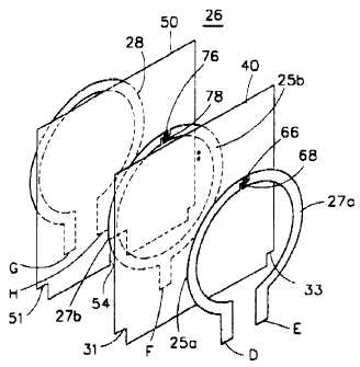
In FIG. 3, transformE:r hybrid 26 is indicated as including a 30 substrate 40,
with printed coil elements 25a, 25b, 27a and 27b, positioned in an arrangement
similar to that for partial transformer hybrid 14 in FIG. 2, and a substrate
50
supporting printed IF pickup coil 28. Insulated substrate 50 supports IF coil
28 in
15 juxtaposed, aligned position with respect to coil 35 elements 25a, 27a and
25b,
27b. The insulated substrates 40 and 50 preferably comprise thin glass or
Teflon
filled printed circuit boards upon which the conductive foil elements are
formed by
conventional printed circuit techniques. In the finished transformer hybrid
26, coil
elements 25a and 27a and 25b and 27b are formed on opposite sides of substrate
20 40 in juxtaposition to each other, and coil elements 28 is formed on the
far side of
substrate 50, which is cemented to substrate 40 to complete a "sandwich".
It will be noted that substrate 50 includes a small plated area 54 having a
plated
through hole 66 that is in alignment with terminal tab F that has a plated-
through
hole 64. Thus plated area 54 is electrically connected to terminal tab F by
means
25 of plated-through holes 64, 66.
4
Trade-mark*
CA 02231825 1998-06-10
Referring to FIGS. 4, 5 and 6, substrates 40 and 50 are seen to be
approximately
square shaped and include small corner cutouts 31, 53 and 51, 53. These
cutouts
cooperate with a rectangular aperture 60 in a printed circuit board 56 to
support the
substrates and conductive elements in an orthogonal position so that
conductive
strips 58 on printed circuit board 56 may be electrically connected to the
terminal
tabs.
The conductive strips 58 and terminal tabs are electrically connected as
indicated
by the solder fillets 68 and 70 in FIG. 5. Those skilled in the art will
readily
appreciate that, in certain situations, it may be desirable to position
conductive
1 o strips 58 on the other side of printed circuit board 56 and have the
substrates 40
and 50 extend through the printed circuit board. Soldering to the various
terminal
tabs would then be accomplished on the lower side of the-printed circuit board
shown.
It will be appreciated that the thickness dimensions of the substrate and foil
elements have been greatly exaggerated in FIGS. 4-6 to illustrate the
construction
details. In practice, the substrates are approximately 0.01 inches thick and
the foil
elements of even less thickness. The actual sizes of the elements if, of
course,
dependent upon design criteria for the devices and the frequency range
involved.
Manufacturing and installation techniques for components of these dimensions
are
2 o well known. Suffice it to say that the labor and uncertainty of
performance
associated with prior art baluns and transformers operating at frequencies in
the
gigahertz range are substantially eliminated with the invention.
What has been described is a novel printed circuit construction for high
frequency partial transformer hybrids and transformer hybrids and for RF
mixers
2 s utilizing such hybrids. It is recognized that numerous changes in the
described
5
CA 02231825 1998-06-10
embodiment of the invention will occur to those skilled in the art without
departing
from its true spirit and scope. The invention is to be limited only as defined
in the
claims.
6