Note: Descriptions are shown in the official language in which they were submitted.
CA 02231962 1998-03-11
TITLE~ OF THE INVENTION
DE~VICE AND METHOD FOR IDENTIFYING BANK NOTE
BACKGROUND OF THE INVENTION
Fielcl of the Invention.
The present invention relates to a device and
method for identifying a security or bank
note(hereinafter bank note) which can easily separate a
genui.ne bank note from. a false one.
Description of the Related Art
Recently use of various types of vending machines
has rapidly proliferated handling all sorts of
merchandise. Certain types of vending machines have
been introduced which can handle not only coins but also
bank notes. Since vending machines are set up in
various locations and undergo diversified operational
conditions, they are required to be able to perform
satisfactorily under all sorts of operational
:20 environments. This al:,o applies to mechanisms for
distinguishing genuine coins and/or bank notes from
false ones.
A mechanism for identifying genuine coins can be
constructed by a mechanical system, as false coins can
CA 02231962 1998-03-11
be separated from genuine ones by checking their weights
and/or shapes.
On the other hand, it has almost been impossible to
recognize genuine and false of a bank note by a
mechanical system, so that it has been conducted by
optically checking the extent of light transmission
through a bank note. In a conventional way of bank note
ident:ification a light source and a light receiving
element are positioned with specified distance between
them to transport a bank note therebetween for detecting
a bright-dark pattern peculiar with regard to the light
source to compare with a reference bright-dark pattern
stored in advance for determination of genuine or false.
However, in such a case, there existed a likelihood
of easily mistaking a copy of a bank note as a genuine
one, since identification of genuine or false has been
done only by means of a bright-dark pattern.
Use of a color sensor may be proposed to improve
this point but it is impossible to use such an expensive
device as a color sensor which recluires a complicated
signal processing for a vending machine for which low
production cost is an essential factor.
Further, it is re~uired to use an incandescent
light source (incandescent bulb) but an incandescent
CA 02231962 1998-03-11
light: source tends to be short lived and especially when
a vending machine is set up on a roadside under hot
summer sun, it is exposed to strong light and heat which
causes a breakdown of a bulb in a short while. In such
a case even a genuine bank note is mistaken as false
when it is inserted into such a vending machine making
it useless.
To solve those disadvantages, it may be proposed to
determine color tint of a bank note by employing, for
example, 2 light emitting diodes(LED), which emit lights
in different wavelengths as light sources and a light
receiving element which receives light emitted from each
of the LEDs. However, as LEDs have diversified light
emission characteristics, it was necessary to adjust
set-up positions and drive currents of LEDs to obtain
uniform performance ratio between 2 LEDs.
Further, in case of a vending machine which is
supposed to be set up in the out-doors, it is difficult
to maintain constant ratio of intensity of light emitted
:~0 by LE'Ds. This totally applies to a light receiving
element. This resulted in unreliable performance of a
bank note identification device and it was not suitable
for actual usage. To solve such disadvantages disclosed
in Japanese Examined Patent Publication No. 58-9478 is a
CA 02231962 1998-03-11
device which is provided with 2 LEDs, one of them being
green, while the other red, lights emitted from the 2
LEDs being received by a light receiving element and
cluant:ity of lights emitted by the 2 LEDs being
controlled so as to be ecfual, when there is no bank note
between LEDs and a light receiving element. When a bank
note comes between the LEDs and the light receiving
element, an error signal is to be generated, either if
an output of the light receiving element derived from
the light of green LED takes higher value than a
reference level indicating the color of the bank note is
incli.ned toward green in certain degrees or if the
output of the light receivi.ng element derived from the
light of the red LED takes higher value than the
reference level, indicating the color of the bank note
is ir,clined toward red in certain degrees.
However, the devi,-e in Japanese Examined Patent
Publication No. 58-9478 is based on a premise that when
the color of a bank note is not inclined (not shifted)
:20 toward red or green, the c~antity of light received by
the l.ight receiving element. put its output at zero level,
which is totally eclual to the output level found when
there is no bank note. It can only generate an error
signa.l in identifying such a bank note, when the color
CA 02231962 1998-03-11
of a bank note is shifted toward green or red in certain
degrees and it can be expected to have some effect only
for a bank note printed in certain colors but it was
almost impossible to identify bank notes printed in many
colors such as Japanese paper money.
For example, it can not generate an error signal
when a bank note is printed or copied in monochrome,
making it useless under actual circumstances.
SU ~ARY OF THE INVENTION
It is an object of the present invention to provide
a device and method for solving the aforementioned
probl.ems. It is another object of the present invention
to provide a device and method for identifying a bank
note which is highly reliable and easily manufactured
.15 and a.djustable and capable to automatically solve
problems such as variation of performance of each
components of the detection mechanism of the
identification device, change due to aging and change in
performance due to surrounding environment with simple
:20 construction.
To attain such objects the present invention
provide a device and method for identifying a bank note
comprising first light emitting means for emitting light
in a specified wavelength, second light emitting means
CA 02231962 1998-03-11
emitting light in a wavelength different from that of
the iirst light emitti.ng means, first drive means for
driving the first light emitting means to emit light,
second drive means for driving the second light emitting
means to emit light, l.ight emission control means for
activating the first a,nd second drive means by
sec~uentially switching them, light receiving means for
outputting electrical signals corresponding with
detected light intensity by receiving both of lights
emitt:ed from the first and second light emitting means,
adjustment means for a.djust:ing intensity of light
emission by adjusting at least one of the first and
second drive means so as to keep the difference in the
level. between electric signals generated in the light
lS recei.ving means corresponding with the lights with
different wavelengths from each of the light emitting
means within a specified range to eliminate variations
in performance of the each light emitting means and the
light. receiving means, means for fixing light intensity
:20 to fix adjusted state of the adjusting means when an
object to be identified reaches between both of the
light. emitting means and the light receiving means,
extra.cting means for extracting alternating current
compcnent of the electrical output signals from the
CA 02231962 1998-03-11
light: receiving means during transportation of the
object to be identified between the light emitting means
and t:he light receivin.g means, and sampling means for
sampling alternating current output signal value in the
alternating current ou.tput signal from the extracting
means at the time of receiving light from either one of
the light emitting means, whereby identification of a
bank note is conducted based on the sampling value from
the sampling means.
Further, for example, the invention is
characterized to conduct identification of a bank note
by checking the extent of similarity between a sampling
value derived in the sampli.ng means and the value of a
genui.ne object to be identi.fied stored in advance. Or
else, in another embodiment., the invention is
characterized by constructing the first and second light
emitt.ing means with LEDs, arranging both of the LEDs and
the l.ight receiving means opposedly facing each other,
the object to be identified being transported between
:20 the first and second LEDs and the light receiving means,
while an optical filter may be disposed between the
first. and second LEDs and the light receiving means.
In another example, the invention is characterized
by cc,nstructing the first and second light emitting
CA 02231962 1998-03-11
means with LEDs, disposing the light receiving means
between the first and the second LEDs so as to be able
to receive lights emitted from both of the LEDs after
they are reflected from a reference reflector, while an
object to be identified is transported between the first
LED, second LED, the light receiving means and the
refer-ence reflector.
These and other o:bjects and features of the present
invention will be apparent by referring to the following
:10 detailed description of the embodiments of the invention,
taken. together with the accompanying drawings.
BRIEF DESCRIPTION OF THE DRAWINGS
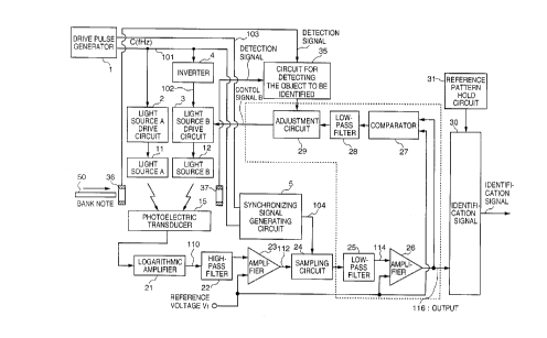
FIG.l is a block diagram illustrating construction
of a device for identifying bank note according to an
:15 embod.iment of the present invention.
FIG.2 is a block diagram illustrating detailed
construction of the circuit for automatically adjusting
inten.sity of light emission from light sources shown in
FIG.l
FIGS.3A and 3B are drawings illustrating
arran.gement of the light emitting elements and the light
receiving element in an embodiment of the present
inven.tion.
FIG.4 is a time chart for explaining the operation
CA 02231962 1998-03-11
of the embodiment shown in FIG.l of the present
invention.
FIG.5 is a drawing illustrating a color chart
sample and relative direction of movement of
ident:ification position.
FIG.6 is a graphic presentation illustrating an
example of result of reading-out of a color chart sample
according to an embodiment of the present invention.
FIG.7 is a graphic presentation illustrating the
result of reading-out of a monochrome copy of the color
chart sample according to an embodiment of the present
invention.
FIGS.8A and 8B are drawings illustrating
arrangement of the light emitting elements and the light
receiving element in the second embodiment of the
present invention.
FIG.9 is a block diagram illustrating detailed
construction of the circuit surrounded by broken lines
in FIG. 1 in another embodiment of the present invention.
DETAILED DESCRIPTION OF THE PREFERRED EMBODIMENTS
Now referring to the drawings, an embodiment of the
invention will be described in more details.
[First Embodiment]
FIG.l is a block diagram illustrating construction
CA 02231962 1998-03-11
of a device for identi.fying bank note according to an
emboc~iment of the present invention. FIG. 2 is a block
diagram illustrating dLetailed construction of the
circuit for automatically adjusting intensity of light
emission from light sources showr.L in FIG.l. FIGS. 3A and
3B are drawings illustrating arrangement of the light
emitt:ing elements and the light receiving element in an
embocliment of the present invention and FIG.4 is a time
chart for explaining the operation of the embodiment
shown in FIG.l of the present invention.
In FIG.l, a drive pulse generator 1 for generating
refer-ence drive pulses of this embodiment generates and
outputs a reference clock signal 103(frecluency 2f) along
with light source A drive pulse 101 (frec~uency f) which
is obtained by dividing the reference clock signal 103.
In this embodiment the pulse frec~uency f is set at 4 KHz.
A light source A drive circuit 2 controls emission
of li.ght from the light source A 11. A light source B
drive circuit 3 controls emission of light from the
light. source B 12. The light source B drive circuit 3
controls cluantity of light emission from the light
source B 12 in response to control signal B from an
adjustment circuit 29. An inverter circuit 4 generates
light. source B drive pulse 102 by reversing light source
- 10 -
CA 02231962 1998-03-11
A drive pulse 101.
A synchronizing signal generating circuit S
generates sampling pulses 104 from reversed signal of
the reference clock 103 and light source A drive pulse
101 cmd then feed the~l into a sampling circuit 24.
A light source A 11 iS, for example, a red LED
emitt:ing red light ancL a light source B 12 is a LED
emitt:ing light in a different wavelength from light
source A, for example, in green. AS shown in FIG. 4,
the ]ight source A 11 and light source B 12 are driven
to emit lights by oppositely phased drive pulses 101 and
102, respectively, ancl are controlled to emit lights in
an a]ternate sequence.
A photoelectric transducer 15 receives lights
emitt:ed from the light source All and the light source B
12 to convert them to output electric signals
corresponding to the quantity of received lights and may
consist of, for example, a photo diode. A logarithmic
amplifier 21 amplifies electric signal from the
photoelectric transducer 15.
In this en~odiment of the present invention, value
of received light signal (value of signal for detecting
ratio of light intensity of the light source 11 to that
of the light source 12)from the photoelectric transducer
CA 02231962 1998-03-11
15 is amplified by a logarithmic amplifier 21, because,
if a linear amplifier is used, it is basically
impossible to eliminate shifts related to such absolute
value components of light emission intensity as
deviations in distance between a light source and a
photoelectric transducer, intensity of emitted light and
sensitivity to received light or temperature
characteristics and deterioration, as absolute value
components of intensity of emitted lights essentially
come out in the output of the linear amplifier when an
object to be identified is inserted between the light
sources A 11 and B 12 and photoelectric transducer 15,
while if a logarithmic ampl.ifier is used, it is possible
to obtain output only related to property of an object
to be identified. Moreover, a method is adopted in
which difference of outputs of the same logarithmic
ampli.fier is taken, because it allows to eliminate need
for Is cancellation intrinsic to a logarithmic amplifier,
which enables to simplify design of the logarithmic
ampli.fier itself.
Namely, if a linear amplifier is used,
V ~ (Ma + N)-(Mb + N) = Ma - Mb
where, V is the wave height value, Ma the light
intensity of the source A 11, Mb that of the source B 12,
CA 02231962 1998-03-11
common steady-state ba.ckground N.
If a logarithmic amplifier is used,
V ~ ln(Ma + N) - ln(Mb + N) =ln{(Ma + N)/(Ma + Mb)}
When automatic adjustment is implemented so as to
make the value of the wave height to be 0,
if a linear amplifier is used,
Ma - Mb = O .. Ma = Mb
while, a logarithmic amplifier is used,
(Ma + N)/(Mb + N) = 1 .. Ma = Mb
Consecluently, both cases result in the same light
emission condition.
However, under the above condition Ma = Mb (-C),
if an object to be identified with light
transmittances(or reflectances) a and b for the lights
from the sources 11 and 12, respectively, is inserted
between the sources A 11 and B 12 and photoelectric
transducer 15, the wave height value V is, for a linear
amplifier,
V ~ aMa - bMb =(a. - b)C
which. shows that an absolute value component C in
inten.sity of light emission appears in the output,
while for a logarithmic amplifier,
CA 02231962 1998-03-11
V ~ ln{(aC + N)/(bC + N)}
which can be expressed approximately as,
V ~ ln{(aC )/(bC)} = ln(a/b)
under a condition aC, bC >> N (N may be non-steady
state), which enables to obtain only property of the
object to be identified, even though with some
conditions. This is a reason why a logarithmic
ampli.fier is used in the individual embodiment of the
present invention.
A high-pass filte:r 22 eliminates components less
than f (direct current component and fluctuation related
to brightness produced between direct current and f ) in
the cLetected electric signal from the logarithmic
amplifier 21 to extract alternating current components
synch.ronized with the drive pulses 101 and 102.
An amplifier 23 superposes the reference direct
current Vl over output of the high-pass filter 22 for
output. A sampling circuit 24 samples the output
signa.ls from the amplifier 23 by means of sampling pulse
104 from synchronized signal generating circuit 5 to
hold and output the sampled value.
In this embodimen-t of the present invention, the
sampling pulse from the synchronized signal generating
circuit 5 is outputted in synchronization with the
- 14 -
CA 02231962 1998-03-11
timing of emitted light reception from the source A 11
to obtain output corresponding to difference of cluantity
of received light from both of the sources A 11 and B 12.
A low-pass filter 25 eliminates frecluency (f)
component and its harmonic components in the drive
pulses 102 and 103 from output signal of the sampling
circuit 24. An amplifier 26 amplifies the output from
the low-pass filter 25 in a specified ratio with
reference to the reference voltage V1 to output signal
amplified by amplifica.tion factor k of the amplifier 26.
By the way, at the time of the automatic adjustment of
cluant:ity of light from the light source (at the time of
negat:ive feed-back) its output becomes as V1.
In this embodiment of the present invention, a
circuit for automatic adjustment of intensity of light
emission from the ligh.t source which is shown in the
following description is added to eliminate need for
adjustment of position.ing of LEDs and adjustment of LED
drive current for getting uniform performance ratio to
cope with variation in light emission characteristics of
LEDs and to maintain ratio of intensity of light
emission from the source A 11 to that from the source B
12 acrainst large fluctuation in conditions of
surrounding environment with simple construction without
CA 02231962 1998-03-11
fail, even when the device of the present invention is
used in a vending machine which may be set-up in the
outdoors .
In this circuit a. comparator 27, a low-pass filter
28 and an adjustment circuit 29 are arranged to conduct
adjustment of intensit:y of light emission from the
source B 12 to attain adjustment of ratio of intensity
of light emission from the source A 11 to that from B 12.
The comparator 27 compares voltage of output signal
of the amplifier 26 wi.th the reference voltage V1 to
automatically adjust l.ight emission of the source B 12
so as to ec~ualize output signal of photoelectric
transducer 15 corresponding with cluantity of the
received light from the source A 11 with that from B 12,
when there is no object to be identified, for example, a
bank note between the sources A11, B 12 and the
photoelectric transducer 15. The comparator 27
generates OV, if, for example, the output voltage of the
ampli.fier 26 is higher than the reference voltage V1,
and qenerates a specified voltage as it comes to a
saturated state, if the output voltage of the amplifier
26 is lower than V1.
The low-pass filter 28 eliminates alternating
current component in t.he output of the comparator 27 and
CA 02231962 1998-03-11
feeds the resulting si.gnal to the adjustment circuit 29.
Name]y, the output vol.tage of the low-pass filter 28
shift:s to lower level than the present level, if the
output from the comparator 27 is 0V, while it moves
toward higher level th.an the present level, if the
output from the comparator 27 is in the saturated state.
It comes to be stabilized finally at a certain voltage
leve].
When a circuit 35 for detecting an object to be
ident:ified indicates that no object is detected, if the
output signal of the low-pass filter 28 shifts to lower
voltage, it indicates that the intensity of light
emission from the source A 11 is found to be higher than
that from B 12 in comparison of light from A 11 with
that from B 12 looking from the photoelectric transducer
15 and then the adjustment circuit 29 controls the
contr-ol signal B so as to enhance light emission of the
source B 12 by increasing the drive current from the
source B drive circuit 3.
On the other hand, if the output signal of the low-
pass filter 28 shifts to higher voltage, it indicates
that the intensity of light emission from the source B
12 is found to be higher than that from A 11 in
comparison of light emission from A 11 with that from B
CA 02231962 1998-03-11
12, ]ooking from the photoelectric transducer 15 and
then the adjustment circuit 29 controls the control
signal B so as to reduce light emission of the source B
12 b~r decreasing the d.rive current from the source B
drive circuit 3. The aforementioned control process is
repeated until the output voltage of the amplifier 26 is
ecfual.ized with the reference voltage V1. By controlling
as described above, it is possible to conduct automatic
control so as to ecfualize the detected signal output of
photoelectric transducer 15 corresponding with light
emission from the source A 11 with that from the source
B 12. As a result, an~y error in positioning the sources
A 11 and B 12 or any variation in standards and
speci.fication of the light sources can be automatically
elimi.nated. Further, any influence caused by
deterioration of the light source due to aging or any
variation in the performance of the light source or the
photoelectric transducer 15 due to environmental change
can be automatically eliminated.
This makes it not necessary to conduct cumbersome
adjustment works as recfuired in the past to enable to
cope with the fluctuation of set-up environment without
any zdjustment.
The adjustment ci:rcuit 29 conducts above control
- 18 -
CA 02231962 1998-03-11
and works to maintain the state of the control signal B
at the time just before output of signal indicating
detection of an object to be identified and stops
adjustment based on the output signal from the low-pass
filter 28, when such signal is generated from the
circuit 35 for detecting the object to be identified.
When generation of the signal indicating detection of an
object to be identified is stopped from the circuit 35
for cletecting the object to be identified, the
adjustment circuit 29 resumes above control process to
control the control signal B so as to stabilize voltage
of the output signal of the low-pass filter 28 at a
certain voltage.
It is not necessarily recfuired to keep doing above
mentioned adjustment at all times, when there is no
object to be identified and control may be started by
activating the light sources with signals set before
generation of the signal indicating detection of an
object to be identified. Or else, the control signal B
may be maintained within an acceptable range by
activating the light sources once in every specified
time interval to conduct control so as to extend life of
the light sources by preventing exhaustion of the light
source during time of waiting the object to be
- 19 -
CA 02231962 1998-03-11
identified.
The circuit 35 fc,r detecting the object to be
ident:ified generates t:he signal indicating detection of
an object to be identified to feed it to the adjustment
circuit 29 indicating that an object 50 to be identified
such as a bank note is transported to the location in
the transportation pat:h where the sources 11 or 12 and
photoelectric transducer 15 is positioned, while either
a sensors 36 or 37 for detecting an object to be
ident:ified is detecting transportation of an object to
be iclentified.
The sensor 36 for detecting an object to be
ident:ified is, for example, disposed at a upstream
posit:ion adjacent to the sources 11 and 12 in the
transportation path of an object to be identified and
the sensor 37 for detecting an object to be identified
is di.sposed at a downstream position adjacent to the
sources 11 and 12 in the transportation path of an
object to be identified.
Shown in FIG. 2 is an example of circuit
const:ruction of the ak,ove described circuit for
automatic adjustment of intensity of light emission of
the light source.
In FIG. 2, a comparator 27a consisting of the
- 20 -
CA 02231962 1998-03-11
comparator circuit 27 generates 0V when voltage of the
OUtp~lt 116 from the amplifier 26 is higher than the
reference voltage Vl, while it comes to saturation, when
it is lower than Vl.
In the circuit of FIG. 2, control of control
suspension of the cont:rol signal B at the time of output
of the signal indicati.ng detection of an object to be
ident:ified from the ci.rcuit 35 for detecting an object
to be identified is conducted by an analog switching
circuit which is integrated with low-pass filter part.
The voltage of output signal of the low-pass filter part
at the time when no ou.tput of the signal indicating
detection of an object to be identified is generated
from the circuit 35 for detecting an object to be
identified shifts to lower level than the present level,
if the output of the comparator 27a is 0V and to higher
level., if it is in a saturated state. It comes to final
stabi.lization at a certain voltage.
A sample and hold part works simply as a buffer
when no object to be identified is found and the low-
pass filter output as it is is generated as the control
signal B. As a result, if it shifts to lower voltage,
the source B 12 drive current is increased as the source
A 11 intensity is higher and if it shifts to higher
- 21 -
CA 0223l962 l998-03-ll
voltage, the source B 12 drive current is decreased as
the source B12 intensity is higher.
FIGS. 3A and 3B show an example of arrangement of
the source A 11, B12, the photoelectric transducer 15
and t:he sensors 36 and. 37 for detecting an object to be
ident:ified shown in FIG. 1.
In FIG. 3A an object to be identified is transported
in a direction perpend.icular to the surface of the
drawi.ng and in FIG. 3B it is transported from the left-
hand side of the drawing to the right-hand side. As
shown in FIGS. 3A and 3B, the sources A 11 and B 12 are
disposed with a specified distance between them, both of
their light emission surfaces being directed toward the
photoelectric transducer 15 so as to make the maximum
cfuant.ity of their light emission reach to the
photoelectric transducer 15.
Sensors 36 and 37 are disposed in the upstream side
and clownstream side, respectively, along the
transportation path of the object 50 to be identified
adjacent to the range of reach of the lights emitted
from the sources A 11 and B12 to the photoelectric
transducer 15, so as to enable to detect arrival of the
object to be identified at the detection range, when it
is ca.rried to the detection range either from the
CA 02231962 1998-03-11
upstr.eam side or the d.ownstream side.
In FIG. 2 a color filter 40a is disposed between
the sources A 11, B 12 and the photoelectric transducer
15, i.f required, for adjusting wavelength of light which
can be detected with better sensitivity corresponding
with color of an object to be identified. This enables
to acljust sensitivity to a certain color, if color of a
bank note to be identified is inclined toward a certain
color-. The color filter may be disposed either between
the light sources and the object to be identified or
between the object to be identified or the photoelectric
transducer 15.
In this embodiment of the present invention, the
direction shown in FIG.3B is selected as one with least
off-set of light impinging on the object to be
identified from the sources 11 and 12. This arrangement,
of ccurse, may be made as optional.
Now, the way of control for identification of the
object to be identified in this embodiment of the
present invention wit the above construction is
described. In this e~odiment of the present invention,
the detection output 116 is controlled so as to make it
equal as the reference voltage Vl and the logarithmic
ampli~ier output is controlled at a certain voltage
- 23 -
CA 02231962 1998-03-11
level, before the object to be identified reaches within
the cletection range.
When the object to be identified arrives at the
detection range under such a controlled state as the
cluantity of light emission from the sources A 11 and B
12 is fixed, the photoelectric transducer 15 generates
electric signal corresponding with wavelength of emitted
light from the sources 11 and 12 or wavelength through
the color filter trans~mitted through the object to be
identified. It, then, is amplified in the logarithmic
amplifier 21 and is fed to the high-pass filter 22.
Suppose, for example, the light source A 11 is a
red L,ED, while B 12 a green LED. I n this case,
detected signal has higher output voltage value at a
timing of the source A emission than at a timing of the
source B emission, if the color of the object to be
identified in the detection range is more inclined to
red than green or intensity of transmitted light from
the source A 11 is higher than that from B 12. To the
contrary, detected signal has higher output voltage
value at a timing of the source B emission than that at
a timing of the source A emission, if the color of the
object to be identified in the detection range is more
inclined to green than red or intensity of transmitted
- 24 -
CA 02231962 1998-03-11
light from the source B 12 is higher than that from A 11.
The example shown in the left-hand side in the
timing chart of FIG. 4 indicates a case in which
detected signal has higher output voltage value at a
timing of the source A emission than at a timing of the
source B emission, wit:h the color of the object to be
idenlified in the detection range being more inclined to
red lhan green, while the right-hand side of FIG.4
indicates a case in which detected signal has higher
OUtpllt voltage value at a timing of the source B
emission than at a timing of the source A emission, with
the color of the object to be identified in the
detection range being more inclined to green than red.
The high-pass filter 22 eliminates less-than-f
components in the detected signal to extract alternating
current component higher than f. Then the signal is
superposed with the reference voltage Vl in the
amplifier 23 for sampl.ing, in the sampling circuit
24,the wave form data in the superposed wave form at the
timing of detection of light emission from the source A
11 to hold it until the next sampling timing.
In this embodiment of the present invention, since
the aLmplifier 23 generates output signal which
fluctuates either to t.he positive side of the reference
- 25 -
CA 02231962 1998-03-11
voltage Vl or to the negative side thereof in proportion
to the variation of c~Lantity of detected lights from the
sources A 11 and B 12 or the difference between the
detec~ted signals of the photoelectric transducer when it
rece ves the lights from both of the light sources, it
is possible to detect to what extent the color of the
object to be identified is inclined to red (when it
swings to the positive side) or to what extent it is
inclined to green (when it swings to the negative side)
by only sa~Lpling detected signal at the timing of
detecting light emission from the source A 11.
As a result there is no need to conduct color-by-
color identification for a plurality of colors in the
true--or-false identification process for a bank note
described later. This enables to simplify construction
in a large measure as it is possible to determine to
what color the object to be identified is inclined out
of a plurality of colors by simply checking only one
kind of detected signal.
Then, the signal level of the result of sampling in
the sampling circuit 24, which is the difference of the
detected signal or difference of the color tint at the
time of receipt of lights emitted from both of the
sources A 11 and B 12 by the photoelectric transducer 15,
- 26 -
CA 02231962 1998-03-11
is amplified to be fed. to a identification part 30. As
shown in FIG. 4 the color inclination of the object to
be iclentified against the lights emitted from both of
the source 11 and 12 is generated as one signal.
Accordingly, the identification part 30 following
to the amplifier 26 compares an output pattern in the
output signal 116 by slicing it in a specified time
frame with a reference pattern stored in the reference
pattern storing part 31 which is to be obtained when a
genui.ne bank note is detected to determine the degree of
similarity. The object to be identified is determined to
be genuine, if similarity is found to be in excess of a
specified degree.
As for such reference patterns, only one reference
pattern is suffice to be stored for comparison for each
bank note to be identified, enabling to make
identification process simpler. On top of that, it can
aptly cope with errors of almost all colors, as it can
handle errors of a plurality of colors, even though
comparison with only o:ne reference pattern is
implemented.
As a result, it is possible to distinguish properly
the genuine from the false, even when the object to be
identified has only one side of a bank note printed on
CA 02231962 1998-03-11
both sides or a double sided copy or single sided copy
made by a duplicator.
The above mentioned light sources A 11 and B 12 are
not necessarily limited to independent discrete LEDs but
they may be integratecl into a 2-colored LED. Such a
construction will serve to simplify design by reducing
mounting of a LED in only one location.
An example of detection using an actual color chart
with the construction shown in FIG. 1 is described in
FIGS. 5 to 7.
Following reading-out was conducted by means of a
const:ruction using a 2-colored LED integrating red and
green LEDs in one piece. In this example, a 2-colored
LED is disposed so as to arrange 2 LED chips, each red
and qreen, side by side to form a right angle to the
line of transportation with the red diode chip working
as the source B in the construction of FIG. 1.
A color chart sample of FIG. 5 is transported
between the sources 11, 12 and the photoelectric
transducer 15 at a speed of some 160 mm/sec. FIG. 5
shows the color chart only in ll]m;n~nce or in monochrome.
FIG. 6 illustrates graphically an example of the
output signal 116 of the amplifier 26 with the reference
voltage V1 being set at 5 v in the construction of FIG.1.
- 28 -
CA 02231962 1998-03-11
As illustrated in FIG. 6 colors with the hues of
red, orange, yellow and purple show swings toward lower
level.s than the reference voltage, while those with the
hues of green and blue toward higher levels. This shows
that there is a certain rate for each color in level of
output value. As a result, when bank notes of a same
kind in different condition are read out, the variations
in wave forms based on the reference voltage Vl for each
of bank notes in different condition falls within a
certa.in range, if we compare the wave forms for each
bank note in different condition based on the reference
voltage Vl, even though bank notes of same kind in
different conditions show different output signals in
the detection stage at the photoelectric transducer 15.
Accordingly, it is possible to attain high degree
of identification of genuine or false by comparing the
wave form of an actual read-out signal based on the
reference voltage Vl with a stored pattern, if a
repre~sentative pattern of detected wave form for certain
kind of bank note is stored in advance as a reference.
FIG. 7 illustrates an example of output 116
obtained by transporting, in a similar way, a monochrome
sample copy which was :made by monochromatically copying
of the color chart sample of FIG. 5 with a duplicator.
- 29 -
CA 02231962 1998-03-11
As shown in FIG. 7, the output 116 does not
indicate much fluctuat:ion, when there is only difference
in lightness with no variation of chroma. Needless to
compare with the wave form of FIG. 6, it takes quite a
different wave form which makes it very easy to separate
the i-alse from the genuine.
As described above, it is possible to provide a
device which is highly reliable and easy to manufacture
and adjust and capable to automatically solve problems
such as variations of performance of each components of
the mechanism for detecting object to be identified,
chanqe due to aging and change in performance due to
surrounding environment with simple construction.
It also enables to conduct reliable identification
of genuine or false with a simple algorithm, since it
can express color difference between a genuine one and
an object to be identified by one output signal in the
detection result of the object to be identified.
[Second Embodiment]
The above description is made for an example in
which the lights transmitted through an object to be
ident:ified from the light sources are detected by means
of a photoelectric transducer 15. The present invention
is, however, not limited in the above case but also may
- 30 -
CA 02231962 1998-03-11
be applied to a case in which the lights emitted from
the sources are reflected through an object to be
ident:ified so as to detect the reflected lights by means
of a photoelectric transducer 15. A second embodiment
of the present invention which is constructed as above
is described below referring to FIGS. 8A and 8B. The
second embodiment has a similar basic construction as
the f~irst embodiment shown in FIG. 1 described above but
arrangements of the sources A 11, B 12 and the
photoelectric transducer 15 is different. Those parts
of the second embodiment different from the first
embocLiment is described below.
FIGS. 8A and 8B illustrate arrangements of the
sources A 11, B 12, the photoelectric transducer 15,
sensors 36 and 37 for detecting an object to be
ident.ified in the second embodiment of the present
inven.tion. In FIG.8A an object to be identified is
transported in a direction perpendicular to the surface
of th.e drawing and in FIG. 8B it is transported from the
left-hand side of the drawing to the right-hand side.
As sh.own in FIGS. 8A and 8B, in the second embodiment of
the present invention, the sources A 11 and B 12 are
disposed so as to sandwich the photoelectric transducer
15. A reflector 45 for reflecting the lights emitted
CA 02231962 1998-03-11
from the sources A 11 and B 12 is disposed under the
transportation path of the object 50 to be identified.
The mounting positions of the sources A 11 and B 12
may be determined so as to make the reflected lights
from the reflector 45 to impinge on the photoelectric
transducer 15. Such construction allows to dispose the
light: sources and the photoelectric transducer in
adjacent locations to form an integrated optical system
and to make the whole system in a compact size. Also,
it is easy to make the reflector with a function of a
color filter which can reflect a certain color better or
less.
[other embodiment]
In the above descriptions, examples are shown in
which. red and green LEDs are used for the light sources.
Howev-er, the present invention is not limited to the
above examples but it can be applied to other
embodiments which use light emitting devices with
varicus wavelengths as long as 2 light sources have
different wavelengths. For example, a combination of a
red L,ED and a (green + infrared) LED or a combination of
a red LED and infrared LED may be employed and it is
suffice to use a combination of 2 kinds of LEDs and not
necessarily restricted by wavelengths. Also, it is not
CA 02231962 1998-03-11
recluired to form 2 light sources by employing separate
LEDs but they can be i.ntegrated in a two-colored LED as
the example of reading-out of a sample stated above.
The duty factor of the drive pulse of the light
source is set at 50% in the description but it is not
necessarily limited tc 50 % but also any duty factor may
be employed.
In the above description, described is a case in
which analog signal is used for the output signals to
the circuit for controlling light emission of the source
B 12 encircled by a broken line in FIG. 1 and to the
ident:ification circuit 30. However, the present
invention is not limited to the embodiment in which
signal is processed in analog but it may be applied to
cases in which signal is processed in digital by analog-
to-digital conversion. In such cases, the output signal
of th.e sampling circuit 24 is converted in an analog-to-
digit.al conversion circuit to digital signal
corresponding with the analog signal to send it to the
ident.ification circuit 30 in which the detected digital
signa.l is compared with the reference pattern stored as
digital signal in the reference pattern storing part 31
for digital pattern matching.
In this case, the comparator 27 in the circuit for
- 33 -
CA 02231962 1998-03-11
controlling light emicsion of the source B 12 compares
the cletected digital ciignal value with a digital
reference value corresponding with the reference signal
Vl to make the difference of 2 digital signals as up-
count: pulse or down-count pulse of an up-down counter.
The count value of the up-down counter may be used as
the control signal B by digital-to-analog conversion.
When the part 35 for detecting an object to be
identified generates signal to indicate detection of an
object to be identified, count value of the up-down
counter may be kept in a hold-state. FIG. 9 shows an
embodiment of such construction.
Various modifications and alterations of the
present invention may be constructed without departing
the spirit and scope of the invention. It should be
understood that the present invention is not limited to
the specific embodiments described in this specification.
To the contrary, the present invention is intended to
cover various modifications and ecluivalent arrangements
included within the spirit and scope of the claims.
- 34 -