Note: Descriptions are shown in the official language in which they were submitted.
CA 02232162 1998-03-16
W O 97/11332 PCTABR96/00041
Specification
DEVICE AND PROCESS FOR DETERMINING FILM
THICKNESS AND PATTERN REGISTER IN CELLS PLATED ON
INDUCTIVE DEBIT CARDS
s The present invention refers to the determination of thickness of
conductive metal layers deposited over ins~ ting surfaces, and more
specifically to the thickness measurement of the metal film employed in the
production of credit cells on inductive debit cards such as those described in
the patent documents PI(BR) 7804885, PI(BR) 9201380-5 and PI(BR)
0 9304503-4, here incorporated by reference.
Methods for measuring the thickness of metal layers based on
X-ray diffraction are already well known, however their cost, as well as the
time required by them restrict their use to high precision measurements in
laboratories.
Moreover, the currently known methods do not detect
adequately the register errors that crop up in the card's m~nllf~cture, i.e., the
position mi~m~tch of the metallic cell pattern plated over the card with
relation to its edges.
In view of the above, the present invention has as its major aim
20 the provision of a device capable of measuring expeditiously the thickness of said metallic films, with minim~l error margin and at low cost.
An additional objective is the detection of faulty register during
the plating of cells, i.e., the mi~m~t~h between the real position of those cells
and the ideal one in relation to the card edges, said mi~m~tch rendering the
25 card useless.
The above aims are accomplished by the invention by means of
a device compri~ing a sensing assembly consisting of a plurality of sensing
modules, each module consisting of an oscillator wherein the inductance is
provided by a sensing coil coincicl~nt~lly placed at true position of its relative
30 credit cell, each sensor being, one at a time, individually enabled by a pulse
origin~ted by Co~ illg means which control the process, the oscillator
output voltage being coupled to means for converting it into a numerical
value, to be processed by said coln~u~ g means according to coefficients
stored in memory means so as to inform the thickness of the metal layer.
According to another feature of the invention, said coefficients
are previously determined for each one of the positions in the cell array by
means of individual callibration, using standard cards of known metal film
CA 02232l62 l998-03-l6
PCT~BR96/00041
W O 97/11332
t'nickness.
According to a further feature of the invention, sensors placed
outside the cell matrix are provided. to enable the measurement of register
errors in the plated cell pattern.
s According to yet another feature of the invention, the device
allows the integrity check of all cells in the card, thus perrnitting the rejection
of those cards in which one or more cells are open due to manufacturing
defects.
The previous characteristics, as well as other aspects and
o advantages of the present invention, will become more evidente from the
description of a specific embo-liment, taken as an example and not in a
limiting sense, as shown by the attached drawings in which:
Figure 1 shows the block diagram of the test device built
according to the principles of the invention, as well as its connections to
extern~l control equipment, such as a PC-compatible micro-co~ uler.
Figure 2 shows a more detailed view of the proposed device,
according to the invention.
Figure 3 illustrates a calibration curve for one sensing module,
showing the elements which allow conversion of the measured voltage values
into metal layer thicknesses, according to the invention.
Figure 4 shows the principle of register mi~lignment detection,
according to the invention.
Referring now, more specifically, to the block diagram in figure
1, the proposed device 20 comprises the following blocks:
2s ~ Control board 21-- CPU-A/D -- consisting of micro-controller, analog to
digital converter (A/D), memories and accessories;
Decoding card CEO 22, consisting of the address decoders, which controls
the operation of each oscillator in the sensor matrix by means of
individual lines 23;
~ Sensing assembly 27, consisting of as many sensing modules as the
number of cells in the card, each of these modules con~ining, in addition
to the oscillator, a pair of colinear sensing coils 24a - 24b, the internal
ends of their cores forrning a gap into which lies a credit cell 25, the width
of said gap being slightly greater than the card thickness, to allow for
accidental irregularities.
Still according to figure 1, device 20 is connected to a PC
microcomputer 11, which controls the measuring process through a serial
CA 02232162 l99X-03-16
W O 97/11332 PCT~BR96/00041
comm-mication line 46 m~king use of a standardized protocol such as, for
instance, the RS 232.
Referring now to figure 2, it can be seen that the sensing
assembly 27 comprises a plurality of test modules 30, each one consisting of
s a Colpitts oscillator in which the coils that make up the tank are the inductive
sensors 24a and 24b. Such oscillators have the property of producing an
altern~ting signal whose amplitude is proportional to the inductive coil
loading. Considering that said loading depends on the characteristics
(thickness, conductivity) of the metal layer, as well as on the cell condition
o (open or shorted), it follows that for a known alloy, the signal amplitude
between the leads of the sensing coil will be inversely proportional to the
thickness of the metal film.
Transistor 31 in all oscillators is normally cut-off, the
oscillation being enabled individually by block CEO 22 through a positive
voltage pulse 32 applied to the transistor's base through one of the lines of
group 23. Duration 33 of this pulse is sub t~nti~lly greater than the time
needed by the oscillator to reach steady-state operation, thus elimin~ting the
effects of any possible transients. Part of the oscillation voltage present in
transistor's 31 collector is rectified by diode 34 and filtered by capacitor 35,resulting in a fairly rectangular pulse 36 with a duration equal to the above
mentioned command pulse 32.
~ gnit~ e of pulse 36 is much greater than the maximum
voltage that can be applied to A/D converter 40. For that reason, a Zener
diode 37 is connected in series with the converter input, in order to subtract aconstant voltage from said pulse 36, resulting in a lower amplitude pulse 38,
which is forwarded to the input of said converter 40 for translation into a
numerical value.
Said tr~n~mi~ion is done trough a digitally controlled
potentiometer 39, whose value is adjusted by CPU 21 by means of a signal
applied to control terminal 39'. This adjustment is individual for each one of
the test modules 30, since there are differences between the components of
each oscillator; moreover, the oscillation voltage is influenced by the positionof the sensing coils within the array (more or less distant from the edges,
etc.). Data for adjustment of this potentiometer are det~rmined during the
3s previous calibration of the device, using standard cards of known thickness,
and stored in the CPU's memory (not shown).
The controlled potentiometers 41 and 42 are trimmed in the
CA 02232162 1998-03-16
W O 97/11332 PCT~BR~GI'~~~11
same way by control signals from the CPU, their adjustment being specific
for each one of the 104 sensing modules; the first one adjusts the A/D
converter span and the second one establishes the lowest voltage signal (V
null) for said converter (corresponding to the thickest metal film). As said
before, the controlled potentiometer 39 limits the m~ximl-m value of voltage
applied to the input of the converter.
After those potentiometers have been correctly adjusted, the
output of the converter will be zero for the thickest foreseen metal layer, and
255 for the thinnest film that is to be expected during m~nllf~cture of the
o debit cards. In order to provide a direct relation between the numeric valueand the metal thickness (E), the output of converter 40 is processed by CPU
21 to generate its 255's complement.
After this step, said CPU sends to CEO 23 the address of the
next position to be tested, in case of several positions having been
progr~mm~-l for testing. Through serial interface 4~ and line 46, said numeric
value is kansmitted to micro-computer 11 (shown in figure 1), which will
process this result in order to inform the actual thickness of the metal layer.
Calculation of this thickness is done with the aid of the transfer
curve of each test module, which depends, as already said, on the
characteristics of the components and on the position of the sensor within the
matrix. Thus, each one of the 104 modules (in the present example) has a
kansfer curve which can be appro~im~t~l by one or more skaight line
segments. Figure 3 exemplifies the approximation of this curve with a single
segment ~3 which is defined by two coefficients: linear coefficient b and
angular coefficient m. Therefore, for each position within the matrix the
thickness shall be calculated by expression E = (VN x m) + b, where VN is
the numerical value kansmitted to the CPU.
As previously mentioned, the characteristic curve of each test
module can be more exactly approxim~t~-l through 2, 3 or more straight line
segment~, each segment being defined by a specific angular coefficient (ml,
m2, etc.) as well as by a specific linear coefficient (bl, b2, etc.). Evidently, in
those cases, the formula for calculating the film thickness will be
considerably more complex than the one utilized for approximation through
one single segment.
Once the values of thickness in one or more cells in the card
have been calculated, they can be stored, printed, kansmitted to other units,
etc.. or even be used to trigger alarms (for thickness values beyond tolerance
CA 02232162 1998-03-16
W O 97/11332 PCT~BR96/00041
limits) for card rejection, and so on. In case the cell is broken due to
manufacturing defect, such a fact will be interpreted by the device as
"insufficient thickness", le~ing to card rejection.
In addition to thickness deterrnin~tion, the proposed device
allows the det~rmin~tion of occasional register errors. To this end, non-
met~lli7.o-1 windows are provided in the card, said windows -- rectangular or
square in sahpe -- being located in plated areas outside the credit cell array.
The inductive sensor set shall, in a similar way, be provided with additional
test modules, with coils placed coincidentally with said windows.
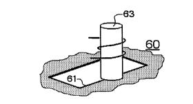
0 Figure 4 shows the principle of the register error determin~tion.
Considering one of the edges 61 of window 60, it can be seen that roughly 3
positions are possible with regard to the inductive sensor core. In figure 4-a,
core 62 lies entirely over a non-plated portion, so the current induced in the
metal layer is lowest; therefore the voltage at the oscillator termin~l~ will bes the greatest. Figure 4-b shows a position where core 63 lies partially over a
plated region and partially over a window; in this case some loading occurs
and, therefore, the oscillation amplitude is sm~ller than before. Finally, in
figure 4-c, core 64 lies entirely over a metal-plated region. Oscillator coil
loading is the highest; hence, the voltage of the oscillations is the ~m~llest.
Through proper choice of window sizes and positions, as well
as positions of the corresponding inductive sensors it becomes possible to
detect deviations of the metal pattern plated on the card, either on the
longitudinal or in the transversal directions, as well as pattern rotation relative
to the axes of the card.
2s Obviously, the voltage values detected by the sensors will vary
according with the thickness of the metal layer on the card, thus requiring an
adequate software for interpretation of the values furnished by said register
sensors.
As before, m~ximllm and Illillilll~llll acceptable measured levels
must be previously determined through standard cards with known register
mi~m~tches. Those values will be stored in the computer's memory, to enable
rejection of cards in which said register errors exceed allowable deviation
from true position.
Although the invention has been described with base in a
3s specific embo~liment it becomes clear that variations and modifications may
be introducad without ovel~le~ing the scope of the inventive concept. Thus,
for example, all data processing can be made by the device's CPU 21,
CA 02232162 1998-03-16
WO 97/11332 PCTABR96/00041
provided that enough memory is available and all necessary software is
loaded, elimin~tin~, therefore, the need for the use of micro-computer 11.
Moreover, although the description shows a device designed to
test cards with 104 cells (100 credit cells and 4 for positioning/validity), it
s shall be understood that the principle of the invention is equally applicable to
cards with any amount of cells and even for measurement of thickness of
continuos metal layers applied over an insulating m~f~ri~l
-