Note: Descriptions are shown in the official language in which they were submitted.
CA 02232199 1998-03-16
TITLE OF THE INVENTION
POWER CONVERTER WITH VOLTAGE DRIVE SWITCHING ELEMENT
BACKGROUND OF THE INVENTION
The present invention relates to a power converter
with an insulated gate semiconductor device of a MOS
gate structure, for example MOS-FET, IGBT (Insulated
Gate Bipolar Transistor), IEGT (Injection Enhanced Gate
Transistor) as a voltage drive switching element.
There is available a voltage drive switching
element as a switching element used in a power
converter, for example an inverter which drives an
induction motor converting a direct current power to
an alternating current power other than a current drive
switching element such as a thyristor, a gate turn-off
thyristor (GTO) or transistor. As typical examples of
a voltage drive switch:ing element, there are named:
an insulated gate semiconductor device of a MOS gate
structure, for example MOS-FET, IGBT (Insulated Gate
Bipolar Transistor), IEGT (Injection Enhanced Gate
Transistor).
FIG.1 shows a gate drive circuit of IGBT in a
conventional power converter. In FIG. l, if a switching
command vin for placing IGBT 7 in the conductive state
(on) or non-conductive state (off), a gate voltage Vge
corresponding to the switching command vin is applied
between the gate and emitter of the IGBT 7 through
transistors 3, 4 and a gate resistor 6. Thereby a
CA 02232199 1998-03-16
switching operation such as turn-on or turn-off is
performed in the IGBT '7. That is, if a positive
switching command vin :is input from a gate control
circuit not shown as shown in FIG. 2, the transistor 3
is placed in the on state and the transistor 4 is
placed in the off state, the output voltage vg becomes
a positive voltage and a gate voltage Vge which is
given through a gate resistor 6 is biased to the
positive side to turn on the IGBT 7. If the switching
command vin is negative, the transistor 3 is placed in
the off state, the transistor 4 is placed in the on
state, the gate voltage vg becomes a negative voltage
and the gate voltage is biased to the negative side to
turn off the IGBT 7.
A gate power supply for a forward bias (voltage
Ep) 1 and a gate power supply for a negative bias
(voltage En) 2 are respectively connected to the
transistors 3, 4 throuyh a limiting resistor 5.
In this case, the limiting resistor 5 is connected
between the gate power supply 2 and the transistor 4 or
to both of them.
IGBT has equivalent capacitances Cge 8, Ccg 9, Cce
10 and the like among the gate, emitter and collector
terminals as shown in FIG. 3. For this reason, a short
state arises between the collector and emitter in a
high frequency condition. Ccg + Cge is present as an
input capacitance Cies between the gate and emitter
CA 02232199 1998-03-16
of the IGBT. Therefore, in order to make IGBT effect
a switching operation, it is required charge and
discharge in the input capacitance Cies through a gate
resistor 6.
In a conventional gate drive circuit shown in
FIG. 1, there arises a delay in time constant (R6-Cies)
which is determined by the gate resistor 6 and the
input capacitance Cies, which sometimes causes a
trouble in the switching operation of the IGBT.
In order to make such a delay in time constant
smaller, it is considered that a value of a gate
resistance is made to be smaller or a voltage En of the
gate power supply 2 which gives a negative bias is made
to be higher.
However, when a value of the gate resistance 6 is
made to smaller, a turn-off speed of the IGBT 7 becomes
larger and a surge volt.age becomes higher and thus the
IGBT has a risk to have a damage by an overvoltage.
When a voltage En of the gate power supply 2 is biased
higher, a similar problem happens as well.
A current drive switching element and a voltage
switching element will be considered as a switching
element used in a power converter.
A turn-off charact.eristic of a current drive
switching element, such as GTO in general is that when
a load current is smaller, a turn-off time is shorter
but when the load current is larger, the turn-off time
CA 02232199 1998-03-16
is longer due to an influence of an accumulated charge
in a semiconductor elernent as shown in FIG 4. There-
fore, in a power converter such as an inverter in which
a current drive switching element is used, an on-gate
supply inhibiting time (which is called as a dead time)
to respective semiconductor elements of the positive
and negative arms is relatively taken long and longer
than the maximum turn-off time in consideration of the
maximum turn-off time when the maximum current of the
element is turned off and thereby short-circuit between
the positive and negative arms (direct current short)
is prevented.
On the other hand r it has actually observed that
a turn-off characteristic of a voltage drive switching
element such as an insulted gate switching element
is an absolutely inverse characteristic to that of a
current drive semiconductor switching element as shown
in FIG. 5, that is a characteristic when a load current
is larger, a turn-off t.ime is shorter, but when the
load current is smaller, the turn-off time is longer.
The reason why is that, as shown in FIG. 6, since
a capacitance of a gate is larger when a voltage
between a collector and emitter is smaller (such as in
the on state of the device), but a capacitance of a
gate is smaller (largely changed with two orders in
magnitude) when a voltage between a collector and
emitter is larger, charge to a gate capacitance from
CA 02232199 1998-03-16
the collector side is slowed if a load current is very
small.
For this reason, in an insulated gate switching
element, it is only required in order to prevent short-
circuit (direct current; short-circuit) between the
positive and negative arms that a dead time for the
positive and negative arms is set longer in considera-
tion of a turn-off time when a very small current of
the element is turned off. However, in that case, a
feature of an insulatecl gate switching element having a
high speed switching characteristic cannot be utilized.
While a higher switching frequency is desired in order
to make a load current assume a sine wave form, perfect
as much as possible in the case of PWM inverter and the
like, the upper limit of frequency is restricted due to
the restriction on the dead time.
BRIEF SUM~RY OF THE INVENTION
It is an object to provide a power converter
having a gate drive circuit effecting turn-off control
of a voltage drive switching element in a stable manner
by reducing a delay of a gate voltage of the voltage
drive switching element.
It is another object to provide a power converter
having a gate drive circuit which can utilize a high
frequency operation which a voltage drive switching
element has and performs a switching operation in a
stable manner in the range of a zero current to a rated
CA 02232199 1998-03-16
load current.
It is a further o:bject to provide a power
converter using a voltage drive switching element,
which realizes an operation with high reliability.
It is a still fur-ther object to provide a
pressure-welded insulated-gate switching element which
is preferably used as a voltage drive switching element
applicable to a power converter.
The present inven~ion discloses a device which
follows the following principles in order to achieve
the above mentioned ob-jects.
A concept of the present invention is a power
converter having at least a pair of voltage drive
switching elements, which comprises a gate control
circuit, the gate control circuit comprising:
detecting means for detecting at least one of
a set of device paramet.ers and a set of electric
parameters of the voltage drive switching elements;
monitoring means f.or monitoring at least one of
states of turn-on and turn-off of the voltage drive
switching elements based on the at least one of a set
of device parameters and a set of electric parameters
of the voltage drive switching elements detected by the
detecting means; and
control means for controlling a gate of the
voltage drive switching elements based on a monitoring
result of the monitoring means.
CA 02232199 1998-03-16
A first principle of the present invention
following the above mentioned concept has the above
mentioned gate control circuit as a feature, the gate
control circuit comprising:
deciding means for deciding completion of turn-off
of the voltage drive switching elements based on a gate
voltage of the voltage drive switching elements; and
bias shift means ior shifting a gate voltage of
the voltage drive switching elements to the negative
side when the decidiny means decides completion of
turn-off of the voltage drive switching elements.
A second principle of the present invention
following the above men.tioned concept has the above
mentioned gate control circuit as a feature, the gate
control circuit comprising:
detecting means for detecting a current flowing in
the pair of voltage drive switching elements; and
control means for controlling so as to decrease
a dead time till an on-gate signal is supplied to one
voltage drive switching element of the pair of voltage
drive switching elements and the other thereof after
the other voltage drive switching element is turned off
when a detected current detected by the detecting means
is larger than a predetermined value or to increase the
dead time till an on-gate signal is supplied to the one
voltage drive switching element of the pair of voltage
drive switching after the other voltage drive switching
CA 02232199 1998-03-16
-- 8
element is turned off when the detected current is
smaller than the predetermined value.
A third principle of the present invention
following the above mentioned concept has the gate
control circuit as a feature, the gate control circuit
further comprising:
self protecting means for performing a protecting
operation associated with a current flowing in a
voltage drive switching element;
self holding means for holding the protecting
operation when the self protecting means is activated;
and
reset means for resetting holding of a protecting
operation by the self holding means based on an
external signal.
A fourth principle of the present invention
following the above mentioned concept has the voltage
drive switching element as a feature, the voltage drive
switching element comprising:
an electrode pressure-welded to a voltage derive
switching element; and
an inductance element formed in the shape having
features of a cylinder and a spiral, which is provided
between an end of the voltage drive switching element
and the electrode.
Additional objects and advantages of the invention
will be set forth in the description which follows, and
CA 02232199 1998-03-16
in part will be obvious from the description, or may
be learned by practice of the invention. The objects
and advantages of the invention may be realized and
obtained by means of the instrumentalities and combina-
tions particularly pointed out in the appended claims.
BRIEF DESCRIPTION OF THE SEVERAL VIEWS OF THE DRAWING
The accompanying drawings, which are incorporated
in and constitute a part of the specification, illust-
rate presently preferred embodiments of the invention,
and together with the qeneral description given above
and the detailed description of the preferred embodi-
ments given below, serve to explain the principles of
the invention.
FIG. 1 is a diagram showing a structure of
a conventional power converter;
FIG. 2 is a wave form diagram for illustrating
operations of a conventional power converter;
FIG. 3 is a diagram showing equivalent
capacitances of IGBT;
FIG. 4 is a graph showing a turn-off characteris-
tic of GTO;
FIG. 5 is a graph showing a turn-off characteris-
tic of a voltage drive semiconductor element;
FIG. 6 is a graph illustrating a capacitance and
a voltage of the voltage drive semiconductor element
shown in FIG. 5;
FIG. 7 is a diagram showing a structure of a first
CA 02232199 1998-03-16
- 10
preferred embodiment of the present invention;
FIG. 8 is a diagram showing a wave form for
illustrating operations of the first embodiment of
the present invention in FIG.7;
FIG. 9 is a diagram showing a structure of
a second embodiment of the present invention;
FIG. 10 is a diagram showing a wave form for
illustrating operations of the second embodiment of
the present invention in FIG. 9 ;
FIG. 11 is a diagram showing a structure of
a third embodiment of t.he present invention;
FIG. 12 is a diagram showing a wave form for
illustrating operations of the third embodiment of
the present invention i.n FIG. 11;
FIG. 13 is a diagram showing a structure of
a fourth embodiment of the present invention;
FIG. 14 is a diagram showing a wave form for
illustrating operations of the fourth embodiment of
the present invention in FIG. 13 ;
FIG. 15 is a block. diagram showing an outline of
a structure of a fifth embodiment of the present
invention;
FIG. 16 is a circuit diagram showing a level
discriminating circuit of the fifth embodiment shown in
FIG. 15;
FIG. 17 is a block: diagram showing a structure of
a sixth embodiment of the present invention;
CA 02232199 1998-03-16
FIG. 18 is a block diagram showing a structure of
a seventh embodiment of the present invention;
FIG. 19 is a diagram showing a structure of
a eighth embodiment of the present invention;
FIG. 20 is a diagram showing operations of
the semiconductor element shown in FIG. 19;
FIG. 21 is a bloc~; diagram showing a structure of
a ninth embodiment of the present invention;
FIG. 22 is a block diagram showing an outline of
a structure of a tenth embodiment of the present
invention;
FIGS. 23A to 23D are operation wave forms showing
operations of self-protecting means and self-holding
means shown in FIG. 22;
FIG.S. 24A to 24C are operation wave forms showing
operations of self-protecting means and self-holding
means shown in FIG. 22;
FIG. 25 is a block diagram showing an outline of
a structure of a eleventh embodiment of the present
invention;
FIG. 26 is a block diagram showing an outline of
a structure of a twelfth embodiment of the present
invention;
FIG. 27 is a block diagram showing an outline of
a structure of a switching element of a power converter
in a thirteenth embodiment of the present invention;
FIGS. 28A and 28B are a table and a graph showing
CA 02232199 1998-03-16
a relation between an operation of self-holding means
and current restriction of power converter of a four-
teenth embodiment of the present invention;
FIGS. 29A to 29C are a table and graphs showing
a relation between an operation of self-holding means
current restriction of power converter of a fifteenth
embodiment of the present invention;
FIG. 30 is a view partially in section of a
package of a flat type IEGT of a sixteenth embodiment
of the present invention;
FIG. 31 is a sectional view taken on line
XXXI - XXXI of FIG. 30;
FIG. 32 is a perspective view of a coil in the
shape of a cylinder shown in FIG.30;
15FIG. 33 is a perspective view of a coil in the
shape of a quadrangular prism shown in FIG.30;
FIG. 34 is a sectional view along a central line
of the coils shown in FIGS. 32 and 33;
FIG. 35 is a perspective view of the coil in the
20shape of a cylinder shown in FIG. 30, which is applied
with an insulating coating; and
FIG. 36 is a sectional view along a central line
of the coil shown in FIG. 35.
DETAILED DESCl~IPTION OF THE INVENTION
25A concept of the present invention is that at
least one of the turn-on and turn-off states of voltage
drive switching elements is monitored based on at least
CA 02232199 1998-03-16
one of a set of device parameters and a set of electric
parameters of a voltage drive switching element, and
a gate of the voltage drive switching elements is
controlled based on the monitoring results. Herein,
the device parameters c~nd electric parameters are those
associated with a device, a gate, a emitter and a
collector of the element.
A first principle of the present invention
following the concept is that completion of turn-off of
a voltage drive switch:ing element is decided based on a
gate voltage of the vo:Ltage drive switching element and
the gate voltage of the voltage drive switching element
is shifted to the negat;ive bias side when it is decided
that turn-off is completed.
Thereby, a delay of the gate voltage of the
voltage drive switching element is reduced and turn-off
control of the voltage drive switching element can be
performed in a stable manner.
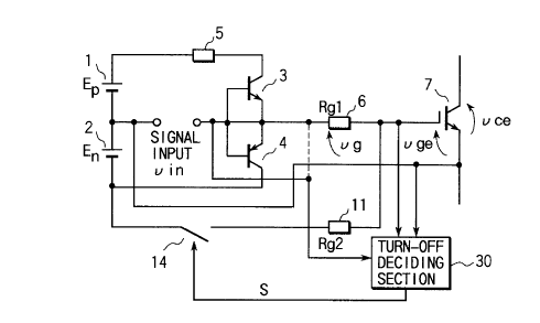
A first preferred embodiment following the first
principle of the present invention will be described in
reference to FIG. 7. As shown in FIG. 7, in a gate
drive circuit of a power converter of the embodiment,
a second gate resistor 11 is connected between the
gate of IGBT 11 of a switching element of the power
converter through a switch 14. The switch 14 is
operated into the ON or OFF states based on a decision
signal S and a negative voltage (- En) is applied to
CA 02232l99 l998-03-l6
- 14
the second gate resistor 11 by the OFF state of the
switch 14. A decision signal S given to the switch 14
is supplied from a turn-off deciding section 30 which
decides completion of turn-off of IGBT 7 based on a
voltage Vge between the gate and emitter of the IGBT 7.
The other constituents are the same as those of the
conventional circuit of FIG. 1 and the same marks are
given.
In the above ment.ioned structure, if a switching
command vin of a positive or negative voltage is input
from a gate control circuit not shown, the same
switching operation as done conventionally is conducted.
That is, if a switching command vin of a positive or
negative voltage is given, a voltage vg corresponding
to the switching command vin is output through a
transistor 3 or 4, a gate voltage, positive or negative,
is applied between the gate and emitter of the IGBT 7
through a gate resistor 6. Thereby, the IGBT 7 is
turned on or off. The switching operation is the same
as done conventionally.
In this case, if a switching command vin of a
negative voltage is input~ the transistor 4 becomes
conductive and a voltage vg corresponding to a negative
voltage of a gate power supply 2 is output, the IGBT 7
starts a turn-off operation. At this point, a voltage
vg between a gate and emitter is kept at a level called
a Miller voltage (generally on the order of 5V) till a
CA 02232199 1998-03-16
current flowing into a collector is changed to zero as
shown in FIG. 8 by a turn-off characteristic of IGBT 7.
When the current is zero, the voltage is rapidly
transferred to a negatively biased state. In the
turn-off, since a collector current is reduced at a
predetermined current change rate di/dt, as a breaking
current is larger, a generating time of a Miller
voltage lasts longer and as a breaking current is
smaller, a generating time of the Miller voltage lasts
shorter as indicated by a dotted line.
When the gate voltage vge is transferred to a
negatively biased state, a decision signal S of
completion of turn-off is output from a turn-off
deciding section 30 and a switch 14 is in the
conductive state and a negative voltage (-En) of the
gate power supply 2 is supplied between the gate and
emitter of the IGBT 7 in parallel through a second gate
resistor 11.
Thereby, the gate voltage vge is rapidly shifted
and biased to the negative side. Therefore, a voltage
between the collector and emitter of the IGBT 7 is
rapidly raised and if a large dv/dt is applied, the
IGBT 7 is not again ignited and can keep its turn-off
state and thus the IGBT 7 can complete a turn-off
operation in a stable manner.
FIG. 9 shows a second embodiment of a gate drive
circuit of the present invention in a concrete manner.
CA 02232l99 l998-03-l6
- 16
The gate drive circuit comprises: as shown in FIG. 9,
transistors 12, 13, 14, resistors 15, 16, 17 and a
diode 18. The other constituents are the same as the
conventional circuit iII FIG. 1 and the same marks are
used.
In the structure of FIG. 9, if a switching command
vin of a negative voltage is input from a gate control
circuit not shown, a transistor 3 is placed in the
off state, a transistor 4 is placed in the on state,
a voltage of - En is input to a gate resistor 6,
a transistor 12 is placed in the off state and transis-
tors 13 and 14 are placed in the on state. Thereby a
voltage of - En is input to a second gate resistance 11
and a gate voltage Vge from the second gate resistor 11
is supplied to the IGBT 7 in parallel to a gate voltage
Vge supplied from the gate resistor 6.
In this situation, when the switching command vin
is changed to a positive voltage, the transistor 4 is
placed in the off state but the transistor 3 is placed
in the on state and an input voltage vg of the gate
resistor 6 is from - En to + Ep. At the same time, the
transistor 12 is change to be placed in the on state
from the previous off state and the transistor 14 is
placed in the off state and an input voltage of the
second gate resistor 11 is changed from - En to a zero
voltage and thus a reference gate voltage Vge is
started to change in a positive direction at a change
CA 02232199 1998-03-16
rate of time constant liR6-Cies)~
At the time point when the gate voltage Vge is
changed from the negative side to positive side, the
transistor 13 is placecl in the off state and a gate
voltage Vge is increased, so that the IGBT is
controlled to be in a t:urn-on state.
Thereafter, when a switching command vin is
changed from a positive voltage to a negative voltage
in a condition in which a current flows in the
collector of the IGBT 7, a transistor 3 is placed in
the off state and the transistor 4 is placed in the on
state. Thereby, a voltage of - En is input to a gate
resistor 6 and at the same time a transistor 12 enters
the off state.
However, when a current flows in the collector of
the IGBT 7, as shown in FIG. 10, a voltage Vge between
the gate and emitter does not immediately change to
a negative voltage but is kept at a Miller voltage as
mentioned above. For this reason, the transistor 13 is
not immediately transited to the on state but a base
current does not flow in the transistor 14 and the
transistor 14 is kept in the off state even if the
transistor 12 is in the off state.
Therefore, the IGBT 7 is subjected to turn-off
control only by the gate voltage Vge supplied from
the gate resistor 6. When the collector current is
reduced to zero and the Miller voltage disappears and
CA 02232199 1998-03-16
- 18
a gate emitter voltage Vge is negative, the transistor
13 is placed in the on state and the transistor 14 is
also placed in the on state and a voltage input to the
second gate resistor 1] changes from a zero voltage to
- En. Thereby, a negat:ive gate voltage Vge is in
parallel supplied to the IGBT 7 from the gate resistor
6 and the second gate resistor 11.
Therefore, according to the embodiment, after the
IGBT 7 completes a turn-off operation, the gate voltage
vgt is rapidly biased to the negative side at a time
constant [Cge-(Rg1-Rg2)/( Rg1 + Rg2)] shorter than an
conventional example (FIG. 1) indicated by a dotted
line. Thereby, a second ignition by a collector-emitter
voltage dv/dt of the IGBT 7 can be prevented from
occurring.
In the embodiment, since completion of turn-off of
the IGBT 7 is detected and thereby the gate voltage is
controlled, a change in characteristic by a breaking
current or a dispersion by difference between devices
do not affect the effect.
FIG. 11 shows a third embodiment of a gate drive
circuit. In FIG. 11, a gate drive circuit of the
embodiment further comprises: diodes 19, 20 and
resistors 21, 22 in addition to those included in
FIGS. 9 and 1.
In the embodiment, the transistor 13 is brought in
the on or off state by a voltage vge on the output side
CA 02232199 1998-03-16
-- 19
or a voltage on the input side of the gate resistor 6,
whichever is higher. In the structure of FIG. 11, if
a switching command vir, of a negative voltage is input
from a gate control circuit not shown, the transistor 3
is placed in the off state and the transistor 4 is
placed in the on state. Thereby, a voltage of - En is
input to the gate resistor 6 and the transistors 13, 14
are both placed in the on state and a voltage of - En
is input to the second gate resistor 11. A negative
gate voltage Vge is supplied in parallel to the IGBT 7.
When the switchinq command vin changes to a
positive voltage from this situation, the transistor 4
enters the off state but the transistor 3 enters the on
state. In company with this, an input voltage vg of
the gate resistor 6 changes from - En to + Ep. At the
same time, the transistor 13 changes its state from on
to off and the transistor 14 enters the off state and
as a result an input side of the second gate resistor
ll assumes the open state. Thereby, The gate voltage
Vge increases in the positive direction at a change
rate of a time constant (R6-Cies) and the IGBT 7 is
controlled to be in a turn-on state shown in FIG 12.
Thereafter, when the switching command vin changes
to a negative voltage in a condition in which a current
flows in the collector of the IGBT 7, the transistor 3
is again placed in the off state, the transistor 4 is
placed in the on state and a voltage of - En is input
CA 02232199 1998-03-16
- 20
to the gate resistor 6.
However, since if a current flows in the collector
of the IGBT 7, a gate emitter voltage Vge is not immedi-
ately changed to a negative voltage but kept at a
Miller voltage, the transistor 13 does not immediately
enter the on state and the off state of the transistor
14 is kept as shown in FIG. 12.
Therefore, the IGE3T 7 is subject to turn-off
control only by the gat.e voltage Vge supplied from the
gate resistor 6. When a collector current is changed
to zero and the miller voltage disappears and the gate
voltage Vge changes to be negative, the transistor 13
is brought in the on state and the transistor 14 also
obtains the on state. Thereby, a voltage input to the
lS second gate resistor 11 changes from zero to - En and
thus a negative gate voltage Vge is supplied to the
IGBT 7 from the gate resistor 6 and the second gate
resistor 11 in a parallel manner.
As can be seen from the above description,
according to the present invention, after the IGBT
completes a turn-off operation, the gate voltage Vge
is rapidly shifted and biased to the negative side in
a similar way to that in the already mentioned embodi-
ments and thereby a second ignition of the IGBT 7 by
increase of dv/dt of a collector emitter voltage can be
prevented from occurrenre.
FIG. 13 shows a fourth embodiment of a gate drive
CA 02232199 1998-03-16
circuit of the present invention in a concrete manner.
A gate drive circuit shown in FIG. 13 has a structure
which comprises diodes 23, 24 in addition to the
circuit shown in FIGS. 1 and 11.
In a gate drive circuit of the embodiment, when a
switching command vin is given with a negative voltage,
a input voltage vg of a gate resistor 6 is made to be a
zero voltage to make the gate and emitter of the IGBT 7
short therebetween through the gate resistor 6.
In the embodiment, if the switching command vin
changes from a positive voltage to a negative voltage
in a condition in which the IGBT 7 assumes the on state
and a collector current flows, the IGBT 7 starts a
turn-off operation. Thereby, the gate voltage Vge is
kept at a Miller voltage, as described above. When the
collector current becomes zero and the Miller voltage
disappears, the gate voltage vge is reduced to a
negative voltage and a base voltage vO which is given
to the transistor 13 through a diode 20 and a resistor
17 becomes negative. For this reason, as shown in
FIG. 14, the transistor 13 assumes the on state and the
transistor 14 also assumes the on state and a voltage
of - En is applied to the second gate resistor 11.
Thereby, the gate voltage vge is rapidly biased to the
negative side and a second ignition of IGBT 7 by dv/dt
of a collector-emitter voltage is prevented from
occurrence.
CA 02232199 1998-03-16
According to the embodiment, since a turn-off
operation of the IGBT .7 is made to perform in a
relatively slow pace to control a surge voltage by
di/dt and thereby the gate voltage Vge can be rapidly
biased to the negative side from a time point when
turn-off is completed, a second ignition of the IGBT 7
by dv/dt of a collector emitter voltage can be prevented
from occurrence.
The diode 24 is used to prevent application of an
excessively large reverse voltage between the collector
and emitter of the transistor 4.
As described above, according to the gate drive
circuit of a voltage drive switching element of the
present invention, since when the voltage drive
switching element compl.etes a turn-off operation, the
gate voltage can rapidly be shifted to a negatively
biased side and thereby an erratic ignition caused by
dv/dt of a main circuit. is prevented and switching
control on on/off with stability and high reliability
can be performed.
An embodiment following the second concept of
the present invention will be described. The second
concept of the present invention is that control is
performed in such a manner that a current flows in a
pair of voltage drive switching elements is detected,
if the detected current is equal to or larger than a
predetermined value, a dead time till an on-gate signal
CA 02232199 1998-03-16
is supplied to one of t;he pair of voltage switching
elements after the other of the pair of voltage drive
switching elements is t:urned off is shorten and if the
detected current is less than the predetermined value,
a dead time till an on-gate signal is supplied to the
one of the pair of volt:age switching elements after the
other of the pair of voltage drive switching elements
is turned off is longer.
Thereby, a high frequency operation which a
switching element has can be utilized and a switching
operation from a zero current to a rated load current
can be performed in a stable manner.
A fifth preferred embodiment following the second
concept of the present invention will be described in
reference to FIGS. 15, 16. As shown in FIG. 15, a main
circuit of a power converter of the present invention
comprises: a direct current power supply 101; insulated
gate semiconductor elements in series connected
therebetween 111 to 114, diodes llla to 114a in inverse
parallel connected to respective elements 111 to 114.
The main circuit of the power converter can output
a alternating power by arms of two sets or more of
insulated gate semiconductor elements 111 to 114 and
diodes llla to 114a in reverse parallel connected to
the devices, wherein one set of insulated gate elements
111 to 114 and diodes llla to 114a are called one arm.
A control circuit of the power converter
CA 02232199 1998-03-16
_ 24
comprises: current transformers 121 to 124 provided
for each arm; a level cliscriminating circuit 131 for
discriminating an output level or a polarity of each
current transformer; a control circuit, for example
a voltage frequency (V~'F) control circuit 132, for
supplying an on or off signal to each of elements 111
to 114; a dead time control circuit 133; a gate pulse
distributor 134; and a gate drive circuit 135.
The level discriminating circuit 131 discriminates
an output level of the current transformers 121 to 124
provided to each arm. A dead time which is set in the
dead time control circuit 133 is switched based on an
output signal of the level discriminating circuit 131.
That is, when an arm current is smaller than a prede-
termined value, a dead time is adjusted to be longer
and when the arm current is larger than the predeter-
mined value, the dead t,ime is adjusted to be smaller.
As shown in FIG. ]6, in the level discriminating
circuit 131, two photo-couplers PHl are provided at the
secondary side of a current transformer 121 provided
for each arm in parallel with an inverse polarity and A
and B signals are obtained based on whether a current
flows in the positive c,r negative direction and an
output level of the main circuit is discriminated by
the A and B signals.
A sixth embodiment, of the present invention is
shown in FIG. 17. As shown in FIG. 17, a power
CA 02232l99 l998-03-l6
- 25
converter comprises: a direct current power supply 101;
insulated gate semiconductor elements 111 to 114; and
diodes llla to 114a in inverse parallel connected to
respective elements 111 to 114. In the power converter,
an alternating current output can be obtained using two
arms or more of devices and diodes, wherein one arm
comprises elements 111 to 114 and diodes llla to 114a
in combination.
A control circuit of the power converter
comprises: a current transformer 125 for detecting a
direct current; a level discriminating circuit 131 for
discriminating an output level of the current tans
former 125; a V/F control circuit 132 for supplying
an on or off signal to each of the elements 111 to 114;
a dead time control circuit 133; a gate distributor
13 4; and a gate drive circuit 13 5.
The level discriminating circuit 131 discriminates
an output level of the current transformer 125 provided
for detecting a direct current. A dead time which is
set in the gate control circuit is switched based on an
output signal of the level discriminating circuit 131.
That is, when a direct current is smaller than a prede-
termined value, a dead -time is adjusted to be longer
and when the direct cur:rent is larger than the prede-
termined value, the deacl time is adjusted to be smaller.
A seventh embodiment of the present invention will
be described in reference to FIG. 18. In FIG. 18, the
CA 02232l99 l998-03-l6
- 26
same marks as those in FIGS. 15, 16 indicate the same
constituents and what is different from FIGS. 15, 16 is
only to a current transformer 126 is provided in an
output line. That is, a dead time which is set in the
dead time control circuit 133 is switched based on an
output signal of the level discriminating circuit 131.
That is, it is controlled in such a manner that when
a direct current is smaller than a predetermined value,
a dead time is adjustecl be longer and when the direct
current is larger than the predetermined value, the
dead time is adjusted to be smaller.
An eighth embodiment of the present invention will
be described in reference to FIG. 19. In FIG. 19, the
same marks as those of FIGS. 15, 16 indicate the same
constituents and only two arms of a current transformer
are shown. In FIG. 19, an light emitting device 140,
such as a photo-coupler as means for detecting a
negative bias between the gate and emitter of elements
111, 112 is provided and it is detected based on the
light detection signal that the elements 111, 112 have
actually turned off. Gate signals GA, GB are supplied
to the elements 111, 112 the pair of arms through AND
circuits AND 1, AND 2 for obtaining a conjugation of
the signals X, Y and gate signals A, B of a pair of
arms, and amplifiers AMP1, AMP2.
FIG. 20 shows a collector voltage VCE and
a collector current IC when a element is turned off,
CA 02232199 1998-03-16
a collector current IC and a voltage between the gate
and emitter VGE. When a relatively large current is
cut off, a gate signal as in the shape of a wave
depicted by a solid line is supplied and thereby a
miller voltage is generated and immediately thereafter
a negative voltage appears. On the other hand, it has
been found that when a very small current is cut off, a
wave form in the shape depicted by a dotted line which
has a mild slope is supplied and thereby a turn-off
time takes more than double.
In FIG. 19, since a negative bias voltage is
generated between the gate and emitter as shown in
FIG. 20 when a element is turned off and a current is
zero, a current flows in a light emitting element 140
by the negative bias voltage. Thereby, it is detected
that the element is turned off, a conjugation of the
detected signal and an on-gate command of a pair of
the element is obtained and a gate signal is output.
Thereby, since it is prevented that negative and
positive arms assume the on state at the same time,
generation of direct current short-circuit can be
prevented from occurrence even when a turn-of time of
the device changes.
A ninth embodiment of the present invention will
be described in reference to FIG. 21. That is, in
FIG. 21, the same marks as those in FIG. l9 indicate
the same constituents and a current detector 150 for
CA 02232199 1998-03-16
detecting a negative gate current when the element is
turned off and a flip-flop circuit 151 which is
operated by the signal of the detector 150 are
provided.
The current detector 150 detects a positive
current while an off-gate current flows in one element
111 and thereby the current detector 150 gives a signal
to the flip-flop circui.t 150 so that an on-gate signal
is not supplied to one element 111 the other element
112 of the pair. Thereby, the flip-flop circuit 151 is
reset. On the other hand, the current detector 150
supplies a signal to the flip-flop circuit 151 in order
to set the flip-flop circuit 151 when the current
detector 150 detects a negative gate current. A signal
a of the flip-flop circuit 151 corresponding to the one
device 111 and a signal a of the flip-flop circuit 151
corresponding to the other element 112 of the pair are
combined to generate a conjugation by an AND circuit
ANDl and an output of the AND circuit AND1 is given to
the device 111 as a gate signal GA through an amplifier
AMP7 and a resistor 7.
In such a structure, since it can be prevented
that positive and negative arms assume the on states at
the same time using an output signal of the current
detector 150 by the same operations as those in the
above mentioned embodiments, generation of direct
current short-circuit is prevented even when a turn-off
CA 02232199 1998-03-16
time of the device changes.
As seen from the above description, according to
the present invention, since detecting means for
detecting a current flowing in a semiconductor device
and its polarity is provided, it is controlled based
on a result of the detecting means in such a manner
that a dead time of positive and negative arms of the
converter is adjusted t.o last longer when the detected
current is smaller than a predetermined value or the
dead time is adjusted t.o last shorter when the detected
current is larger than the predetermined value, even
though the semiconductor device has a turn-off charac-
teristic which is peculiar to the device, that is, a
turn-off time is shorter when a current is larger but
the turn-off time is longer when the load current is
smaller and thereby a high frequency operation of the
semiconductor device can be utilized, so that there can
be provided a power converter having a gate drive
system which can be driven in a stable manner in the
range of a zero current to a rated load current with
high reliability.
A third principle of the present invention
following the above mentioned concept will be described.
The third principle is that a protecting operation is
held when self protecting means for performing a
protecting operation associated with a current flowing
in a voltage drive switching element operates and
CA 02232199 1998-03-16
- 30
holding of the protecting operation by the self
protecting means is reset by an external signal.
Thereby, a power converter using a voltage drive
switching element, which realizes an operation with
high reliability can be provided.
An preferred tenth embodiment following the third
principle of the present invention will be described
in reference to FIG, 22. In the preferred embodiment
following third principle, as a switching element of a
power converter, IPM (Intelligent Power Module) having
self protecting means is used.
In FIG. 22, IPM 226 which is a switching element
of the power converter comprises IGBT element 217 to
which a diode 218 is inversely connected. A gate drive
device 225 is connected to the gate of the IGBT element
217. IPM 226 comprises an overcurrent protecting
circuit 220 for overcurrent protection of the IGBT
element 217 and a short-circuit current protecting
circuit 221 for short-circuit current protection. The
IPM 226 receives outputs of the overcurrent protecting
circuit 220 and the short-circuit current protecting
circuit 221 and has a fault detector 214 for protecting
fault detection of the IGBT element 217. In addition,
the IPM comprises a self holding circuit 227, an output
signal terminal 271 of -the self holding circuit and
a reset signal terminal 272 of the self holding circuit
227, which are characteristic part of the embodiment.
CA 02232199 1998-03-16
In such a structure, as a self protecting function
of the IGBT element 217, there are provided the
overcurrent protecting circuit 220 and the short-
circuit current protect;ing circuit 221. When these
circuits 220, 221 operate, a protecting operation is
performed by stopping a gate control signal which is
supplied to the IGBT element 217 from the gate drive
circuit 225 and at the same time a operation signal is
supplied to the self holding circuit 227. In the fault
detector 224, operations of these protecting circuits
may be detected and a signal of the output signal
terminal 271 of the self holding circuit 227 may be
used. The self protect.ing circuit 227 self holds a
protecting operation till the circuit 227 is reset by
an input signal of the reset signal terminal 272 and a
signal is also supplied. to the gate drive circuit 225
during this self holding period.
~elations between operations of the overcurrent
protecting circuit 220 as self protecting means
associated with a current in the IGBT element 217 of
FIG. 22 or the short-circuit current protecting circuit
221 and an operation of the self holding circuit are
described in reference to FIGS. 23A to 23D and
FIGS. 24A to 24C. FIGS. 23A shows a wave form diagram
of a gate control signal supplied to the IGBT element
217 through the gate drive circuit 225, FIG. 23B shows
a wave form diagram of a protection output control
CA 02232199 1998-03-16
- 32
signal of the short-circuit current protecting circuit
221, FIG. 23C shows a wave form diagram of an output
signal of the self holcling circuit 227 and FIG. 23D
shows a wave form of a reset signal supplied to the
self holding circuit 227 from the reset signal
terminal 272.
In FIGS. 23A to 23D, the IGBT element 217 normally
operates by receiving a gate control signal till time
tl, in accompany with an operation of the protecting
circuit the self holding circuit 227 is actuated and
continues self holding when the short-circuit current
protecting circuit 221 is activated at time tl and a
reset signal is normally supplied from the reset signal
terminal 272 to reset the self protecting circuit at
time t2, so that a gate control signal is supplied to
the IGBT element 217. In such a manner, the IPM 226
which is a semiconductor device shown in FIG 22 can
self-hold an operation of the self protecting circuit
by the self holding circuit 227 till a reset signal is
supplied from the outside of the IPM 226.
FIG, 24A is a wave form diagram of a gate control
signal supplied to the IGBT element 217 through the
gate drive circuit 225, FIG. 24B is a wave form diagram
of a protection output signal of the short-circuit
current protecting circuit 221 and FIG. 24C is a wave
form of an output signal of the self holding circuit
227. In FIGS. 23A to 23C, the self holding circuit 227
CA 02232199 1998-03-16
starts a self holding operation in company of
generation of protection output signal of the short-
circuit protecting circuit 221, whereas in FIGS. 24A
to 24C, the self holding circuit 227 starts at time t6
and continues the self holding after the number with
generation times of a protection output signal reaches
a predetermined number or a time interval in which
a protection output signal is generated elapses a
predetermined interval.
As shown in FIGS. 24A to 24C, IPM 2260f FIG. 22
only exerts self protection against a transitory
erratic ignition of an IGBT element 217, for example,
caused by a noise mixed into a gate control signal.
IPM 226 of FIG. 22 activates the self holding circuit
227 against phenomena which happens after a time t6,
and which should be countered by intrinsic self
protection, such as degradation of an IGBT element 217
caused by repetition of a transitory erratic ignition,
for example, and can continue a self holding operation
till a reset signal is supplied from the outside of
IPM 226.
An eleventh embodiment of the present invention
will be described in reference to FIG. 25. IPM 226'
which is a semiconductor device of FIG. 25 comprises:
a gate derive circuit 228, a gate resistor 229 and an
output signal terminal 273 of a self holding circuit in
addition to the constituents shown in FIG. 22.
CA 02232199 1998-03-16
- 34
In IPM 226' of the embodiment, there is shown
the case where four IGBT elements 217 each as a chip
in a device package ancl four diodes are connected in
parallel in an equivalent manner. While the number of
chips connected in parallel in a package is not limited,
the four IGBT elements 217 are accommodated and two of
them and the other two thereof are respectively
connected in parallel and supplied with a common gate
signal from the gate drive circuits 228 through the
gate resistors 229. Two sets of this combination are
in parallel connected i.n the package in an equivalent
manner and a parallel configuration of the four IGBT
elements 217 is complet.ed. For each unit of parallel
connection controlled by a common gate drive circuits
228, the overcurrent protecting circuit (OCC) 220 and
the short-circuit current protecting circuit (SCC) 221
are provided as a self protecting function associated
with a current.
The number of chips in parallel connected in an
equivalent manner is not specifically limited in a
package of the semiconductor device, a self protecting
function is provided for each predetermined parallel
connection unit in which constituents are in parallel
connected and thereby a self protecting operation can
independently be conducted in each of degraded parallel
connection units.
As shown in FIG. 25, since the self holding
CA 02232199 1998-03-16
circuit (SHC) 227 is provided for each parallel
connection unit, a plurality of self holding circuits
227 are provided in the package and a probability at
which all the chips in the package of the semiconductor
device are degraded at the same time is lower, only the
limited number of parallel connection units are brought
in a self protecting mode and the other parallel
connection units can continue a switching operation as
a semiconductor device with supply of a gate control
signal from the gate drive circuit 228 in a normal
manner.
In such a manner, even while the IPM 226'
continues its operation, an operational condition of
the self holding circuit 227 can be discriminated by
each of output signals from the output signal terminals
271, 273 of the self holding circuits 227.
In a semiconductor device of a MOS gate structure
such as the IGBT element 217, the gate drive circuit
228 has a high possibility for the case where the gate
terminal of the IGBT element 217 assumes a low input
impedance due to degradation of the gate terminal of
the IGBT element 217 wh.ich has conducted a self
protecting operation. .rn such a manner, if the gate
terminal has assumed a .low impedance, a signal level
on the input side of the gate drive circuit 228 is
affected. Thereby gate control signals of other
parallel connection uni1s of IGBT elements 217 which
CA 02232199 1998-03-16
have not conducted a self protecting operation can be
reduced. In order to prevent such an influence from
being exercised, a switching function can be provided
in the gate drive circuit 228 so that a gate control
signal is not supplied from the corresponding gate
drive circuit 228 during a period the self holding
circuit 227 of a parallel connection unit which has
conducted a self protecting operation continues a
self holding operation.. Thereby a self holding
operation can be made t:o continue without any external
disturbance acting on a gate control signal of orderly
parallel connection units or an orderly IPM 226' in
parallel connected externally.
A parallel conneclion unit in which a gate control
signal is not supplied by activating a switching
function of the gate drive circuit 228 may be operated
by the gate drive circuit 228 so that the gate terminal
and the emitter terminal of the IGBT element 217
assumes a short-circuit. condition in an equivalent
manner only during when the gate control signal is not
supplied.
A twelfth embodiment will be described in
reference to FIG. 26. That is, FIG. 26 shows a circuit
configuration in the case where IPM 226 which is a
semiconductor device, as shown in FIG. 22 ( or the IPM
226' shown in FIG. 25) is adopted as a switching
element of a power converter. In FIG. 26, the power
CA 02232l99 l998-03-l6
- 37
converter comprises a self protection monitoring
circuit 230 and a control circuit 231. When self
protecting means is act,ivated and thereby self holding
means is activated in t,he inside of the IPM 226 shown
in FIG. 22 (or the IPM 226' shown in FIG. 25), the self
protection monitoring circuit 230 detects this and
transmits the informati.on to the control circuit 231.
However, since the control circuit 231 operates so
that the control circui.t 231 continues to supply a gate
control signal to the IPM 226 in the scope of operation
of predetermined holding means, the power converter
using a semiconductor d.evice can continue its operation.
Therefore, operational reliability of a power
converter can be improved by a great margin, as
compared with a conventional power converter which
stops its operation imm.ediately after only one chip is
degraded.
A thirteenth embodiment of the present invention
will be described in reference to FIG. 27. In a
circuit shown in FIG. 27, three IPMs 226 (or three IPMs
226' shown in FIG. 25) which are semiconductor devices
are in parallel connected. Parallel connection of the
semiconductor devices can be made to operate as one
switching element 215 in an equivalent manner.
In the case where as shown in FIG. 27, the IPM 226
is in parallel connected and applied to as a switching
element of the power converter as shown in FIG. 26,
CA 02232l99 l998-03-l6
- 38
an operation of the power converter using the semicon-
ductor devices can continue while monitoring an
operational condition of self holding means, it is
detected by the self protection monitoring circuit 230
if self protecting means in the inside of the IPMs 226
in parallel connection is activated.
In the self protection monitoring circuit 230,
since an operational condition of the self holding
means is monitored, the monitoring circuit 230 outputs
a signal to the control circuit 231 in correspondence
to an operational situation of the self holding means
and thereby a current of the power converter is
controlled. When a current of the power converter
is controlled in correspondence to the operational
situation of the self holding means, the power
converter can be continued to operate while operational
reliability is improved with a margin in terms of
a magnitude of current since a current load on other
IPMs 226 in parallel connected is reduced.
A fourteenth embodiment of the present invention
will be described in reference to FIGS. 28A, 28B.
FIG. 28A shows the number of self holding means which
are in operation by six IPMs (switching elements) shown
in FIG. 26. FIG. 28A shows a limited value of a
current of the power converter. In FIGS. 28A, 28B, U
and X, V and Y, and W and Z are combinations of two
IPMs (switching elements) each in series connected with
CA 02232199 1998-03-16
- 39
each other and inserted between direct current buses.
While there is no operation of the self holding
leans till a time ta, after the time ta, the self
holding monitoring circuit 230 discriminates the
largest operational number of self holding functions
in comparison among the three sets of IPMs (switching
elements) in each set c,f which two IPMs are in parallel
connected and a current of the power converter is
controlled through the control circuit 231.
The limited value of a current is changed
sequentially at ta, tb and tc and in FIG. 28, the
operation of the power converter is terminated since
a total number of the IPMs (switching element) having
the same self holding functions amounts to four at a
time td.
In such a manner, if the power converter is made
to continue its operation under limitation of a current
while it is discriminated in which circuit portion a
self holding means is activated by the self holding
monitoring circuit 230 by the IPMs (switching elements),
operational reliability can greatly be improved,
compared with a conventional power converter. That is,
while a conventional power converter has stopped by
even only one self holding means in operation,
operational reliability of a power converter can be
improved by a rate corresponding to a continuous
operation till a total number of self holding means
CA 02232199 1998-03-16
- 40
reaches nine in the embodiment.
A fifteenth embodiment of the present invention
will be described in reference to FIGS. 29A to 29C.
FIG. 29A shows the number of self holding means which
are in operation by six IPMs (switching elements)
shown in FIG. 26. FIG. 29B shows a limited value of
a current of the power converter. FIG. 29C shows
a signal input to a reset signal terminal 272 of IPM
shown in FIG. 22 or FIG. 25.
While a operational situation of the self holding
means is monitored by the self holding monitoring
circuit 230 and a current of the power converter is
limited at times ta and tb in a similar manner to in
FIGS 28A to 28B, a reset signal is input to a reset
signal terminal 272 of the IPM 226, which is a
semiconductor device, from a control circuit 231 at a
time te. Since the reset signal is input to the reset
signal terminal of the IPM 226 at the time te, an
operation of the self holding means can be reset when
the operation is not ca-used by a factor of the IPM
itself but caused by a -temporary factor on the load
side. Thereby, if the self holding means can be reset,
a limited value of a current of the power converter is
changed after a time td when a reset signal is input
and thus operational reliability of the power converter
can be improved.
While in the above mentioned embodiments, IPM 226
CA 02232l99 l998-03-l6
_ 41
using an IGBT element 217 is employed, kinds and the
number are not limited to that. Kinds of self protect-
ing means provided in a semiconductor device is not
specifically limited, but any self protecting means can
be used as far as it at least corresponds to a current
factor and in addition the numbers of self protecting
means and self holding means in a semiconductor device
is also not restrictive. A power converter using a
semiconductor device is not specifically limited in
aspects of its circuit system or a restrictive method
of its current.
As mentioned above, according to the present
invention, a semiconductor device with which
operational reliability can be improved and a power
converter using the same can be provided.
In the third principle of the present invention,
a signal cannot be supplied from the drive circuit to
a predetermined chip during a period when self holding
means in operation in company with a protecting
operation of self protecting means.
At least when self protecting means is activated
in a predetermined semiconductor device, self holding
means corresponding to self protecting means which
has been activated can be made to operate, while an
operation is continued using a semiconductor device
whose self protecting means is not activated.
There can be provided a monitor detecting means
CA 02232199 1998-03-16
- 42
for monitoring and detecting self holding means and
a variable control means for changing a limited level
of a current according to a detection signal from the
monitor detecting means.
A fourth principle of the present invention
following the above mentioned concept will be described.
The fourth principle has a voltage drive switching
element as a feature. The device is a pressure-welded
insulated-gate switching element and comprises:
an electrode pressure-welded to the device; and an
inductance element fornled in the shape having features
of a cylinder and a spiral, which is provided between
an end of the element and the electrode.
According to the principle, a pressure-welded
insulated-gate switching element which is preferably
used as a voltage drive switching element adaptable for
a power converter can be provide.
A sixteenth embodiment which is preferably used
for a voltage drive switching element following the
third principle will be described. The embodiment
discloses a flat type IEGT and will be described in
reference to FIGS. 30 to 32.
FIG. 30 shows a view partially in section of a
package of a flat type IEGT and a porcelain insulator
310 in the shape of a ring mounted with covers made of
a metal plate 311 j oined at the upper and lower ends
and copper posts 312, 313 are further joined, which are
CA 02232199 1998-03-16
used as collector and emitter electrodes, which are
conductive members, and which can be subject to plastic
deformation. A thermal buffer plates 314 made of
molybdenum are inserted between the copper posts 312,
313 at both ends of a chip 2 constructed of a gate
section and a collector and emitter section in order
to suppress a thermal strain of the device caused by
a current pass and plural chips in the shape of a
quadrangular prism shown in FIG. 31 are inserted to
produce a flat type IEGT. A copper coil 315a as an
inductance element is inserted between the copper post
313 which is to be an emitter electrode and the thermal
buffer plate 314. A gate pin 316 is formed at an end
of a predetermined chip 2.
As shown in FIG. 32, the coil 315a is prepared by
mechanical processing of a copper rod to the shape of
a hollow cylinder and a groove in the shape of a spiral
is cut in the side portion of the hollow cylinder and
an insulating sheet 317 such as normex is embedded as
insulation between coils.
In such a manner, since the coil 315a in the shape
of a cylinder as an inductance element is used and a
voltage E imparted between both ends of the coil 315a
occurring in cut-off is less that 50V, a voltage
applied to the insulating sheet 317 is a voltage which
is a magnitude obtained by having the voltage E divided
by the turn number of the coil 315a and thus no problem
CA 02232199 1998-03-16
- 44
occurs in terms of dielectric strength.
A value of the coil 315a can be suppressed less
than 50 nH. The reason why is that the limit of
withstand voltage of the gate of the device is on
the order of 50V and di.electric breakdown happens if
a voltage larger than t:his value is applied.
In this structure, since a breaking current di/dt
in a device under a hiyh voltage is on the order of
1 kA/~ sec, L = E/(di/dt) = 50V/ lKA = 50 nH. For
example, Outer dimensions of the coil 315a at 25 nH
with a safety factor of 2 is on the order of a diameter
of 10 mm, the number of turns of 5 and a length of 6 mm.
Therefore, according to the embodiment, since
a material of the coil 315a is copper, a pressure is
applied to the copper posts 312, 313 and thereby
the coil 315a is subject to plastic deformation,
a dimensional error can be absorbed so as to secure
uniform pressure given to chips.
In an aspect of characteristics, as is in the case
of a device of a bonding type , when a current is cut
off, a voltage L-di/dt occurs, and a gate voltage Vge
actually applied to the device is not Eoff but reduced
to Eoff - L-di/dt, and a turn-off voltage is alleviated.
For this reason, a breaking phenomenon does not occur,
thereby dv/di in turn-off is milder and a device
breakdown can be prevented.
Moreover, when a larger current is cut off, dv/dt
CA 02232199 1998-03-16
- 45
is further milder and a device breakdown is prevented
with more ease since di/dt is further larger and in
company with this a gate voltage for off is automati-
cally is decreased.
According to the embodiment, since as in the case
of a device of a bonding type, as a withstand voltage
of a device is higher and thereby a voltage E is
higher, di/dt which is a increasing rate of a current
di/dv = E/L (where L indicates an inductance of an
interconnection and the like) is in a reverse manner
is smaller, it can be prevented that a current is
concentrated in some devices and the devices are broken
down if devices are connected in parallel.
A modified example of the inductance element shown
in the embodiment will be described in reference to
FIGS. 33 to 36.
The inductance element shown in FIG. 32 is a coil
315b in the shape of a quadrangular prism while the
coil 315a is in the shape of a cylinder shown in
FIG. 32. A current capacity can be increased since
a sectional area for a current pass can be larger, as
compared with the coil in the shape of a cylinder shown
in FIG. 32.
In the case of the coil 315b in the shape of
a quadrangular prism, as in the case of the coil in
the shape of a cylinder, since it is required that
a voltage is generally Limited to be lower than
CA 02232199 1998-03-16
- 46
a withstand voltage between the gate and emitter, a
voltage E between both ends of the coil 315b occurring
when a current is cut off is lower than 50V, Therefore
a voltage applied to an insulating sheet 316 is a value
which is obtained by having the voltage E divided by
the turn number of the coil 315b and the voltage
applied to the insulating sheet is a value having no
problem in terms of a withstand voltage.
FIG. 34 is a sectional view along a central line
of the coil 315a in the shape of a cylinder shown in
FIG. 32 and a sectional view along a central line of
the coil 315b in the shape of a cylinder shown in
FIG. 33. As shown in t;he figures, gate electrodes Eg
of the coil 315a of FIG 32 in the shape of a cylinder
and the coil 315b of FlG 33 in the shape of a quadran-
gular prism are formed each by inserting a gate pin 321
having a spring nature connected by a wire to a cut-off
portion 320 formed at a lower portion or the coil 315b.
FIG. 35 shows the coil 315a in the shape of a
cylinder applied with insulating coating 330 such as of
epoxy. In this case, while the coil 315a in the shape
of a cylinder is an object, a similar effect can be
obtained if the coil 315b of FIG 33 in the shape of
quadrangular prism is applied with an insulating
coating 330 such as of epoxy.
FIG. 36 is a sectional view along a central line
of FIG. 35 and the insulating coating 330 is performed
CA 02232199 1998-03-16
- 47
by a process in which the coil 315a which has mechani-
cally been processed to form a spiral groove is first
preheated, then subjec1ed to a fluid dipping method and
an electrostatic coating method, so that the groove in
the shape of a spiral is insulated. The insulating
coating 330 adhered at both ends of the coil 315a can
mechanically removed to form an electrode. This
insulating coating 330 has no problem as in the case of
the insulating sheet 316 in terms of a withstand
voltage.
Though it is not shown, in the case where the
plural number of the coils 315a shown in FIG. 30 or the
coils 315b shown in FIE;. 33 are connected in parallel
and a larger current capacity is desired, cooper spots
312, 313 which are to be the emitter electrodes and
plural coils 315a in the shape of a cylinder or plural
coils 315b in the shape of a quadrangular prism are
arranged. As an arrangement of the plural coils, the
coils 315a or 315b are respectively connected to the
copper posts 313 which are the emitter electrodes by
using silver solder or the coils 315a or 315b are
respectively subjected to press working or casting in
one body with the copper posts 313. Thereafter, a
grooving processing in the shape of a spiral is
conducted and then the insulating sheet 316 is inserted
or the insulating coating 330 is embedded.
In a switching element following the fourth
CA 02232199 1998-03-16
- 48
principle of the present invention is characterized in:
that in an insulated gate semiconductor element
wherein the element and an electrode are pressure-
welded, thermal buffer plates are provided at both end
of the element and the element and the electrode, and
the element and the incluctance element can respectively
be connected to each ot;her with the thermal buffer
plate interposing therebetween;
that spaces between turns of the inductance
element can be subjected to an insulating treatment;
that the insulating treatment can be performed by
inserting an electrically insulating material between
turns of the inductance element;
that the insulating treatment can be performed by
applying an electrically insulating coating between
turns of the inductance element; and
that plural induct:ance elements can in parallel be
connected; and
that the electrode and the plural inductance
elements can be formed in one body.
As mentioned above, according to the present
invention, since inductance elements can be pressure
welded in a uniform manner in devices, there can be
provided an insulated gate semiconductor element in
which dv/dt can be alleviated and imbalance of a
current in turn-off in the case of parallel
connection can be suppressed, while a scale merit as
CA 02232199 1998-03-16
- 49
a pressure-welled, insulated-gate semiconductor element
is utilized.
Additional advantages and modifications will
readily occurs to those skilled in the art. Therefore,
the invention in its broader aspects is not limited to
the specific details and representative embodiments
shown and described herein. Accordingly, various
modifications may be made without departing from the
spirit or scope of the general inventive concept as
defined by the appended claims and their equivalents.