Note: Descriptions are shown in the official language in which they were submitted.
CA 02232381 1998-03-17
WO 98!03884 PCT/US97/11497
X-RAY IMAGING APPARATUS AND METHOD USING
A FLAT AMORPHOUS SILICON IMAGING PANEL
' Field of the Invention
This invention relates to an x-ray imaging apparatus and method using a flat
imaging panel
x-ray detector, and, more particularly, fox such a panel imager having an
array of light-sensitive
elements comprising an amorphous semiconductor material such as amorphous
silicon.
Background of the Invention
In view of many disadvantages associated with x-ray image intensifiers and
film of
conventional types such as large bulk, complexity and incorporation of moving
parts, U.S. Patent
4,672,454 disclosed a flat amorphous silicon imaging panel, comprising an
array of light-sensitive
elements, as small as about 90 microns to a side and formed from an deposited
semiconductor
material such as amorphous silicon. For using such an x-ray imager
effectively, however,
appropriate means are required for providing signals representing the x-ray
dose being received.
For single shot fluorography (wherein snapshots are taken with an electronic
device), a signal
representing total integrated dose will be required. For fluoroscopy (wherein
an electronic device
is used for continuous imaging), on the other hand, a signal representing the
instantaneous x-ray
flux will be needed. Although various apparatus for exposure control have been
available for
radiography (or direct imaging on a film) and fluoroscopy with x-ray
intensifiers and television
cameras, there have not been any suitable exposure control apparatus or method
for use with a
flat amorphous silicon imaging panel.
U.S. Patent 3,995,161, for example, disclosed an x-ray exposure device using a
multiple-
section ion chamber with integrating capacitors to provide measures of dose in
several areas of
a film, but ion chambers are incompatible with amorphous silicon panels
because they are too
bulky and require high voltages which are likely to interfere with the panel
operation. Moreover,
they require power supplies which produce noise that is likely to harm the
signal quality from the
panel. U.S. Patent 4,517,594 disclosed an x-ray installation whereby a small
percentage of light
outputted from an x-ray image intensifier is re-imaged on a segmented
photodetector, but there
is no x-ray intensifier with a flat panel, nor is there any means for re-
imaging. U.S. Patent
4,171,484 disclosed a direct view fluoroscopic imaging system with an image
intensifier tube and
a high-voltage bias supply therefor. Dose signals are derived from the
variations in the output
from a phosphor display screen. This scheme, however, admits no selection of
image sampling
area, and amorphous silicon panels have no equivalent power supply means. U.S.
Patent
CA 02232381 2000-08-21
- 2 -
4,679,217 disclosed a film cassette with small
scintillating screens for producing light to be detected
by photodetectors in the cassette holder. This scheme
requires auxiliary equipment to produce electrical signals
for use by a generator and therefore prevents utilization
of the cassette exposure control in any film holder except
those designed with the auxiliary electronics included.
Moreover, the light output of the screens, if used with
amorphous silicon panels, does not truly represent the
panel exposure as it would when used with a film. U.S.
Patent 4,442,537 disclosed a system which uses a
television camera to measure the output from an x-ray
image intensifier. The output from the television camera
tube is used to generate a regulating signal for the
control unit. If such a video signal is generated from an
amorphous panel, it will not be produced until scanning
occurs, and it will be too late to control the x-ray dose
for fluorographic use.
As illustrated by this limited number of examples
given above, prior art exposure control apparatus cannot
fulfill all requirements for size, power consumption and
compatibility with the characteristics of amorphous
silicon panels.
Summary of the Invention
According to the present invention there is
provided a convenient x-ray imaging apparatus and method
for use with a flat imaging panel having an array of
light-sensitive elements comprising an amorphous
semiconductor material such as amorphous silicon.
An x-ray imaging apparatus embodying this
invention, with which the above and other objects can be
accomplished, may be characterized as comprising a flat
amorphous silicon imaging panel and a light detector
unit. The imaging panel is of a multi-layered structure
having sequentially a light-blocking layer which is opaque
to visible light but transmissive to x-rays, a converting
CA 02232381 2000-08-21
- 3 -
layer of a phosphorescent material for converting x-rays
incident thereon into visible light, and a two-dimensional
array of photosensitive elements comprising an amorphous
semiconductor material such as amorphous silicon, adapted
to undergo a detectable change in electrical
characteristic in response to impingement of light.
The light detector unit is disposed behind this
imaging panel, opposite its energy-incident surface
through which an image-carrying beam of x-rays is
projected onto the panel. The light detector unit may be
a simple light detector which will receive the light
emitted from the converting layer and passed through
regions between neighbouring ones of the array of
photosensitive elements. Since the energy of light thus
detected is directly proportional to the total light
energy emitted from the converting layer and, thus,
received by the photosensitive elements, the output signal
from such a light detector unit can be used conveniently
for the exposure control of the imaging panel. The light
detector unit may alternatively have its own converting
layer covering its light-detecting layer such that the
residual x-rays which have passed through the imaging
panel without being absorbed by the converting layer can
be detected. If two or more of such light detector units
of either or both types are used, detection signals
therefrom may be selectively used by means of a switching
means or combined in a specified proportion by means of a
weighting means for the purpose of exposure control.
Brief Description of the Drawings
The accompanying drawings, which are incorporated
in and form a part of this specification, illustrate
embodiments of the invention and, together with the
description, serve to explain the principles of the
invention. In the drawings:
CA 02232381 2000-08-21
- 4 -
Fig. 1 is a schematic of an x-ray imaging system
incorporating an apparatus embodying this invention;
Fig. 2 is a schematic sectional view of a portion
of x-ray imaging apparatus embodying this invention;
Fig. 3 is a schematic sectional view of a portion
of another x-ray imaging apparatus embodying this
invention;
Fig. 4 is a schematic sectional view of a portion
of still another x-ray imaging apparatus embodying this
invention;
Fig. 5 is a block diagram of an exposure control
means associated with an x-ray imaging apparatus; and
Fig. 6 is a block diagram of another exposure
control means.
Detailed Description of the Invention
An x-ray imaging system incorporating an apparatus
which embodies this invention is schematically shown in
Fig. 1. An x-ray generator tube 10 generates a beam of
x-rays 12 adapted to pass through an object such as a
patient to be x-rayed 14 and be received by a flat
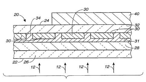
amorphous silicon imaging panel 20. As shown in Fig. 2,
the panel 20 is of a multi-layered structure having an
energy-incident surface 22, through which the
image-carrying x-rays 12 are received, and a
light-detecting surface 24 opposite thereto. Since
aforementioned U.S. Patent 4,672,454, describes a detector
panel of this type in detail, Fig. 2 is intended to~ show
the structure of the panel 20 only schematically as
comprising a light-blocking layer 26, an x-ray
scintillator layer 28 and a two-dimensional array of
photosensitive elements 30 on a glass substrate 32,
numeral 31 indicating an insulating layer filling the
space in between. The light-blocking layer 26 is opaque
to visible light but transmissive to x-rays and may
comprise a thin layer of aluminum. The x-ray
CA 02232381 2000-08-21
- 4a -
scintillating layer 28, which is continuous over the
light-blocking layer 26, is of a phosphorescent material
such as doped cesium iodide or gadolinium oxysulfide
adapted to phosphoresce, when impinged upon by the x-rays
12, to convert the x-ray energy into light energy in a
different range. The light-sensitive elements 30, which
are themselves opaque, comprise an amorphous semiconductor
alloy, and preferably amorphous silicon, capable of
undergoing a detectable change in electrical
characteristic in response to light received from the
x-ray scintillating layer 28. Although not shown in
Fig. 2 (but illustrated and explained in aforementioned
U.S. Patent 4,672,454), the panel 20 further includes
means for individually detecting the electrical
characteristic of these light-sensitive elements 30 and
outputting signals indicative thereof (as shown
schematically in Fig. 1). The light-sensitive elements 30
can be made to have dimensions of only about 90 microns on
a side and hence are capable of representing an x-ray
image with a high resolution. In order to increase
absorption of light from the x-ray scintillating layer 28,
light-transmissive regions 34 between neighbouring pairs
of the light-sensitive elements 30 are minimized but are
yet adapted to transmit light from the x-ray scintillating
layer 28 therethrough to the light-detecting surface 24.
For the purpose of automatic control of the x-ray
dose from the x-ray generator tube 10, detecting means of
different kinds may be used according to this invention,
depending on the energy range expected and the
transmission of the panel 20 to both x-rays and light.
Fig. 2 shows a simple light detector unit 40, which
may be a silicon photodiode or phototransistor, an
avalanche photodiode, or a miniature photomultiplier,
mounted behind the panel 20 (that is, either on its
light-detecting surface 24 or sufficiently proximally
CA 02232381 2000-08-21
- 4b -
thereto such that the separation therefrom will not
significantly affect the amount of light collected from
the x-ray scintillating layer 28). As described above,
there are light-transmissive regions 34 between mutually
adjacent ones of light-sensitive elements 30 through which
visible light emitted from the x-ray scintillating layer
28 passes to reach the glass substrate 32 and received
therethrough by the light detector unit 40. Because the
total light energy that is transmitted is in exact
proportion to the amount of light energy received and
detected by the light detector unit 40, the
proportionality can be easily calibrated preliminarily and
the x-ray dose from the x-ray generator tube 10 can be
easily determined from the charge read out from the light
detector unit 40.
CA 02232381 1998-03-17
WO 98!03884 1'CT/US97/11497
The type of detector unit to be used will depend on the amount of Light which
passes
through the panel 20, depending on the panel transparency and x-ray dose rate.
At high levels,
a simple photodiode is suitable. At very low dose levels, an avalanche
photodiode or even a
photomultiplier might be needed. Because all of these devices axe small
compared to the sample
5 area typically desired, some sort of shaped light collecting device {"a
large area collector") may
be needed. Examples of such a collecting device include a sheet of acrylic
plastic {or polymethyl
' methacrylate).
Another type of detector unit 42 which may be used and illustrated in Fig. 3
is
characterized as being adapted to detect x-rays rather than visible light,
comprising a scintillator
45 in front of a light detector 46. The x-ray beam 12, incident onto the panel
20, is not totally
absorbed by the x-ray scintillating layer 28 to be converted into light
energy. A certain portion
of the incident x-rays penetrates the panel 20 and reappears on the opposite
side. The scintillator
45 is adapted to capture such left-over x-rays and the light energy thereby
generated is received
by the photosensor 46, which outputs a detection signal (riot shown)
indicative of the energy
detected thereby. A detector unit of this type is Less accurate because it
measures the residual x-
rays, rather than the absorbed x-rays directly, but this type of detector unit
may be necessary
where the transparency of the panel 20 is too low to permit direct detection
of the light or where
the scintillator does not produce sufficient light for proper operation of the
detector. Given the
voltage of the x-ray generator tube 10 and the knowledge of particular
technique being used and
the absorption characteristics of the panel 20, however, it is possible to
obtain some approximate
calibration, relating the detection signal with the x-ray dose. It is also to
be noted that amorphous
silicon panels are much more forgiving of exposure errors than films are.
Because the residual
x-rays passing through the panel 20 are generally still well collimated,
unlike the phosphorescent
light emitted from the x-ray scintillating layer 28, detector units of this
kind for measuring Left-
over x-rays need not be mounted directly on the panel 20, as illustrated in
Fig. 3.
Where the x-ray energy is relatively high (say, over 150kev), it may be
desirable to
remove the Light detector unit 40 from the x-ray beam to avoid long-term
damage to the detector
unit. In such a case, a bundle 48 of elongated non-coherent plastic fiber-
optic material may be
used, as shown in Fig. 4, to transmit the light from its light-receiving
surface to the opposite end
connected to the light detector unit 40. A radiation shield (not shown) may be
provided,
whenever necessary.
Although not separately illustrated, a fiber-optic bundles may be used for
bringing
together samples from remote areas on the Light-detecting surface 24 to a
single light detector
unit, or a fiber-optic bundle may be used in connection with a large area
collector.
CA 02232381 1998-03-17
WO 98/03884 PCT/LTS97/11497
6
In situations where it is desired to monitor multiple portions of the panel
20, say, for
adapting to different anatomical examinations, a plurality of detector units
may be provided,
although not separately illustrated. Each of the plurality of such detector
units may be adapted
(being of the type shown in Fig. 2) to detect light from the x-ray
scintillating layer 28 or (being
S of the type shown in Fig. 3) to detect light from its own scintillator, or
the left-over x-rays which
have penetrated and passed the panel 20. In each of such applications, fiber-
optic bundles may
be used as shown in Fig. 4.
Fig. S shows an example of exposure control means SO for controlling the x-ray
IO generating tube 10 (shown in Fig. 1) according to the outputs from the
light detector units 40 or
42, especially where a plurality of such detector units are used in the
system. Output signals
from the light detector units 40 or 42 are received by a selector switch S2,
of which the function
is to select one of the plurality of detector units in response to selector
control signals S3 inputted
by the user and to allow only the detection signal from the selected detector
unit to pass
1S therethrough. The detection signal which has been allowed to pass through
the selector switch
S2 is amplified by a signal amplifier S4. The amplified detection signal
serves directly as the
instantaneous dose output to control the x-ray dose from the x-ray generator
tube i0 for online
fluoroscopy. A portion of the amplified detection signal may be received by a
signal integrator
S6 to calculate the total dose represented by the received during a specified
time interval between
20 a start time and a stop time inputted through a start/stop control signal
S7. The output from the
signal integrator S6 serves as the total dose output to control the x-ray
generator tube 10 for
single-shot fluorography.
Such a control system with a switch suffices where only simple examinations
are to be
2S performed. Since each detector unit may include sampling of an extended
area by use of light
collectors and since there may be overlapping areas, a one-to-one anatomical
programming
method is possible. This scheme requires much advance planning, however, so a
more complex
method and scheme may be desirable.
30 Fig. 6 shows another example of exposure control means 60 which allows
proportional
mixing of the various signals as required by the anatomical configurations.
Detection signals
from the plurality of detector units are individually amplified by
corresponding ones of signal
amplifiers 61 and received by a weighting means 62 for proportionally mixing
these individually
amplified detection signals according to the weighting scheme communicated
through weighting
3S control signals 63 inputted by the user. In other regards, the control
means 60 of Fig. 6 is the
same as shown in Fig. S and hence these components that may be identical are
indicated by the
same numerals and not repetitively described.
CA 02232381 1998-03-17
WO 98/03884 PCT/US97/11497
7
With exposure control means as shown in Fig. 6, substantial additional
flexibility can be
provided in the control. An additional switch (not shown) may be provided to
permit remote
selection of the proportional or integrated signal outputs rather providing
these on separate lines.
The invention has been described above with reference to only a limited number
of
examples, but these examples are intended to be merely illustrative, not as
limiting. Many
modifications and variations are possible within the scope of this invention.
For example, the
direct light detection schemes of this invention can be applied also to any
light-detection
applications for panels, not limited to those in which Iight is generated by
an x-ray scintillator.
In fact, any spatially distributed image-carrying form of electromagnetic or
accelerated particle
(such as electron) beam energy within an appropriate energy range can be used
on an appropriate
(such as solid state) energy converting means to generate light in another
energy range. This
invention has applications to a variety of scientific instruments in which
optimum performance
depends on reception of a su~cient amount of accumulated light before read-
out. In summary,
all such modifications and variations that may be apparent to a person skilled
in the art are
intended to be within the scope of this invention.