Note: Descriptions are shown in the official language in which they were submitted.
CA 02232472 1998-03-17
~ t
~ _ WO 97/12458 PCT~E96/01212
CLOCK SELECTOR SYSTEM
TECHNICAL FIELD
The present invention relates to distribution of a clock signal comprising reclunrl~ncy to a
user of the signal and in particular how a clock signal is sele~tP~1 among several available
5 clock signals.
BACKGROUND AND STATE OF THE ART
In the field of telephone connections and in telecommunication equipment generally, as a
rule there exists a need for distribution of two clocking signals, herein called clock and
synchronizing pulse rates, the latter one called " synch rate" in short, to various sub-
oequipments and components therein. This distribution is particularly wide in physically largeconnP~I~l systems, such as in the type of switches having various multiplexing stages and
similar units. The clock rate has generally a high frequency and among other things defines
borders for bits in the data flowing through the equipment and the synch rate has a low
frequency and defines frame borders and similar things in the data signal. The number of
signals transferring clock and synch information in an equipment such as a
telecommunication switch station can be rather large and in the following the general
"e.~ion "the clock distribution network" is used therefor. Telecommunication equipment
in a m~g~7ine or cabinet, etc., has a considerable multitude of tr~ncmiccion components for
rate distribution in the shape of cables, pins in back planes and electrical terminals, lines in
20 back planes, etc. The space required for all such signal connections is considerable and costs
money. As a rule, the number of pins in a connector is a small resource limiting the size of
for example a switch.
In equipments having large requirements of their reliability the clock distribution
network must of course also fulfil large reliability requirem~ntc The reliability of the clock
25 distribution network can be enhanced, in the conventional way, by introducing redl-n~ncy.
If the clock distribution and the clock source are designed to include redundancy, i.e. that
they may be duplicated or, as is supposed in the following herein, in the ~lt;r~ d case
triplicated, a redlln{l~nt and triplicated clocking structure can be m~int~ined from clocking
source to clocking receiver, however, in the receiver end one of the clocks must of course be
30 sel~tt--d for operational use by the respective equipment.
In previous systems not having redundancy, where clock rate and synch rate are to be
distributed to all m~g~7:ineS and cabinets, as a rule two coaxial cable have been used to each
receiver or user of the rates, one coaxial cable for the high frequent clock rate and one cable
for the low frequency reference rate, that we call also the frame rate or the synch rate
35 herein.
For distribution of clocking rates, where the high frequency clock is distributed
separated from the low frequency synch rate, the precision must be great so that for example
the pulses in the synch rate will not end up or be interpreted at the wrong one of the edges
of the clock rate pulses. This poses among other things great requirements on the similarity
~o of the lengths of the two cables used for clock and synch rate, respectively, in relation to
each other and also in relation to other pairs of cables having other clestin~tions in the
CA 02232472 1998-03-17
- W O 97/12458 PCT/SE96/01212
system.
Distribution of a clock signal which has a very high frequency and by means of which
circuits in telecommunication systems presently generally operate, in addition poses large
requirements on the ~hiel~iing of cables and connectors, etc. together with good grounding
5 conne~tion~ and similar things, so that interference protection and functionality can be
provided and also maintained during a long time.
In for example large switches having circuits on circuit boards in m~g~7ines and cabinets
there is thus a need for distributing a clock having a relatively high frequency and a rate
having a lower frequency as a reference for frame structures, etc. Clock rate and synch rate
lO can be distributed in the shape of a single, composite signal ("Composite Clock Signal"),
herein called CLSY (CLock and SYnch), as described in the International Patent Application
PCT/SE94/00321, which is incorporated herein by reference.
This signal comprises a clock frequency or clocl~ rate that has a frequency considerably
lower than the real system frequency at which the circuits of the system operate, i.e. is
5 advantageously an even fraction thereof such as 1/36 thereof, and it further comprises a
synch frequency or synch rate that is modulated on top of this clock frequency and
advantageously is an even fraction, such as 1/640, thereof.
A phase-locked loop circuit, PLL, is provided with logic circuits inL~ tillg the synch
information in the composite CLSY signal and it also generates a clock signal having a
20 frequency that is considerably higher than the clock frequency of the CLSY signal, such as
for example in a similar way as above, 36 times thereof. The PLL issues the synch pulse
with a precision in relation to the system clock that would have been very difficult to
produce using conventional clock distribution on two separate lines.
The advantages of distributing a frequency in the shape of CLSY, that has a considerably
25 lower frequency compared to the system clock and in addition is provided with synch
information and of arranging for a PLL to generate the system clock rate together with synch
rate are:
1. The signal can be distributed more easily from an EMC point of view, i.e. in regard
of sensitivity to interference from the outside and in regard of its own interfering inflllen~e
30 The distribution medium must not have the same precision as in the case where system clock
and synch rate would have been distributed separately. This implies that for in~t~nçe a single
optocable can be used.
2. Pins and space in connectors and back planes, etc. are saved by using the same
physical signal paths for both clock rate and synch rate.
3. A very good precision can be achieved by the arrangement that the PLL generates
both the system clock and the synch on the same chip and from the same signal.
Redundant clock distribution systems are disclosed in the documents discussed briefly
hereinafter and also in other documents.
In the Japanese Patent Application JP-A 60-225982 clock pulse synchronization is40 described in a triplicated system. A harmful influence of errors is prevented by correction by
means of majority decisions.
CA 02232472 1998-03-17
- WO 97/12458 PCT~E96/01212
In U.S. Patent US-A 4,185,245 an arrangement is described for fault-tolerant clock
signal distribution. First and second redundant clock signal sources are arranged. Clock
receivers include sequential logic circuits for examining the two clock signals in order to
ignore the clock signal pulse train that comes after the other one as to the phases thereof.
U.S. Patent US-A 4,489,412 discloses a network comprising supply of clock and
synchronizing signals by means of clock distribution modules that perform majority voting
for output signals from three oscillators.
U.S. Patent US-A 4,692,932 is related to triplicated clock distribution, each clock signal
including a synchronizing signal. In the receivers R logic circuits for majority voting are
oinrl~lded comprising three AND-gates and one NOR-gate in each receiver. These majority
circuits pass only the input clock signal that has a phase position located between those of the
other two clock signals. No tests are made of the quality of the received clock signals in the
receivers in order to make the selection.
In U.S. Patent US-A 4,698,826 triplicated clock distribution is described. Each clock
outputs a signal including a clock signal and a synchronizing signal.
U.S. Patent US-A 5,065,454 discloses a clock signal distribution arrangement having
redund~nt clock generation. The distribution paths are duplicated for redundancy reasons.
The European Patent Application EP-A2 0 365 819 treats the problem of synchronizing
the individual clocks in a multiprocessor system. A number of clock sources have each one
20its PLL circuit, see column 10, lines 31 - 58. The clocks transmit reference signals to each
other which are subjected to a selection operation in each clock.
The European Patent Application EP-A2 0 366 326 treats the problem of ensuring, in a
computer system in which a number of clock signals are derived from a main oscill~tnr
signal, that the clock signals appear at the right times where they are needed It requires the
25 introduction of a small time delay between the clock signals in order to compensate for
differently long transmission paths. The solution described aims at reducing the risk of errors
in the time delays of the different clock signals. A PLL circuit is used for m~int,.ining a
phase relationship between each clock signal and a reference clock signal.
In U.S. Patent Document US-A 4,239,982 a fault-tolerant clock system is disclosed that
3C is intended to produce system clock signals by means of several clock sources. Each clock
source receives as input signals the clock signals generated from all other clock sources and
cont~inc receiver circuits for deriving a system clock signal from these clock sources. Each
clock source generates and distributes to the other clock sources a clock signal that is locked
in phase to the system clock derived from its clock receiver. The system allows the use of
35 high clock frequencies comprising a minimum phase jitter between derived system clock
signals.
In the European Patent Application EP-A2 0 303 916 four rate signals that are
synchronous as to frequency and phase are generated, for providing timing for e.g. a
computer system. The generation of the rate signals is made by means of four PLLs, the
40 output signals of which are fed to four selector circuits, in which a type of majority voting is
performed. The signal selected by a selector circuit is fed back to a definite one of the rate
CA 02232472 1998-03-17
_ W O 97/12458 PCT~E96/01212
generators for controlling it. Delay circuits are introduced for adapting the phase position of
the selec~Pcl signals. Such delays cannot easily be introduced in the case where the clock
signal contains both a clock and a synchronizing rate, the latter one having a low frequency.
In U.S. Patent US-A 4,105,900 a triplicated control system is disclosed in which three
5 redundant sensor signals are used, one of these signals providing precise information and the
rem~ining two ones less precise information. A selection of signal according to a pre-
programmed priority order is based on the operative state of the three sensors.
SUMMARY
It is an object of the invention to provide a redllnd~nt clock signal distribution system
10 that when the system is regarded reduces "phase jumps" of the clock signal.
It is a further object of the invention to provide a redundant clock signal distribution
system that is suited for connecting clock signals in cascade between different stations.
In an electronic system for transferring and processing information, clock signals are
distributed that can be generated centrally to different subsystems. The clock signal
5 distribution is made redundant by distributing several clock signals that are identical in
principle, which when they are generated are identical at least in regard of the timing
information contained in the clock signals. In a first station is select~od, by means of a clock
selector circuit, one of the received clock signals as that clock signal which is to be used in
the station. Then the first station is made to switch the selected clock signal among the
20 different clock signals periodically according to some scheme. In this way a time average is
formed of the phase positions of the arriving clock signals, what reduces the "phase jump"
that can arise in the case where some of the arriving clock signals becomes faulty and does
not exist any longer among those clock signals which are repeatedly and cyclically se]e~tecl.
The timing information is retrieved in the first station from the selected clock signal by
25 means of a phase-locked loop circuit, PLL. The selection of a new clock signal can be
performed with a frequency that is much higher than the limit frequency of the phase-locked
loop circuit, so that jitter caused by the clock selector alternating between clock signals that
present phase differences in relation to each other is reduced.
For achieving a local clock signal distribution one can let the selected clock signal also
30 be a clock signal for other stations located nearby, i.e. the clock signal can be connected
succecsively through several stations connected in c~c~-le Further, the clock selector
circuits in the first station can also be made with redundancy, so that independent selections
of a clock signal are made in several different planes in the first station. When these
selections are made so that they are cyclically repeated between the arriving clock signals
35 according to the above, all redundant planes will select clock signals that have the same
average, in particular in regard of their phase positions. Hereby phase errors between the
clock signals used in a plane in a first station will be reduced significantly when the clock
signals are communicated to a cascaded station.
Redundancy of an electronic system, for instance an information processing system or a
40 telecommunication switch, inclusive of the required clock functions can be produced by
triplicating all hardware for enhancing the reliability, i.e. several identical units called planes
-
CA 02232472 1998-03-17
W O 97/12458 PCT~E96/01212
s
are made to each one alone and independently perform the required functions and execute the
required processes in parallel. Majority votes can be used for excluding a faulty plane.
Generally thus, a clock signal is distributed in an electronic system such as some type of
network or electronic in~t~ tion~ for example for procescing information, for exe~lting
5 processes in different stations or for forwarding information between stations, the clock
signal being used for control. At least two different clock sources are arranged for gent~rating
clock signals that contain substantially the same timing information. To a first subsystem the
clock signals are transferred on individual lines or on different independent comm-lnic~tion
channels from each clock source to the first subsystem for supplying the clock signals as
10 clock signals arriving to the subsystem. Selector means in the first subsystem pe,ro~ a
selection of a clock signal among the received clock signals.
By means of particular means or devices that include the selector means in the first sub-
system it is achieved that that clock signal which is selected by the selector means in the first
subsystem is constantly exchanged for a new selected clock signal. This presupposes
15 naturally that there are at least two received clock signals among which to select, what
perhaps is not always the case, see below. In the first subsystem then a time average is
obtained of the phase positions of the clock signals, as regarded over a time period
comprising several changes of clock signal. The changes to a new selectPd clock signal in the
first subsystem can be made cyclically and/or in a way regular in time. In the latter case it is
zo meant that if for instance three signals A, B, C are available a change from A to B is made
after a first predetermined time period, a change from B to C after a second predetermined
time period and a change from C to A after a third predetermined time period.
Similar to the construction disclosed in the International Patent Application cited above a
phase-locked loop can be provided to which a line is arranged from the selector means. The
25 phase-locked loop receives on this line the clock signal selected at each time instant and is
arranged to produce therefrom a second clock signal, which for example can be used for
controlling processes in a subplane in the subsystem. The means for changing to a new
sel~cted clock signal can then advantageously be arranged to perform the changes so often
and the phase-locked loop can be so arranged, that the phase position of the second clock
30 signal will be subst~nti~lly free from jitter. This can be achieved by the fact that the phase-
locked loop has such a time constant, that it, at a change to a new selected clock signal, only
to a limited degree will have time to adapt to the phase position of the new clock signal. A
phase jump can obviously be obtained at a change to a new clock signal and then the phase-
locked loop will start to somewhat change the phase of the provided second signal, but a new
35 selection and a new phase jump will occur before the phase has changed very much.
Comparison and evaluation means can be provided in the first subsystem for co.-l~a ing
and evaluating the received clock signals for determining those clock signals that are correct
and in that case the selector means are advantageously connected to these comparison and
evaluation means for performing a selection of a new clock signal only among those clock
40 signals which have been found to be correct by the comparison and evaluation means.
For the constant change of clock signal in the first subsystem the means arranged
,
CA 02232472 1998-03-17
- WO 97/12458 PCT~E96/01212
therefor can include the clock sources and they are then arranged to provide all clock signals
with artificial errors and to introduce the errors so that they are dete~ted by the co~ a ison
and ev~ tion means in the first subsystem. Hereby the selector means in the first sub-
system, when dPtecting errors, will select a new clock signal and in this way the permanent
5 changes of clock signal can be achieved.
The comparison and evaluation means in the first subsystem can, for achieving
re~und~ncy, include at least two units working independently and in parallel and in particular
an equal number of units working independently and in parallel as there are clock signals
arriving to the first subsystem.
10 In an analogous way at least two selector units that work independently can be
incorporated in the selector means in the first subsystem and in that case lines are arranged
in the first subsystem for communicating the signals on all the independent lines or ch~nn~
connected to each of these selector units. Each selector unit is then arranged to perform,
independently of and in parallel to the other selector unit or selector units, a selection of a
5 clock signal among the arriving signals for producing several selected clock signals obtained
in parallel.
Also the selector means in the first subsystem can advantageously comprise an equal
number of selector units working independently and in parallel as there are arriving clock
signals to the first subsystem.
Further, the first subsystem can be connected in c~ca(1e to a second subsystem, which
then is to include selector means in substantially the same way as the first subsystem. On
individual lines or different, independent tr~n~miss-on ch~nnel~ from each selector unit
included in the selector means in the first subsystem these at least two clock signals se1e~teA
independently in parallel by selector units are supplied as clock signals which arrive to the
25 second subsystem or possibly are included among the clock signals which arrive to the
second subsystem.
BRIEF DESCRIPTION OF THE DRAWINGS
The invention will now be described as a non-limiting exemplary embodiment with
reference to the accompanying drawings in which
- Fig. I is a block diagram of a clock distribution system,
- Fig. 2 is a diagram illustrating the structure of a frame in a clock signal,
- Fig. 3 are wave form diagrams as functions of time that illustrate various subsequences
of the clock signal frame,
- Fig. 4 is a block diagram of a clock selector unit,
3~ - Fig. Sa is a block diagram of a frequency error detector,
- Fig. 5b is a wave form diagram of a section of a composite clock signal containing a
synch sequence,
- Figs. 5c - Se are wave form diagrams of output signals from various circuits
illustrating how an isolation of a synch pulse is made,
- Fig. 6a is a block diagram of a phase error detector,
- Fig. 6b is a block diagram of a differentiation circuit used in the phase error detector,
CA 02232472 1998-03-17
_ W O 97/12458 PCT~E96/01212
- Figs. 6c - 6e are wave form diagrams illustrating the signal proce~cing in thedifferentiation circuit,
- Fig. 6f is a block diagram of a coincidence detector used in the phase error detector,
- Figs. 6g - i are wave form diagrams illustrating the signal proc~ccing in the
5 coincidence detector,
- Fig. 6j is a block diagram of a time interval monitoring unit used in the phase error
detector,
- Fig. 6k is a state diagram of a hysteresis circuit used in the phase error detector,
- Fig. 61 is a time diagram illustrating the states of the hysteresis circuit,
o - Fig. 6m is a block diagram illustrating how phase errors are monitored,
- Figs. 6n and 6O are wave form diagrams illustrating the function of a hold circuit,
- Fig. 7a is a block diagram of a clock selector control,
- Fig. 7b is a truth table of a combinatorial circuit used in the clock selector control,
- Fig. 7c is a state diagram of a state machine used in the clock selector control,
15 - Fig. 8 is a schematic block diagram of a unit for selecting a clock signal and for
producing a system clock and a synch rate.
DETAILED DESCRIPTION
The following detailed description is based on a clocking signal called CLSY (CLock
and SYnch signal), see the discussion above and the International Patent Application
20 PCT/SE94/0032 1 mentioned above.
The CLSY signal is a composite clock signal that is composed of a clock signal "clock"
which hereinafter is ~cumed to be chosen to 5.12 MHz and is a pulse signal, typically a
square wave signal, having a frequency that is here called the base frequency or the base
band frequency, and a synchronizing signal "synch" having a frequency that hereinafter is
2s~csllme~ to be chosen to 8 kHz. The clock frequency that is supposed to be used in the
system of the different "useful components" thereof is 184.32 MHz and is also called the
frequency of the system bit clock or the frequency of the system clock, but in order to be
able to distribute more easily clock rates in the system the clock rate is distributed in this
way having a lower frequency, the base band frequency in order to be, on the receiver side,
30 i.e. in each unit that needs a system rate, multiplied by a factor of 36 in a PLL, a phase-
locked loop circuit, in order to obtain the desired system clock of 184.32 MHz. The PLL
also decodes the synchronizing signal that is included in the CLSY signal. The PLL has also
the quality of being insensitive to the cases where single pulses in the input signal are
omitted or where there are single spikes in the input signal.
35 Inside the CLSY signals codes for maintenance testing are also provided. These codes or
patterns supply information in regard of the plane in which a considered CLSY signal is
generated and further, they emulate certain errors for maintenance testing the hardware.
There are several advantages of the CLS Y signal, as has been indicated above: phase
differences between clock rate and synch rate are reduced, the number of physical signal
40 conductors is reduced and ~phase jumps" will have magnitudes of at most 1/4 of the period
of the synch and clock rate respectively, i.e. of the periods corresponding to the frequencies
CA 02232472 1998-03-17
.,
- WO 97/12458 PCT/SE96/01212
of 8 kHz and 5.12 MHz respectively.
The logical architecture of the generation, distribution and termination of the clock and
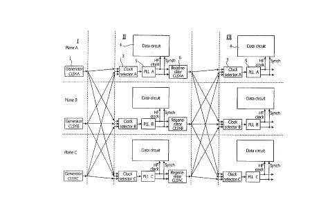
synch signal will first be described at a general level. ln Fig. 1 it is shown in principle, how
three generators 1 create the composite clock signals, the CLSY signals, i.e. three equivalent
5 composite signals here called CLSY-A, CLSY-B, CLSY-C, that contain both a clock rate
and a synch rate. These composite clock signals are distributed from each generator 1 to
each one of three clock selectors 3 that terminate the triplicated distribution. ~n each such
clock selector 3 an independent choice is made, independent of the other two clock selectors,
of the "best" clock signal by evaluating the different received clock signals and comparisons
10 thereof. Thereafter the selected CLSY signal passes from each clock selector 3 to a following
phase-locked loop circuit 5, PLL, in order to be separated there in its components, the clock
rate and the synch rate, respectively, and for generating a system bit clock. The system bit
clock and the synch rate are used in each plane by various electronic circuits that are
schern~tic~lly illustrated by the triplicated data circuit 4 in Fig. 1.
Each one of the oscillators 1 is constructed so that it creates a composite clock signal, a
CLSY signal, containing pulses or pulse patterns for definition of clock rate and synch rate
and further also sequences of pulses or changed or modified pulses that imitate errors, for
m~inten~nce testing following clock selectors 3, and also, hidden in the pattern of pulses for
clock rate and synch rate, by the method that some pulses have been changed, an identity
20 code comprising information on the plane in which the considered CLSY signal has been
generated, i.e. whether it has been generated by the oscillator in plane A, B or C. "Artificial
errors" in the CLSY signal are created by the method that a CLSY generator 1 introduces the
errors in the composite clock signal already from the beginning, so that the errors constitute
a natural part of the CLSY signal. By this method it will not be possible to remove or add
25 artificial errors on command.
The task for a clock selector 3 is to autonomously select a working composite clock
signal among the three arriving clock signals CLSY-A, CLSY-B, CLSY-C. Criteria of the
fact that a CLSY signal is to be considered as correct is that its frequency is correct and that
its phase position in relation to the two other CLSY signals is to be located within certain
30 limits. The clock selector 3 thus makes an autonomous judgement of the frequency and the
phase position in relation to each other of the arriving clock signals and selects according to
an algorithm one of the input signals, which is communicated to the output terminal of the
clock selector 3 through a multiplexer in the clock selector 3. The clock selector is thus
m~i"ten~nce tested by means of artificial errors which are always included in the CLSY
35 signals. Further, the artificial errors are entered so that the clock selector 3 will run through
all accepted clock signals and in particular so that it periodically and in a pattern that is
regular in time changes cyclically between them. In this way it is constantly verified that it is
possible for a clock selector 3 to actually select anyone of all accepted composite clock
signals. By using this method no signals are to be provided that are outside the functional
40 clock distribution, but the signals needed for the maintenance testing are always incorporated
as a part of the functional clock signal.
CA 02232472 1998-03-17
_ W O 97/124S8 PCT/SE96/01212
, .
The funetion of a PLL S is, às has been mentioned above, to separate the arriving CLSY
signal in its eomponents, signals for eloek and synch rate respectively, to multiply the
extraeted eloek frequeney to the system bit frequeney of 184.32 MHz, to filter out ID-eodes
and ernul~t~i, i.e. intentionally introdueed, error patterns, to eonvert abrupt phase jumps to
5 slow phase drifts and to filter jitter that ean exist in the input signal to the PLL 5.
In order to obtain a high MTBSF (Mean Time Between System Failure) for the eireuits
and eonnections in the system, it is important that as many as possible of the possible errors
that ean arise in the hardware ean be safely deteeted. It is also important that a possibility
exists of loealizing an error as well as it is important that no errors are prop~g~t~ through
10 the system and thereby give the system worse eharaeteristics.
In order to obtain this, it is naturally important that the maintenanee funetions are as
reliable as possible. Further, if a hardware error would appear in the very ~ t~ nce
funetions, this should also be possible to detect wherever the error has arisen. Similarly, the
design of the system should not be such that an error actually has arisen in some part that
15 influences the main task of the system and that the maintenance functions are not eapable of
cleteeting this error owing to some error in the maintenance funetions or some other error or
owing to an imperfeet construction.
To use a single static hardware signal, that informs on alarm state, thus "OK" or "not
OK", must be eonsidered as unreliable, as has been mentioned above. A hardware error ean
20 have arisen in the hardware communicating the signal, so that the information of the signal is
erroneous. It can indicate "error" even if it is "OK", or indicate "OK" in spite of being
"error" .
In the design of maintenance systems for clock functions the prineiple is used that at
least two different signals in the hardware are to be supervised by software and the eriterion
25 of the fact that the system is to be judged correct should be that there must exist a eertain
relation between these hardware signals and further, that the hardware signals should not be
statie, but that they instead should be con~tituted by either eounters or flags, whieh ehange
aeeording to a predetermined pattern, for example such as that a certain flag is set at some
oceasion and then is reset at another oceasion. The software should then require that the
30 expeeted dyn~mies7 i.e. the serial order in whieh the flag is set and reset respeetively, exists
all the time and that otherwise an alarm signal is generated in the software.
The funetion of a eloek seleetor 3 is aeeording to the diseussion above mainly both to
select away, at eaeh time instance, a badly working clock and to select among the rem~ining
eorreet eloek signals a working clock signal CLSY-A, CLSY-B or CLSY-C. In order to
35 check whether a elock seleetor 3 is working, that elock signal which at a considered time
instant is seleeted by the considered clock selector 3, is deteriorated by the perm~nently and
intentionally introduced errors, and supervising functions check that the clock selector 3 then
is eapable of selecting another composite clock signal.
The clock signals, the CLSY signals, are therefor, as has been indicated above, made to
40 contain, already from the start, pulse sequences which imitate defective clock signals. The
CLSY signals are generated in the construction blocks that are called CLSY generators 1 in
CA 02232472 1998-03-17
_ WO 97/124~8 PCT/SE96/01212
Fig. l. The artificial errors which are found in a CLSY signal are further entered so that
they correspond to criteria that define the clock qualities which the clock selector is to accept
or not accept, respectively.
From a clock selector 3 the selected CLSY signal is provided and in order to be able to
5 decide if it is that CLSY signal that the system should select or think that it has .';ele~t~d, the
CLSY signals have, according to the discussion above, also been provided with identity
codes, ID-codes, during the generation of the signal. The CLSY signal that is generated in
the A plane, is thus called CLSY-A and is provided with an identity code A, in~ in~ that
the CLSY signal has its origin in the A plane. In the corresponding way the CLSY signal
10 from the B plane is provided with an ID-B code and the CLSY signal from the C plane with
a code for C. By monitoring the CLSY signal provided from a clock selector 3 superior
functions in the system can determine the identity of the CLSY signal that has been se1ect~
A CLSY signal is divided into frames which each one has a length of 125 microseconds,
i.e. the frames are repeated with the frequency 8 I~Hz which is the same as the synch rate,
sand they comprise 640 cycles or periods of the clock rate signal of 5.12 MHz. Further each
pulse or period of the clock rate signal can be considered as two halfperiods, where a
transition, positive or negative, can occur, and using this way of looking then 1280 data bits
exist in each CLSY frame. These bits are numbered from l up to 1280 as is shown in Fig.
2. A CLSY frame is divided into 8 subframes and each subframe is divided into three sub-
20 sections, the first and second subsections of which each one has a length of 54 bits and thethird subsection of which has a length of 5 bits.
In the beginning of each CLSY frame a pattern is provided for frame recognition and
this pattern is called a synchronization pattern or synchronization sequence that indicates a
synch pulse. It is this pattern that a PLL 5 recognizes and each time that this pattern is
25 recognized by a PLL 5, the PLL 5 generates a corresponding synchronization pulse. This
synchronization pattern increments, for each time that it appears on the output of the
multiplexer of the clock selector, a counter for synchronization patterns as will be described
hereinafter.
In each CLSY frame two ID-codes are arranged, naturally denoting the same plane. In
30 the CLSY signal generated in the A plane two ID-codes for A are provided. Thecorresponding condition applies to CLSY signals generated in the B and C planes.In Fig. 3 subsequences of the CLSY frame that are schematically illustrated in Fig. 2 are
shown as wave form diagrams. The numbers within squares in these figures col~sl~olld to
each other. In the CLSY signals particular bit sequences or pulse sections of the pulses in the
35 base band frequency are arranged that indicate synchronization pulses S for each frame,
frequency reiect sequences F, phase reject frequencies P and identity codes ID-A, ID-B, ID-
C. Each frame thus starts with a synchronization sequence S. Within each subsection of a
frame there is an intentionally introduced error sequence F or P for simulating frequency
errors and phase errors respectively in a single one of the three clock signals. The ~ t~nt~e
40 from a frequency reject sequence F to the following border between two subsections in the
frame is always constant. The distance from a phase reject sequence to the most nearly
CA 02232472 1998-03-17
_ W O 97/12458 PCT/SE96/01212
11
located, following border between subsections is also constant but has a value which is
dirre-e.-t from the ~list~nce that applies to the frequency reject sequences and which in
particular is less than it. The ID-codes ID-A, ID-B, ID-C always follow directly after a
border between two subsections, i.e. they arrive first or early in a subsection, before the
5 error sequence therein. The error sequences F or P always follow in the later part of a sub-
section, so that in a subsection there is room for both an identity code and an int~ntion~ly
entered error sequence.
The frequency reject sequences F consist of the device that two pulses in the base
frequency have been omitted and that during them a smooth low voltage level exists and in
10 the same way the phase reject sequences P consist of the device that three pulses in the base
band frequency have been omitted, i.e. they are one pulse longer. The phase reject sequences
P occur in each clock rate frame only once in each clock signal, i.e. in only one subsection.
In other subsections there is a frequency reject sequence F in only one of the composite
clock sign~l~ Identity code sequences ID-A, ID-B, ID-C occur twice in each frame and each
15 individual clock signal. They consist of the device that two pulses are omitted having a
different number of remaining pulses therebetween, in particular one, two or three rem~ining
pulses for the identity code sequences ID-A, ID-B and ID-C ~ ,ec~ively.
Using the preferred arrangement, which will be described in greater detail hereinafter, a
clock signal selector 3 that works correctly will select CLSY-A as an output signal during the
20 first subsection in each subframe, it will select CLSY-B during the second subsection in each
subframe and CLSY-C during the third subsection in each subframe. A new selection of
clock signal will then thus be perfonned at each vertical, thin or thick, line in Fig. 2. There
will always be time to perform this, before the next intentionally entered error sequence is
d~ct~i and also before encountering an ID-code.
A clock selector 3 comprises, as has been mentioned above, a multiplexer and it has
three input terminals and one output terminal and one address input terminal controlling the
multiplexer, see the detailed description hereinafter. The control address is generated
autonomously in control logic circuits in the clock selector that sense quality, phase position
and frequency of the three arriving CLSY signals and from these measurements and certain
30 other criteria, as given by an internal state machine, determine the clock that is to be selected
and is to be provided from the selector. On the output side of the multiplexer a device is
provided recording ID-codes. Alternatively the ID-code of the selected composite clock
signal can be obtained directly from the control logic circuits. For each ID-code A that is
detected on the output terminal of the multiplexer, a counter for ID-A pulses is incremented.
35 The corresponding counters are provided for ID-B and ID-C. In addition to counters for ID-
codes also, as has been mentioned above, a counter is provided for the number of detf~rt~fl
synch patterns, where each synch pattern defines a clocking pulse for the synchronization
rate.
Also on the input side of the multiplexer an arrangement is provided comprising ID-code
40 counters that will be described hereinafter. On the input of the multiplexer where the clock
signal CLSY-A from the generator A is expected to arrive, a device is provided sensing ID-
CA 02232472 1998-03-17
_ W O 97/12458 PCT/SE96/01212
12
A pulses and for each pulse a counter is stepped. At the input terminals of the other clock
signals CLSY-B and CLSY-C of the clock selector or multiplexer corresponding counters for
ID-B pulses and ID-C pulses are provided.
The principle of verifying that the clock selector works is that the software reads the
5 number of counted ID-codes and checks that the counted numbers of ID-pulses A, B and C
on the input side of the multiplexer agree with the number of counted ID-pulses and synch
pulses on the output side of the multiplexer. In order that the counted pulses are to
correspond to one and the same period, all counters are reset simultaneously at a certain time
and before the count values are read, the incrementing thereof is simultaneously stopped.
o Software is arranged taking care of the m~inten~nce functions. This software reads at
certain intervals the counter values. After all counters have been read, they are reset and
before they are read, their counter values are frozen simultaneously according to the
discussion above so that they are not updated any further. Thereby all counter values will
correspond to one and the same time period.
In order to explain the number of counted pulses or, more exactly, the relation which is
to exist between different counter values that have been recorded by the counters in a clock
selector 3, for a correct function, it will first be described in greater detail the way in which
the CLSY signals are constructed. It should be observed that the PLL 5 that is provided after
a clock selector 3 is insensitive to both ID-codes and artificial error sequences, emulated
20 errors, by the fact that it can only change relatively slowly. It can also be observed, that the
triplicated distribution of clock signals in to a clock selector after the clock selector is no
longer triplicated. Neither is the PLL 5 triplicated in the respective plane, but in contrast
there is a PLL 5 in each plane, so in this way also the PLL is triplicated. If any of the PLLs
breaks down, it is observed by the fact that the whole plane goes faulty. It is not n~cRs~ry to
25 supply maintenance checks of a PLL 5, since an error in a PLL 5 is visible. In the system
erroneous PLLs ~ cannot exist without being observed. An error in a clock selector 3 would
in contrast exist if special m~inten~nce functions for the detection thereof were not provided.
For ~y~mple it could be so that the clock selectors in the A plane and the B plane owing to
some fault cannot select any other clock than for example A. The system will then work well
30 as long as the clock A exists and is correct, although the redundancy does not work in the
intended way. Then it is enough that an error arises in the CLSY generator 1 in the A plane
in order that the whole system will stop to work. It is thus important to provide reliable
maintenance functions in the clock selector 3 in order to ensure that no errors exist there.
The CLSY signals and the functions in the clock selector 3 are adapted to each other in
35 order that cycling between clock signals and maintenance testing will be provided. In
particular the clock selectors 3 are designed for excluding signals having phase errors and/or
frequency errors. Knowing how the detectors for the phase and/or frequency errors are
made, particular patterns can be entered in the CLSY signal which make that the detectors in
the clock selector for phase and frequency errors, respectively, are used all the time.
The phase monitoring is made in the following way: The phase position between each
pair of CLSY signals, i.e. between A and B, between B and C and between C and A, is
,
CA 02232472 1998-03-17
- WO 97/12458 PCT/SE96/01212
13
che~k~d by the method that the edges are not allowed to be separated in phase (= "skewed")
by more than a certain number of nanoseconds, "the phase acceptance window", which for
example can be set to about 44 to 49 nanoseconds, what will be discussed in greater detail
hereinafter. The positive edges in each CLSY signal are converted to a pulse having a
s definite duration that is equal to the width of the phase acceptance window. These pulses are
called differentiation pulses. The differentiation pulses from the two planes that are to be
compared in regard of phase, are connected to an AND-gate. If the two CLSY signals are
separated in phase by more than the width of the differentiation pulses, there will be no
logical one as output signal from the AND-gate. However, if the signals are in phase or are
lO not s~aldted by more than the width of the phase acceptance window, a logically true signal
will be generated as output signal from the AND-gate, since both of the differentiation pulses
are logically true during a time period. The signal generated in that way as output signal
from the AND-gate is called a coincidence pulse. Knowing that in a normally working
system the CLSY signals are not separated as to their phases by more than the width of the
sphase acceptance window, i.e. that all differentiation pulses will result in a corresponding
coincidence pulse, and the differentiation pulses, that are generated from the positive edges
in the respective CLSY signal, have a periodicity of at most about 600 nanoseconds, the
result will be that the time period between coincidence pulses will agree with the time period
between simultaneous positive transitions or transitions, i.e. at the longest about 600
2O7~l~noseconds. The time period between the coincidence pulses is monitored and constitutes a
measure whether the two CLSY signals are in phase with each other: In the case where the
time period is below 650 nanoseconds, the signals are said to be in phase with each other. In
the case where the time period is above 650 nanoseconds, at least two differentiation pulses
have not arrived sufficiently simultaneously (not with a sufficient overlap), are thus separated
25 by more than the width of the phase acceptance window and are thus not in phase with each
other.
In order to verify whether the phase supervision works, a suitable number of positive
transitions in the CLSY signal can be removed. Then will, in the case where the phase
monitoring logical circuits work, a corresponding phase alarm be generated and a change of
30 clock is made in the clock selector 3.
If a phase error exists, a real or "genuine" one or one produced by manipulating the
CLSY signal, for example in CLSY-A, the phase monitoring logic circuits will observe a
phase error of the clock signal A and the clock signal B in relation to each other and of the
clock signals C and A in relation to each, but not of the clock signals B and C in relation to
35 each other. By means of decoding the information from the phase monitoring logical circuits
in a combinatorial way a conclusion can be made in regard of the plane that has a phase
error, in the case where a plane would have one.
When and if a plane, that is selected by a clock selector 3, has been noticed to be faulty,
a selection of another plane is to be made. Which one of the two remaining working planes
40 that is to be selected is defmed in a state machine in the clock selector 3, see below. If the
clock signal A is selected and in the case where A becomes faulty, clock signal B is selected.
CA 02232472 1998-03-17
_ WO 97/12458 PCT/SE96/01212
14
If clock signal B is s~lected and B stops working correctly, clock signal C is selec~en'. If the
composite clock signal C is selected and stops working, clock signal A is selected. If a clock
signal is sPlect~d and any of the other clocks stops working, no reselection is made. In the
case where a considered clock signal has been s~lecterl owing to that another clock signal
5 stopped working and in the case where this clock signal then again starts working, the clock
selector 3 remains with the latest selected clock signal and does not return. For example, if
thus clock signal A is selected and stops working correctly, clock signal B is selecte~l. If then
the clock signal A becomes correct again, the clock selector 3 still has the clock signal B.
By removing a certain number of positive transitions (= edges) from a selecte~l CLSY
10 signal, thus a clock selector 3 will judge that this signal is faulty and d.oselect this signal and
instead select the clock signal that is in turn according to the state rn~hin~ The intentinn:~l
sequences in the CLSY signals that trigger the error detectors and thus emulate various faults
are here called reject codes.
By entering such reject codes in the CLSY signals at different positions a clock selector
5 3 can be made to cyclically select the different clock signals CLSY-A, CLSY-B and CLSY-C
in a circul~ting serial order. By entering ID-codes in the CLSY signal to which the change is
made, at predetermined positions in the CLSY signal, which comes immediately after the
time when a change is to be made, the system can verify, by reading the counters for ID-
codes~ that all error detectors work. If anyone of the error detectors does not work, the
20 change will not be made to the CLSY signal being the next one, so that the corresponding
ID-code will not be recorded by the intended counter. On the other hand, if an error detector
has broken down in such a way that it generates an alarm all the time, also then an incorrect
number of ID-pulses will be counted. A diagnosis of the cause of the error can be made by a
suitably ~t~cigne~:l decoding table, to which the inputs are conctitut~d of the number of
25 recorded ID-codes.
In addition to phase errors also frequency errors are monitored. The frequency of the
three arriving CLSY signals is supervised by comparing to a locally generated chronometer
rate. There is thus no relative comparison between the signals, such as is the case for the
phase monitoring, but a check of the frequency of each incoming signal in relation to a
30 chronometer rate.
In each clock selector 3 a frequency monitoring unit is provided for each arriving CLSY
signal and this monitoring unit can provide a corresponding frequency alarm for each CLSY
signal. The frequency monitoring is made in the following way: if the CLSY signal has a too
long period, an alarm is generated. The alarm limit can be set to for example 400
35 nanoseconds.
In order to verify that the frequency monitoring works, a suitable number of cycles in a
CLSY signal can be replaced by a constant (voltage) level, so that the criterion "time period
longer than 400 nanoseconds" is fulfilled. Such a sequence emulating a frequency error is
called a frequency reject code and a sequence emulating phase errors being is called a phase
40 reject code.
The information in regard of frequency errors in the clock selector 3 is put together with
,
CA 02232472 1998-03-17
- WO 97/12458 PCT/SE96/01212
the information in regard of phase errors in a combinatorial table, see Fig. 7b. An output
signal from the table indicates those CLSY signals which are defective and those which are
correct. This information together with the state machine for clock selection decides the
clock to be sel~t~d. Output signals from the state m~chine are comm~ni~ted to the address
5 input terminal of the multiplexer and control in that way the clock to be chosen.
By entering, as has been described above, frequency reject codes in the CLSY signals at
various positions a clock selector 3 can be made to cyclically select CLSY-A, ~LSY-B and
CLSY-C in a circulating serial order, where thus a change is always made at a transition to
the next subsection of the selected clock signal. By arranging two identity codes in each
0 frame, the number of encountered codes can be counted in the select~cl clock signal and
thereby it can be checked that the error detectors work. By entering an ID-code in the CLSY
signal, to which a change is made after detecting a phase error sequence, so that it can be
sensed in~medi~tely after the change has been made in this case, the system can verify, by
reading the counters for ID-codes, that all phase detectors work. In the case where a phase
5 error detector does not work, a change will not be made from a selected clock signal, when
an intentionally introduced phase error exists in the clock signal. This results in that the ID-
code of the subsequent signal in the cyclical sequence ABCABCA... will not be recorded and
counted. The corresponding condition applies to frequency errors. Normally, as an average
for each frame ID-codes will be counted twice for each clock signal CLSY-A, CLSY-B,
20 CLSY-C.
The frequency reject pulse is about 500 nanoseconds long. The phase reject pulse is
about 700 nanoseconds long. The frequency reject pulses do not trigger the phase detectors
but the phase reject pulses trigger the frequency detectors. In order that it should be
meaningful to read the ID-codes after a phase reject pulse it must be guaranteed that the
25 phase detectors and not the frequency detectors have caused the change of clock.
The method therefor is to arrange that a clock change caused by the phase detectors is
made much more rapidly (= earlier) than a change caused by the frequency dete~tors, and
that the ID-code associated with the phase reject pulse or phase reject code is placed directly
after the time of the phase reject pulse. The ID-code is provided in that CLSY signal to
30 which the change is made, what appears from Fig. 2, see those sections which are denoted
by figures 8, 9 and 10 within squares.
If a phase reject pulse is entered in CLSY-A, the clock selector 3 will, as soon as the
phase detectors therein have detected the (artificial) phase error, select clock signal B. If now
clock signal B has been chosen and an ID-B exists in CLSY-B, then ID-B will be visible on
35 the output terminal of the multiplexer in the clock selector and there it can be counted.
If a phase reject pulse is entered in CLSY-A, but the phase detectors are faulty, the
frequency detectors in the clock selector 3 will cause, but not until after a delay time, a
change of clock from clock signal A to clock signal B. Now if clock signal B has been
s~lectec~ and an ID-B exists in CLSY-B, though this ID-B is placed immediately in time after
40 the phase reject pulse, ID-B will not be visible on the output terminal of the multiplexer,
since the change to CLSY-B is delayed owing to that it has been caused by the frequency
CA 02232472 l99X-03-17
_ W O 97/12458 PCT~E96/01212
16
detectors. Suitable delays can be chosen based on the detailed wave form ~ g~ mc of Fig. 3,
see in particular the diagrams at the squares containing 1 and 8. A selection of clock signal is
made at the border between to subsections, for example at a time corresponding to one or
two pulses from such a border. This means that the selection is made almost immt~Ai~t~ly
5 after a phase error P by considering the clock signals which have been without errors during
the most proximate time period, in particular within the considered subsection. If the delay
mentioned above when cletecting a frequency error is at least, say 4 to 5 periods of the elock
rate, an intentionally introduced phase error, that has only been deteete~ by frequeney
detectors, will not be in~ led in the selection of a new eloek signal at the subsection border
10 but a consideration thereof is not made until at the next border.
In this way it is thus possible to make a m~intPn~nce test of the phase detectola only, by
means of the phase reject pulses, without having the test damaged by inte,re~,c:nce of the
frequency detectors, and it is also possible to make a maintenance test of the frequency
detectors only, by means of the frequency reject pulses, without causing that the phase
detectors provide alarm signals because of that reason.
In each CLSY frame one phase reject pulse and seven frequency reject pulses are
arranged. It means that the clock selector runs through the sequence A-B-C eight times
within one CLSY frame, i.e. that the sequence A-B-C is run through with a frequency of 64
kHz. An advantage of this rather high frequency is that if the three clock signals a~Tiving to
20 the clock selector are a little out of phase in relation to each other, owing to component
spreads, the CLSY signal phase step modulated imme~ Ply after the clock selector will be
smoothed or evened by the PLL 5 that has a relatively low limit frequency. The PLL 5
reduces the phase jitter that is introduced by the maintenance tests comprising the ~soci~tt-d
elock selectcr 3 changes all the time the selectPd clock signal with such a high frequency.
25 The clock system also allows that units are connected in c~c~-le In the first stage I the
clock signals are always generated by generators 1, see Fig. 1. In the next stage II, for each
plane, a clock signal is selected by means of clock selectors 3 among the clock signals
generated by the sources 1 and therefrom is produced or extracted, respectively, the high
frequency clock signal or system bit clock and the synch signal by means of PLLs 5. These
30 two retrieved simple clock signals are delivered to clock regenerators 6 that can be located in
this stage II, or possibly in the next following stage III. In these regenerators 6 again
eomposite clock signals are formed by introducing synch patterns, identity codes, frequency
and phase reject sequences. These new clock signals are then communic~tPd to clock
selectors in the next stage III, etc. An advantage that is valuable particularly in c~c~ ng
35 several clock systems is that in each plane in each stage an average formation of the phase
positions of the clock signals is made from the planes in the previous stage by means of the
clock selector 3 and the PLL 5, i.e. that in each plane in a stage an average formation is
made of the clock signals from the same three planes in a previous stage, resulting in that
possible phase differences for the clock signals of the planes in the previous stage are evened
40 out or smoothed.
The construction of a clock selector 3 is illustrated in the block diagram of Fig. 4. The
-
CA 02232472 l99X-03-17
_ W O 97/12458 PCT~E96/OlZ12
17
central portion thereof is a clock selector controller unit 7 that mainly performs logical
choices based on different signals from detectors and comprises a multiplexer. The different
composite clock signals CLSY-A, CLSY-B and CLSY-C arrive to a clock selector unit 3.
Such an arriving signal is communis~t~d to a detector 9 that makes a determination whether
5the high frequency of the base band signal is correct in the arriving composite clock signal.
Further, the detector 9 extracts identity codes which exist in the arriving signal and provides
pulses at each time when such an identity code is encountered. Further, also such a detector
9 provides an output pulse at each time that a sequence S of pulses in the input signal which
inrlic~t~s the synchronization, is found.
0 Further, in a clock selector unit 3 a phase detector l l is provided that determines both
whether the phase of the pulses having the higher frequency, the base band frequency, agrees
with each other in the different signals and whether the phase of the synch patterns agrees
and that provides signals when agreement is not detected. The clock selector 3 comprises
also a monitor control 12 that comprises suitable program routines or corresponding devices,
15 for example state machines, and also counters 13 for different detected pulse sequences in the
arriving composite clock signals and counters 14 for encountered identity codes in the
selert~l composite clock signal. Various circuits in the clock selector 3 also use local clock
cign~lc, in particular a clock signal having a frequency of 184 MHz, as illustrated by the
clock circuit 10.
The structure of the combined detector 9 for synch pattern, frequency error and ID-
codes is illustrated in the block diagram of Fig. 5a. Its main portion is a detector 15 that
provides a pulse having a standardized length each time that an identity sequence is
encountered or detected in the arriving signal, a similar pulse each time that a synchlunizhlg
pulse sequence is detecte~ and further an error signal in the shape of a similar pulse, in the
2s case where the arriving signal has a constant level during a sufficiently long time period. The
detector 15 is thus to detect those signal sections i the CLSY-A signal, which in Figs. 2 and
3 are decign~t~ S and ID-A, ID-B, ID-C, respectively. Further, the detector 15 also always
provides a signal when the signal sections dçsi~n~ttod F and P are encountered, since as
appears from Fig. 3, during these signal sections the composite clock signal is constant
30 during periods following after each other by the omission of pulses and by the fact that the
conct~nt time length during which the state of constant voltage exists, is larger than a
threshold value which here is chosen to correspond to five halfperiods of the base band
frequency of the arriving composite clock signals. The detector 15 contains a shift register
17, to the input terminal of which one of the composite clock signals is communicated. The
35 clocked shifting in the shift register is produced by means of a locally generated clock signal
of 30 MHz (strictly 30.72 MHz). The different positions in the shift register 17 are
connected to a decoder 19 which delivers the desired signals on its output terminals.
The combined detector 9 also comprises a detector 21 for an accurate detection of the
synchronization patterns in the arriving composite clock signal, compare also the wave form
40 diagrams in Figs. 5b - Se. ~xactly that pulse in the arriving signal, see Fig. 5b, that comes
after a det~cted synch pattern, is forwarded from this detector. For achieving this, first the
CA 02232472 1998-03-17
_ WO 97/12458 PCT/SE96/01212
18
pulse provided by the detector lS when it detects a synch pattern is utilized and this pulse
has a resolution of 30 MHz, see Fig. 5c. This short pulse is fed to a pulse shaping circuit 23
that also has a suitably adapted delay. The signal provided from the pulse shaping circuit 23
will then get an a~ploplia~e length and a time position so that it always covers the pulse
5 following immediately afterwards in the base band signal of 5 MHz in the arriving co~ )o~iLt;
clock signal, see Fig. Sd. Then this longer signal is fed to an AND-gate 24, to the other
input of which the composite clock signal CLSY-A is communicated and the an output pulse
is obtained from the AND-gate as illustrated in the diagram of Fig. Se.
Further, in the combined detector 9 a detector 25 is provided for determining whether
othe frequency of the synchroni~ation pattern is too high or equivalently whether the time
period between two synchronization patterns is too short. For this comparison a local clock
source is used having for example a frequency of 120 kHz. A signal is provided from the
detector 25 in the case where the frequency of the synchronization pattem is ~e~ided to be
too high and this signal is delivered to an OR-gate 26. On the output terminal of the OR-gate
5 26 a signal is provided indicating that some sort of frequency error has been dett~ct~.
The signal generated in the main detector 15 for indicating that the arriving signal has
been ~letected to be constant during a time period is communicated to a delay circuit 28, the
function of which has been described above. The delayed error signal is also forwarded to an
input of the OR-gate 26.
The composite signal arriving to the combined detector 9 is also commllnic~t~d to a
detector 31 that provides a pulse each tiMe that a positive edge or a positive transition exists
in the arriving composite clock signal. This is achieved by sampling the arriving CLSY
signal by means of a high frequency of 184 MHz that is derived from a local clock source.
The rising transitions detected in the sampling are converted to pulses that are used in the
25 following detector 33. It evaluates the frequency of the incoming pulses and provides a signal
in the case where the determined frequency is too high. The provided signal is also
communir~tPIl to the OR-gate 26.
In Fig. 6a the construction of the phase detector 11 is illustrated. Thereto arrive both the
composite clock signals CLSY-A, CLSY-B, CLSY-C and the individual pulse that has been
3cisolated from the corresponding composite clock signals and comes immediately after the
synchronization section in the signal, as has been described above, here denoted synchp. A,
synchp. B and synchp. C, respectively. Each one of these signals is delivered todifferentiating circuits 27 and 29, respectively. These differentiating circuits are each one
built of a shift register 31', see Fig. 6b, which is clocked by means of the intemal, locally
3sgenerated frequency of 184 MHz, in the same way as has been mentioned for some units
above. The shift register 31' has a size of 10 bits. The ninth and tenth positions in the shift
register 31' is connected to inverting inputs of two AND-gates 33' and 35, respectively, so
that on the output terminals of these gates output pulses are obtained that have different
lengths. In Fig. 6c the incoming signal is illustrated as a wave form as a function of time. It
40 continues to a high logical level at a definite time. The output signal from the first AND-gate
33' is illustrated in the corresponding way in Fig 6d and comprises a pulse, called the short
CA 02232472 1998-03-17
_ WO 97/12458 PCT~E96/01212
19
pulse or diff_short, that has a length of eight to nine periods UI (unity intervals) of the local
frequency of 184 MHz (strictly 184.32 MHz). The output signal from the other AND-gate 35
is illustrated in the culles~ollding way in Fig. 6e and comprises a longer pulse, called the
long pulse or diff_long, that has a length of nine to ten such periods. The uncertainty of the
5 lengths is illustrated by the shaded fields at 36 and depends on the discrete nature of the local
pulse signal having the frequency 184 MHz and its phase position in relation to the input
signal in Fig. 6c. However, the long pulse is always exactly one period length longer than
the short pulse. The start of the obtained pulses will be accurately determined by the arriving
signal, the end, the decreasing edge, is related to the corresponding transitions in the locally
tO generated clock signal having the frequency of 184 MHz.
From the differenti~ting units 27 for the clock signals only the long differentiation pulse
is delivered and these pulses from two differentiation units are fed in pairs to a coincidence
detector 37. Three identical such coincidence detectors 37 are then arranged. A coincidence
detector 37 consists of, see Fig. 6f, an AND-gate 43 and suitable pulse shaping and pulse
5 delaying circuits 45 connected to the output thereof. When the two input signals Inl and In2
have pulses that overlap, from the detector 37 an output pulse is obtained that has always the
length 7 UI as taken in relation to the locally generated clock signal of the high frequency of
184 MHz and that always has a definite phase position in relation thereto. Further, always
the time interval between the start of the output pulse and the start of the first arriving pulse
20 comprises a defmite number of whole periods (of length UI) of the locally generated clock
signal of 184 MHz and in addition thereto possibly a shorter time interval that is shorter than
such a period.
Wave forms for the processing of the long pulses from differentiation units 27 in a
coincidence detector 37 are illustrated in Figs. 6g - 6i. Here first is illustrated at the top of
25 Fig. 6g - 6i, as a function of time, the locally generated pulse signal of 184 MHz.
Thereunder the two arriving signal Inl and In2 are shown the coincidence of which is to be
determined. Thereunder is shown the output signal from the AND-gate. At the bottom the
wave form of the finally provided signal Out is illustrated. In Fig. 6g the pulses of the input
signals have a rather large overlap, more than 6 UI, the overlap in Fig. 6h only being a
30 fraction of 1 Ul. In Fig. 6i no overlap exists at all between the input pulses and then
naturally no output pulse is obtained.
The same type of coincidence detectors are arranged for the signals as taken in pairs in
regard of the differentiated synchronization pulses, both coincidence detectors 39 for the
short pulses and coincidence detectors 41 for the long generated pulses.
3s The signals from the coincidence detectors 37, 39, ~1, the pulses of which have a length
of seven periods of the locally generated clock signal of 184 MHz, are communicated to
monitoring circuits or detectors 51, 53 and 55 respectively, that provide a signal in the case
where the arriving pulses have a too great time interval therebetween. These time intervals
are, for the base frequency of the composite clock signal, set to 650 nanoseconds but for the
40 synchronization signal the threshold value is 140 microseconds to be compared to- the
intended period thereof comprising 125 microseconds.
CA 02232472 1998-03-17
W O 97/lZ458 PCT/SE9G/01212
The threshold value of 650 nanoseconds for the base frequency in the composite clock
signal is set so that a frequency reiect sequence that has a length of five halfcycles in the
signal of 5.12 MHz is not detected as a phase error but a phase reject sequence comprising
seven halfcycles of the base band frequency of 5.12 MHz in the arriving clock signal triggers
5 a phase alarm and a signal is delivered from the detector 51. Five halfcycles of the base band
frequency 5.12 MHz correspond to a time length of 480 nanoseconds and seven halfcycles
correspond to 683 nanoseconds.
Coincidence of the synchronization signals is detected in the interval monitoring circuits
53 and 55, respectively, for the two differentiation pulses having different lengths. From
10 these monitoring circuits 53 and 55 respectively output pulses are provided in the case where
the interval between two of these pulses exceeds 140 microseconds.
The construction of an interval monitoring circuit 51, 53, 55 can be as is illustrated in
Fig. 6j. A counter 52 is clocked by a locally generated clock signal of for example 184
MHz. The contents of the counter 52 are compared to a threshold value by means of a
5 combinatorial network ~4. It provides the output signal of the circuit when the threshold
value is achieved and then also the incrementing of the counter 52 is stopped. It is reset and
started when being supplied with a signal from a coincidence detector.
The output pulses from each pair of detector circuits 53, 55, that are connected to
receive the same pair of incoming signals (synchp. A, synchp. B, synchp. C) are delivered to
20 a hysteresis circuit 57 that ensures that a phase error signal of the synch pattern is not
generated too often when the phase error is within tlle magnitude of the threshold value, what
otherwise would give unnececs~rily frequent phase error signals. This depends on the fact
that the phase of the locally generated clock signal of 184 MHz naturally has no fixed phase
relation to the phase of the two incoming clock signals, for which a possible phase error is to
25 be ciet~cted As can be determined from wave torm diagrams according to Figs. 6g and 6h
short pulses having lengths of 8 - 9 UI from the differentiation circuits can in the worst case
give output signals that indicate coincidence in the case where the starts of the pulses are
separated by a little less than 9 UI and an output signal that indicates a lack of coincidence,
i.e. no output pulse and thus a phase error, in the case where the leading edges of the short
30 pulses are separated by somewhat more than 8 UI. The corresponding condition applies to
the long pulses having lengths of 9 - 10 UI, where all time periods are increased by 1 UI.
Assume for example that CLSY-A and CLSY-B have a phase difference between each
other comprising I UI and that CLSY-C has a phase difference of 8.5 UI in relation to
CLSY-A and 9.5 UI in relation to CLSY-B. In this case CLSY-C can be interpreted both as
35 in phase or out of phase compared to the two other clock signals. First, if CLSY-C is
determined to be in phase, the clock selector will change cyclically between all the three
clock ~ign~l~, what all the time gives a certain average phase in the selected delivered clock
signal as an input signal of the PLL 5. After some time period, when the PLL has changed
its output phase in relation to the locally generated clock signal of 184 MHz, CLSY-C will
40 however be determined to be out of phase in relation to the other two clock signals. Then the
clock selector will instead select alternatingly CLSY-A and CLSY-B providing another value
CA 02232472 1998-03-17
~ I
_ W O 97/12458 PCT~E96/01212
21
of the average phase to the PLL 5 which then will start oscill~ting towards the new average
phase value in the delivered clock signal. After a further time period CLSY-C will again be
judged to be in phase with the two other clock signals. This results in jitter that can be
removed by generating both long and short pulses, the length difference always being 1 UI,
5 and by providing the hysteresis function.
A state diagram of a hysteresis circuit is shown in Fig. 6k. It contains two states, a first
state 58, which state the m~f~hine normally takes when the considered signals are in phase
with each other, and a second state 58' which is taken when signals have a phase error. In
the second state 58' an alarm signal is provided from the circuit. The state m~hine passes
1O from the first state to the second state only when it receives a pulse that originally is derived
from long pulses, generated by differentiation circuits 29, which pulses have later been
processed by a coincidence circuit and an interval monitoring circuit. Then also naturally
always pulses are received simultaneously which originate from short pulses. In the same
way the state machine passes from the second state to the first state only when it receives
5 pulses that originally come from short pulses, generated by the differentiation circuits 29.
In Fig. 61 a diagram is shown illustrating the hysteresis function. On the abscissa axis
the phase difference of the clock signals is plotted in the unit UI (= unit interval of the local
clock signal) and on the ordinate axis the two states 58, 58' of the state m~chine.. Thus, when
the phase difference has become a little greater than 9 - 10 UI, where the un~ y
20 depends on quantization owing to the local clock signal, a transition is made to the second
state, a transition therefrom only being possible when the phase difference has become a little
less than 8 - 9 UI.
The signal from the hysteresis circuit 57 is delivered to a hold circuit 59, which holds,
when it receives a pulse from the hysteresis circuit 57, that indicates a too long period or
25 time interval between coincidence pulses, this pulse during a time period of 4 seconds and
thus on its output terminal provides a pulse having a length of at least 4 seconds. This is
illustrated by the wave form diagram of Figs. 6n - 6O, where in Fig. 6n a pulse is shown
arriving to the hold circuit 59 and in Fig. 6O that pulse is illustrated that is provided by the
hold circuit and has a guaranteed length of 4 seconds.
Finally, the error signal from the hold circuit 59 is provided to an OR-circuit 61, to the
other input terminal of which that signal is fed that indicates whether a too long period exists
in the base frequency of the composite arriving signal. The signals from the OR-circuits 61
are then supplied to the clock selector control circuit 7.
The circuits for determining phase errors of the synch patterns in two composite clock
35 signals CLSY-A and CLSY-B in relation to each other are illustrated in Fig. 6m. These
clock signals are fed to an individual decoder 601 for each clock signal that corresponds to
circuits in the block 15 above. Therefrom the retrieved synch pulse is provided and from
each decoder 601 it is delivered both to a differentiation circuit 603 for short pulses and to a
dirrerelltiation circuit 605 for long pulses. The differentiation circuits correspond to the
40 differentiation circuit 29 above and they are clocked by the same clock signal having a high
frequency from a local oscillator 607. They thus supply differentiation pulses, the lengths of
CA 02232472 1998-03-17
WO 97/12458 PCTlSE96/01212
22
which always have a difference of one period of the locally genpr~tlod clock signal. The
pulses from the differentiation circuits 603 for short pulses are delivered to a first
coincidence detector in the shape of an AND-gate 605 that corresponds to the detector 39
described above. In the corresponding way the pulses from the differentiation circuits 605 for
5 long pulses are fed to a second coincicience detector, an AND-gate 611 corresponding to the
detector 41, see Fig. 6a. The signals from the AND-gates 609 and 611 are fed to time
interval monitoring units 613 and 615, respectively, which correspond to the monitoring
circuits 53 and 55 as described above. Finally, the signals from the monitoring units 613 and
615 are supplied to a hysteresis unit 617, which corresponds to the previously described
10 hysteresis m~hine 57, and therefrom the signal is supplied to a hold circuit 619 that
corresponds to the circuit 59 according to the above and delivers a pulse which is held or
maintained 4 seconds as soon as it receives a pulse having a high logical level on its input
terminal. This pulse is also the output signal from the whole circuit and indicates that a phase
error exists of the synch patterns of the supplied signals CLSY-A and CLSY-B in relation to
15 each other.
It can be observed that a detector structure according to the above for providing a signal
in the case where there exists a too large phase difference will also output a permanent error
signal when a small frequency error exists in the synch pattems in the arriving signals in
relation to each other. Thus, if a small frequency difference exists in the arriving error
20 signals, for example of the magnitude of order of l ppm or less, it will become apparent in
the shape of the fact that the phase between the two synch signals varies and at some times is
smaller than the threshold limit for detection of phase errors and at times is greater than the
threshold limit, i.e. a signal indicating a phase error will be generated periodically. By
introducing the hold circuit 619 and 59, respectively, frequency errors that generate such
25 periodically repeated phase error signals will be detected as a constant phase error in the case
where the period during which no error signal is generated is less than the hold time in the
circuits 617 and 619, respectively. For the frequencies and times as indicated above it would
correspond to the case that frequency errors larger than about 0.01 ppm are detect~i
The clock selector control 7 is shown in Fig. 7a. The composite clock signals CLSY-A,
30 CLSY-B and CLSY-C are fed to a multiplexer 63. The frequency error signals of the
composite signals CLSY-A, CLSY-B and CLSY-C are fed to a combinatorial network 67,
which also receives the corresponding phase error signals of the composite clock signals. The
combinatorial network 67 provides signals on its output terminal in~lic~ting that only the
clock signal A or B or C is available, that only both A and B are available, that only both B
35 and C are available, that only both C and A are available and finally that all three signals A
and B and C are available. The truth table of the combinatorial network is shown in Fig. 7b.
The availability signals are fed to a state machine 69 controlling the multiplexer 63
according to a programmed control scheme. This control scheme is illustrated by the state
di~gr~m of Fig. 7c. Three states 71, 73 and 75 are provided, one for each one of the three
4ccomposite clock signals CLSY-A, CLSY-B, CLSY-C, in which exactly this clock signal is
the selected signal, that signal which is to be provided from all of the clock selector 3 and in
CA 02232472 l99X-03-17
W O 97/12458 PCT~.E96/01212
23
particular from the clock selector control 7. The machine passes from the state 71, CLSY-A
selectçc~, to the state 73, CLSY-B selected, in the case where some of the signals "only
CLSY-B available" or "only CLSY-B and CLSY-C available" exist. The m~hine passesfrom the state 71, CLSY-A selected, to the state 75, CLSY-C selected, in the case where the
5 signal "only CLSY-C available" exists. The machine passes from the state 73, CLSY-B
s~,ctçc~, to the state 75, CLSY-C select~l, in the case where some of the signals "only
CLSY-C available" or "only CLSY-C and CLSY-A available" exist. The machine passes
from the state 73, CLSY-B selected, to the state 71, CLSY-A selected, in the case where the
signal "only CLSY-A available" exists. The machine passes from the state 75, CLSY-C
electt~ to the state 71, CLSY-A selected, in the case where some of the signals "only
CLSY-A available" or "only CLSY-A and CLSY-B available" exist. The ~-hine passesfrom the state 75, CLSY~C selected, to the state 73, CLSY-B selected, in the case where the
signal "only CLSY-B available" exists.
The composite clock signal selected by the multiplexer 63 is then supplied to the
5 corresponding phase-locked loop circuit for retrieving system bit clock and synch rate, which
are then distributed for use in the respective plane, and also to a regenerator 6, see Fig. 1, in
the case where further c~c~cied units are provided. From the selected clock signal, in a
detector circuit 77, also possible encountered ID-codes and synch patterns are extracted for
supplying count pulses each time that they are encountered for incrementing the count
20 registers 14 and 67, respectively, see Fig. 4, in order to be processed by the monitoring unit
12.
Alternatively, count pulses corresponding to the ID-code that is valid for the clock signal
selected at the considered time, could be supplied directly by the state machine 69, as is
in~lic~ted by dotted lines, and also a count pulse corresponding to the arriving25 synchronization pulse for updating the counters.
In Fig. 8 a schematic picture of a plane in a subsystem is illustrated that schem~tic~lly
shows several of the components discussed above. The composite clock signals CLSY-A,
CLSY-B and CLSY-C thus arrive to the multiplexer or switch 63, which is controlled by
signals from the state machine 69 and normally all the time provides as an output signal, i.e.
30 a selected signal, a clock signal that changes between the arriving clock signals at
approximately regularly repeated times, in a cyclic schematic such as ... CLSY-A ~ CLSY-
B ~ CLSY-C ~ CLSY-A ~ CLSY-B CLSY-C ....
The state machine 69 is here illustrated as incorporated in a control unit 70, which in
addition to the state machine includes the combinatorial network 67. The control unit 70
35 receives as input signals the alarm signals, which thus are related to frequency error in clock
signal A, frequency error in B, frequency error in C, phase error in A, phase error in B,
phase error in C, both from the synch pattern, frequency error and ID-detectors 9 and from
the phase error detectors 11. The combined detectors 9 first mentioned are here illustrated as
divided into blocks 9', 9", where the former ones supply the frequency error signals and the
40 latter ones deliver a signal for detected, preselected ID-code, for incrementing the registers
13 for the number of received ID-pulses The input signals to the control unit 70 determine
CA 02232472 1998-03-17
W O 97/12458 PCT/SE96/OlZ12
24
transitions between different states in the state machine 69 through the combinatorial network
67. Also in the composite signal selected by the switch 63 the ID-pulses are determined by
means of the synch pattern and ID-detector 77 for incrementing the registers 14. This
detector also supplies a signal for incrementing the register 67 containing a stored value that
5indi~?t~S the number of received or dçtPcted synch patterns. The selectçd clock signal is also
delivered to the phase-locked loop circuit PLL S for retrieving a system bit clock and synch
pulses.
Here also a control and monitoring unit 79 is illustrated in the shape of a processor that
is controlled by a program stored in memory means 81. The control and mo~itorin~ unit 79
o monitors, at periodically repeated occasions, the values which at these in~t~ncçs are stored in
the different registers 13, 14, 67, in order to determine whether these values are as they can
be expected to be and to deliver an alarm signal to some superior unit or operator in the case
where the values are not the expected ones.