Note: Descriptions are shown in the official language in which they were submitted.
CA 02233235 1998-03-27
A Trellis Encoder For Encoding A Digital Data Stream
The present invention is directed to circuits and systems for communicating
analog and
digital signals and, in particular, to electronic circuits and systems for
generating and
communicating digital television signals.
s For many years commercial television signals have been broadcast using a
format known
as NTSC. With the advent of high definition television and the increasingly
occupied radio
spectrum, it has been determined that television broadcasters will provide a
simulcast of both
NTSC signals and Digital television ("DTV") signals so that the large
installed base of NTSC
receivers and the newly installed DTV receivers will be simultaneously able to
enjoy the same
to broadcasts. Thus, simultaneous broadcasting will involve the simultaneous
transmission of
identical programs encoded in two different formats over respective television
channels. Both
the NTSC and the DTV channels have been defined as being 6 MHZ in bandwidth.
Simultaneous broadcasting in both NTSC and DTV formats will involve the use of
two
different channels. Because the available spectrum for the additional channels
is quite limited,
15 It has been proposed that the additional channels be allocated in channels
which are nearby to
other existing channels. Where both NTSC and DTV signals are being transmitted
over nearby
channels, there exists a considerable problem of co-channel interference where
the NTSC and
DTV signals interfere with each other. The interference problem between nearby
channels will
be worsened if signals carried on the DTV and/ or NTSC waveforms are not
precisely located and
2o are not kept within their assigned channel bandwidth.
In proposed DTV systems, and as shown in Figure 1, a signal bearing video and
audio
data may be sent from a signal source, such as a television studio to a
RF/Transmission site
which may not be co-located therewith. In such a system, the video and audio
data signals may
be transmitted (or transported) from the studio to the RF/Transmission site
using conventional
25 communications techniques, such as microwave links. This signal, often
referred to as the
Transport Signal, will contain both the data and the clock for the data,
either separately or by the
use of a self-clocking coding such as Manchester coding. Conventionally, the
RF/Transmission
facility would use the data clock for the purpose of recovering the data at
the Transmission
facility. Thus, if the Transfer layer clock is inaccurate or drifts, the
effect of the inaccuracies
so would work their way into the signal which is eventually broadcast from the
Transmission
1
CA 02233235 1998-03-27
facility. Given the importance of maintaining accurate broadcast frequency,
the frequency errors
caused by inaccurate clocks at the Transport layer (often the studio) may be
unacceptably high.
As described below, in one embodiment of the present invention, the
inaccuracies in the data
clock can be removed or compensated by the system utilized at the
RF/Transmission site so that
s the signal which is broadcast has stable frequency components.
The problems of co-channel and cross channel interference may be based, at
least in part,
in differences between the clocks used to generate or transmit the video
and/or audio signals
from their generation to their broadcast. Such interference may be reduced or
eliminated by the
use of a common clock to serve as the base for different portions of the
signal generation and
to broadcast systems described herein.
An object of the present invention is to provide a circuit and system for
generating a
digital television signal in which the frequency based components are
precisely generated and/or
maintained.
Another object is to provide a circuit and system for compensating and/or
adjusting for
is inaccuracies in the data clock prior to broadcasting of the television
signal, and to provide a
circuit and system that can operate on two asynchronous clocks without
synchronous
handshaking.
A further object is to provide a circuit and system for adding a pilot signal
to a television
signal, and for error handling in a television signal.
2o A still farther object is to provide a circuit and system for television
transmissions where
the data signal has its dependency on the frequency of the digital data rate
removed and the
frequency corrected to its nominal condition, and for circuits and systems for
trellis encoding and
mufti-band antennas for a television system.
The present invention includes a A trellis encoder circuit comprising
receiving means to receive
25 a stream of digital bits, loading means for loading M successive data bits
into a first data register from one
of said receiving means and another data register, N successive data
registers, each successive data register
connected in series with one of said successive data registers and said first
data register, means for cycling
the digital bits in the last of said N successive data registers into said
first data register, first multiplexer
means for selecting one of plural sets of digital bits from said last data
register, means for trellis encoding
3o said one set of digital bits and providing a trellis encoded set of digital
bits, and logic means for cycling
the digital bits in said successive registers until all the digital bits have
been trellis encoded and for
2
CA 02233235 1998-03-27
reloading said successive registers from said stream of digital bits wherein N
and M are integers greater
than 1.
The present invention will now be described by way of example with reference
to the
accompanying drawings in which:
Figure 1 is a functional block diagr am of a prior art digital television
system;
Figure 2 is a functional block diagram of a circuit in the RF transmission
system;
Figure 3 is a functional block diagram of the RF transmission system;
Figure 4 is an amplitude versus frequency plot for a DTV signal as produced;
Figure 5 is a functional block diagram of a sync confidence counter circuit;
io Figure 6 is a functional block diagram of an interleaving circuit of the
prior art;
Figure 7 is a functional block diagram of an interleaves buffer circuit;
Figure 8 is a functional block diagram of a rate conversion circuit;
Figure 9 is a functional block diagram of a first embodiment of a control
circuit for a trellis
encoder;
15 Figure 10 is a functional block diagram of a first embodiment of a trellis
encoder;
Figure 11 is a functional block diagram of a second embodiment of a trellis
encoder;
Figure 12 is a series of plots showing the amplitude and frequency
relationship of a
theoretical corrected non-linear amplifier and its related signals;
Figure 13 is a series of plots showing the frequency domain for the series of
plots of Figure
zo 12;
Figure 14 is a plot of the phase and amplitude responses associated with the
input and
output circuits of a typical non-linear amplifier;
Figure 15 is a series of plots showing the frequency domain of a typical
corrected non-
linear amplifier and its related signals;
zs Figure 16 is a functional block diagram of an improved corrector circuit in
accordance
with one aspect of the present invention;
Figure 17 is a functional block diagram of a second embodiment of the
corrector circuit
of Figure 16, particularly for use in an intermediate frequency compensation
circuit;
Figure 18 is a functional block diagram of a studio site using an aspect; and
3o Figure 19 is a functional block diagram of a transmitter site using an
aspect of the present
invention.
3
CA 02233235 1998-03-27
As defined by the U. S. Government Advanced Television Standards Committee
("ATSC")
Digital Television Standard, dated September 16,1995, a basic DTV system 100
block diagram
consists of three sections, as shown in Figure 1, including a source coding
and compression
section 102, a service multiplex and transport section 104, and a
RF/Transmission System
s 106. 'The source coding and compression section 102 receives a video signal
108 and an audio
signa1110 and encodes these signals, respectively, into digital data streams.
The encoding may
include bit rate reduction methods and comps ession techniques known and
appropriate for video
and audio data.
Figure 1 shows the encoded video and audio data may be provided to the service
to multiplex and transport section 104 along with ancillary data signals 112
and control data signals
114. The ancillary signals 112 and control signals 114 may include control
data, conditional
access control data and data associated with the audio and video services,
such as closed
captioning. Generally the video signals may be compressed using a MPEG-2 video
stream syntax
and the audio signals may be compressed using the Digital Audio Compression
(AC-3) Standard.
15 In the service multiplex and transport section 104, the compressed data
stream may be
divided into packets of information and means for identifying each packet or
packet type may
be appended. In the process, the video data stream, audio stream and ancillary
data stream
packets may be multiplexed into a single data stream. The packeted data may be
transported by
the MPEG-2 transport system for the packetizing and multiplexing of video,
audio and data
2o signals for digital broadcast systems.
In the RF/Transmission section 106 the packeted data is channel coded and
modulated.
A channel codes 120 may modify the data stream and add additional information
that can be
used by the receiver to reconstruct the data from a received signal which has
been affected by
typical transmission interference sources.
Zs 'The modulation 122 uses the digital data stream to modulate the
transmitted signal. In
a DTV standard, the modulation can use an 8 VSB modulation scheme. The
modulated signal
may be amplified and applied to an antenna 124 for broadcast in a conventional
fashion.
Figure 2 shows a RF/Transmission system may receive a data and clock signal 10
from
a transport section as shown in the system of Figure 1. The data and clock
signal may be applied
so to a data recovery circuit 202 which extracts the data from the transport
format, and if necessary
extracts the data clock from the same signal. The data signal may be applied
to a randomizer 204
4
CA 02233235 1998-03-27
which alters the order of the data within the data stream in accordance with
the DTV standards.
The randomizer 204 may operate based on a generator polynomial and a pseudo
random binary
sequence.
The signal output from the randomizer 204 may be applied to a Reed Solomon
encoder
s 206 which uses the Reed Solomon encoding technique to provide packets which
have been
encoded in a predetermined manner, known to the receiver of the signal. The
encoded packets
are applied to an interleaves 208 which performs a convolutional interleaving
on the data in
accordance with a predetermined scheme. The Reed Solomon encoder 206 writes to
a data buffer
(not shown) at the transport layer data rate, and the interleaves 208 reads
the data buffer at the
to transmission layer data rate. This allows the system to operate on two
asynchronous clocks
without synchronous handshaking.
The signal output from the interleaves 208 may be applied to a trellis encoder
210. In a
DTV system, the trellis encoder employs a 2/3 sate trellis code with one
unencoded bit. In the
DTV system, one input bit is encoded into two output bits using a 1/2 rate
convolutional code
is while the other input bit is precoded. In accordance with the DTV
specification, the signalling
waveform used with the trellis code is an 8-level (3 bit) one dimensional
constellation. The signal
output from the trellis encoder 210 may be applied to a synch insert circuit
212 which inserts the
Data Segment Sync and Data Field Sync at the appropriate locations within the
digital data
stream.
2o The digital data stream output from the sync insert circuit 212 may be
applied to a
Nyquist filter 214 to limit the spectrum of the encoded data stream to the
bandwidth of the
transmission system (6 Mhz for the standard DTV system). The filtering
function in the present
invention comprises the steps of:1) interpolating and upconverting the signal;
2) correcting the
signal for non-linearities; 3) equalizing existing frequency response
imperfections with an
2s adaptive filter; and 4) downconverting and storing the digital sample.
After the Nyquist filter 214 (and related pulse shaping), a pilot signal may
be added. The
pilot signal insertion saves on circuitry by performing the pilot signal
insertion after the pulse
shaping by the Nyquist filter. The digital signal provided by the Nyquist
Filter 214 to which the
pilot has been added is converted to an analog signal by a digital to analog
converter 216 and
3o applied to one of the inputs of an IF mixer 30. The other input signal to
the IF mixer 30 is an IF
carrier frequency which has been derived from an IF Frequency Phase Lock Loop
circuit 218. The
CA 02233235 1998-03-27
IF signal generated by the IF mixer is applied to an IF Circuit 40 which
filters the IF signal and
applies the output signal to one of the inputs of a channel mixer 50. The
other input of the
channel mixer 50 is a channel frequency which has been derived from a UHF
Phase Lock Loop
170. In one embodiment of the present invention, the IFF PLL 218 and the UHF
PLL 70 may
s generate their respective signals from a conunon clock reference 190. The
clock reference 190
may base its clocking signal on an externally derived signal (EXT REF) or on
an appropriate
clocking signal developed locally or from the data received by the exciter.
The signal output from the channel mixer 50 may be applied to a band pass
filter 60 in a
conventional fashion to develop a filtered signal which may be amplified
sufficiently and
io provided to an antenna 220 for broadcasting. Figure 2 shows the signal
input to the data
recovery circuit 202 may be either separate data and clock signals or a single
embedded clock
signal (such as from the use of Manchester encoding). The clock recovery
circuit may use a
standard phase lock loop to lock onto the clock embedded in the received data.
Once the clock
is recovered, it may be used to drive the system timing. The data recovery
circuit 202 may also
is include a frame synchronizer to locate the sync signals within the signal
sent from the transport
section (of Figure 1) and to align the received data streams into bytes for
processing.
Figure 2 depicts in the standard DTV system, the Reed Solomon encoder requires
20
modula 256 multiplies and 20 exclusive-or (XOR) adds for each data byte
received from the
transport section. At the high data rates used in the DTV system, the encoding
requires a
zo processor capable of 97 million operations per second. In one embodiment of
the present
invention, the Reed Solomon encoder may be implemented to achieve such a high
data rate in
a Field Programmable Gate Array in conjunction with a look-up table.
The Nyquist filter 214 may be implemented as a root-raised- cosine filter with
an alpha
factor of 0.1152. The filter may be implemented as a Finite Impulse Response
filter. In a
zs preferred embodiment, the filter is a complex filter to handle the
vestigial sideband function.
Figures 2 and 3 show (in which common elements have been provided with common
reference numerals), in an embodiment of the present invention, the mixers 30,
50 of Figure 1 and
their associated PLLs 218, 70 may be implemented in a circuit in which the
modulator 20 portion
of the circuit of Figure 1 is simplified as a single block, modulator 20, of
Figure 3. A data signal
so 10 applied to the modulator 20 generates a clock signal 302 and a encoded
data signal 21 (in
analog format). Because both the clock signal 302 and the encoded data signal
21 were originally
6
CA 02233235 1998-03-27
generated from a digital data stream, the resulting frequencies of these
signals are directly
proportional to the digital data rate. If these signals were used to develop
the signal which is to
be transmitted, the transmission signal will be locked to the frequency of the
data source. In a
situation, in which the Transmission layer is remote from the Transport layer
(and may not even
s be under common control), a broadcaster transmitting a signal based on a
remote data source in
such a situation is not in control of the broadcast frequency to the rigid
specification required of
such broadcasters. In addition, any frequency offsets to the transmitted
signals required by the
regulating authorities, such as the U. S. Federal Communications Commission,
for co-channel or
adjacent channel interference problems cannot be performed without changing
the original data
io rates. In one aspect of the present invention, the dependency of the
transmission frequency on
the digital data rate is removed by the circuit shown in Figure 3. This
circuit also provides a
means for making precision frequency offsets which may be required.
Figures 3 and 4 depicts the modulator 20 generating an analog modulated
frequency
signal of encoded data 21. In a standard DTV signal, the encoded data signal
21 may be in the
is format of an 8VSB signal such as specified for DTV. The encoded data signal
21 could be any
other modulated signal, such as an NTSC signal, an FM signal, an AM signal
and/or a SSB signal,
etc. For the situation of an 8 VSB signal, the signal will have a form as
represented in Figure 4,
in which the signal has a nominal center frequency at 10.76 MHz and has a VSB
pilot signal
nominally at 8.06 Mhz. Normally, the encoded data signal 21 is at a frequency
considerably
2o below the frequency at which the signal is to be broadcast and must be
upconverted to the
broadcast frequency. The encoded data signal 21 is first applied to a
frequency translator 30
(such as a mixer) to produce an IF signal 31. In one embodiment of the present
invention, a signal
having a nominal frequency of 54.76 MHz is applied to the frequency translator
to produce the
IF signal 31. The IF signal 31 is then applied to a second frequency
translator 50 (such as a mixer)
25 to upconvert the IF signal to the desired channel frequency. The signal
output from the second
frequency translator 50 may be applied to a load, after amplification as
desired.
The frequencies used by the frequency translator 30 to upconvert the encoded
data signal
is derived from a reference frequency 190 as modified by the data clock 302.
In this way, the
encoded data signal has its dependence on the frequency of the digital data
rate removed and
so the frequency of the signal is corrected to at or near its nominal
condition.
Figure 3 shows the digital modulator 20 which also produces the digital data
clock 302
7
CA 02233235 1998-03-27
which is applied to a programmable frequency divider 180 which is 1 to 1
proportional to the
carrier or pilot frequency of the digital modulator 20. Thus, the signal 181
output from the
frequency divider 180 for a DTV system is nominally at 8.06 MHz. The signal
181 is applied to
a third frequency translator 150.
s The reference frequency 190 is applied to a reference divider 80, phase
detector 90, loop
filter 92, and a Voltage Controlled Oscillator ("VCO") 94. The reference
signal 191 is applied to
a Numerically Controlled Oscillator ("NCO") 120. The signals output from both
the VCO 94 and
the NCO 120 are applied to a fourth frequency translator 130. The output
signal from the fourth
frequency translator 130 is band pass filtered ("BPF" 140) and applied to a
second input terminal
to of the third frequency translator 150. The output signal from the third
frequency translator 150
is band pass filtered by a second BPF 170 and is divided by a second
programmable frequency
divider 98 before being applied to the phase detector 90.
In operation, the frequency of the NCO 110 is controlled by the reference
frequency 190.
The reference frequency may be locally genes ated or may be received from an
external circuit or
is device (not shown). The reference frequency may be applied to other,
similar circuits so that
multiple digitally-generated signals may be frequency locked to the same
reference.
The NCO 120 should be capable of providing frequency resolution to the extent
required
by the IF signal 31. The output of the NCO 120 is subhacted from the output of
the VCO 94 in
the fourth frequency translator 130. The BPF 140 is used to filter out any
undesired output from
2o the fourth frequency translator 130.
In operation the third frequency translator 150 subtracts the output signal of
the
programmable divider 180 from the output of the first BPF 140. The second BPF
70 removes any
undesired output from the third frequency translator 150 and applies this
difference frequency
to the second programmable frequency divider 98. For the nominal signal
condition, the second
2s programmable divider 98 and the reference divider 80 are set such that
their output frequencies
are the same. The outputs of these two dividers 98, 80 are provided to the
phase detector 90.
'Thus, the output of the phase detector 90 is proportional to the phase
difference between its two
inputs and is applied to the loop filter 92. The loop filter 92 converts the
output of the phase
detector 90 into a voltage which is proportional to the phase difference and
applies this voltage
so to the VCO 94. As a result, the VCO 94 is frequency locked to the reference
frequency and not
to the original digital rate.
8
CA 02233235 1998-03-27
In operation with an input data signal at an off-nominal data rate, the
circuit of Figure 3
removes the effect of the off- nominal rate. For example, if the clock rate of
the incoming data 10
is off nominal by "delta" the frequency of the signal 302 will equal 10.76 MHz
+ delta and of the
signal 181 will equal 8.06 MHz + delta. The delta is propagated through the
reference frequency
s components and ultimately through the VCO 94 so that the signal used to
upconvert at the first
frequency translator 30 is also offset from the nominal by delta. Since the
data signal at signal
21 is also offset by delta, the first frequency translator 30 will subtract
out the two delta
components leaving the signal 31 free of the delta offset.
In the DTV standard transport protocol, the sync signal (a byte) is not a
unique number.
to Accordingly, a false indication of synchs onization may be given if any
eight contiguous bits of
data are identical to the sync byte. The present system overcomes the effect
of this false sync by
using a confidence counter. The confidence counter counts the number of sync
bytes
continuously. With reference to Figure 2, if a sync byte is not detected by
the data recovery circuit
202 when expected, confidence of having sync lock is reduced and the
confidence counter is
15 decremented. If several frames occur without a sync byte being detected at
a specific byte
location within the data stream, the frame synchronizer will indicate that the
system is out of
sync lock and can automatically begin a new frame search and acquire
operation.
Figure 5 depicts in one embodiment of the present invention, a frame and bit
synchronizer
using a confidence counter may receive data as received from the transport
layer in a serial form
20 (SERIAL DATA), the serial data may be converted to a parallel form (such as
an 8 bit parallel data
word) by a serial to parallel converter 750 and provided to a sync detector
752. The sync detector
compares the data word to a predetermined sync word and a signal indicating
whether sync was
found is provided to a confidence counter 754. The confidence counter 754
increments a counter
if sync was found where expected and decrements the counter if sync was not
found where
as expected. A sync is "expected" exactly one frame from the last detected
sync word. Thus, a
modulo counter 758 counts the number of words encountered since the last sync
detection and
enables the confidence counter 754 at that word at which sync is expected. If
the confidence
counter 754 reaches a predetermined value, the frame is considered in sync and
a SYNC LOCK
signal is sent to other elements in the circuit and/or displayed for the
system operator. If the
3o confidence counter 754 is decremented to zero, sync is considered to be
lost causing the SYNC
LOCK signal to be removed and resetting the modulo counter 758 to begin the
search for sync
9
CA 02233235 1998-03-27
anew (i.e., starting a new frame search and acquire mode).
Figure 5 shows the modulo counter 758 also provides a modulo 8 count of serial
bits
coming into the serial to parallel converter 750. In this way, the converter
750 remains bit aligned
with the rest of the sync detection circuit. At the end of each modulo 8
count, the data word is
s provided to the data randomizer along with being provided to the sync
detector. The data
randomizer and other elements of the circuit can use the SYNC LOCK signal to
determine
whether the data byte is valid. The confidence counter can readily be modified
to obtain any
degree of confidence that sync lock has been aclueved; generally, the higher
confidence required
necessitating a longer sync detection time. In addition, the loss of sync lock
need not wait until
to the confidence counter returns to zero (e.g., five correct sync detections
could be required to
obtain lock but only three consecutive failures to detect sync could cause a
loss of sync.)
Similarly, the number of successful sync detections can be capped so that once
sync has been
locked, the confidence counter will not increment past the locking value (but
will decrement if
a expected sync is not found).
is At the startup of after the loss of input sync, the confidence counter
circuit is set to begin
an acquisition mode. In the acquisition mode, the serial data bits are clocked
serially into the
serial to parallel converter 750 which may take the form of an 8-bit buffer.
Thereupon, at each
clock cycle, the 8bit data word is checked for the presence of the sync byte.
If the sync byte is
detected, a count enable bit is set and the circuit enters a confidence
testing mode. Whenever the
2o count enable bit is set, the module 1504 counter begins counting until the
next 1504 bits (188
words of 8 bits each, or 1 frame) have been transmitted. At this time, the
sync is checked again
and if present the process is repeated. If the sync byte is not present, the
count enable bit is reset
and the acquisition mode is restarted. If a predeter mined number of
consecutive frame syncs are
detected, the SYNC LOCK signal is set and the circuit enters a Frame Lock
mode. thereafter,
25 normal operation begins and the frame sync is checked continually to ensure
reliable
transmission. If frame sync is not found for a predetermined number of frames,
the circuit will
switch back to the acquisition mode, restarting the entire process.
Note that the confidence counter circuit may be utilized in both the
transmission of the
DTV signal and in receivers attempting to r eceive and display DTV or other
digitally framed
3o signals. Such receivers are faced with a similar problem of establishing
and maintaining frame
sync as described above and the cir cuit of the preset invention will also be
useful to such
CA 02233235 1998-03-27
receivers.
In one aspect of the present invention, the frequency of the signal used in
the transport
layer can be made independent of the frequency of the signal in the
transmission layer by a data
interleaves. It was known in the prior art to interleave data in a manner in
which the frequency
s of the data was changed. For example, Figure 7 shows a signal from the
transport layer, carrying
the data at a 19.39 MHz rate, would typically be provided to a Reed Solomon
encoder for
encoding in a conventional fashion. The data exiting the Reed Solomon encoder
550 would be
provided to a microprocessor 552 which would interleave the encoded data and
provide it, at an
arbitrary rate, usually in a burst mode, to a Re-Timer Buffer 554. The Re-
Timer Buffer 554 will
to typically buffer the burst mode data from the microprocessor and output a
signal at a specific rate
as governed by its clock, usually the standard 10.76 MHz rate. Often in prior
art systems, the
10.76 MHz clock signal provided to the Re-Timer Buffer 554 would generated
from a PLL 556
being driven from the 19.39 MHz clock (often obtained from the data).
In another aspect of the present invention, the burst mode microprocessor of
the prior art
is may be eliminated with a suitable interleaves buffer. Figure 7 shows a Reed
Solomon encoder
may receive the data at the frequency of the h ansport layer,19.39 MHz, and
provide the encoded
data to a data interleaves buffer 208. The data is read out of the interleaves
buffer 208 at a rate
of 43.04 MHz and provided to the trellis encoder 210 which outputs the trellis
encoded data at
the 10.76 MHz rate associated with the transmission layer. Note that the rate
converted 43.04
2o MHz clock is available to the trellis encoder 210 and therefor can be used
totime the extraction
of the data from the interleaves buffer 208 and for the trellis encoding. The
clocks to the trellis
encoder are provided by a rate converter 650 which converts its incoming 19.39
MHz clock signal
by a ratio of 313*207*832/312/188/828 to develop a 43.04 MHz clock signal. The
resulting clock
signal can be decreased or divided by a factor of 4 to provide a 10.76MHz
clock and may be
2s provided to other elements in the transmission layer. In this aspect of the
present invention, the
digital elements to either side (input or output) of the interleaves buffer
208 are made more
simple than in the prior art because these elements can operate in a
continuous mode and do not
have to be sized for burst mode operations.
Figure 6 shows the 19.39 MHz clock that may be obtained from the data (as
received or
3o as corrected in another aspect of the present invention) or from a local
oscillator. The use of a
local oscillator ensures that the trellis encoder will continue to operate
despite the loss of the
11
CA 02233235 1998-03-27
transport signal or the loss of the clock in the transport signal. Indeed, the
local clock can be used
to drive the Reed Solomon encoder in the event of a loss of signal from the
transport layer (the
encoded signal). Because at least one promulgated standard requires that the
transmission layer
continue to transmits a signal (generally a pseudorandom signal) even if the
originally encoded
s signal is lost, keeping the Reed Solomon encoder in operation provides the
necessary data signals
to maintain a transmission signal.
In yet another embodiment of the present invention, if a sufficiently robust
Digital Signal
Processor ("DSP") is used, all of the Reed Solomon encoding, data interleaving
and trellis
encoding and frequency conversion can be accomplished in a chain of one or
more suitably
io programmed DSPs which have been provided with the desired clock(s).
Figure 8 shows a rate converter circuit that may include a Divide By 141
circuit 570 which
receives a clock signal (such as a 19.39 MHz signal) and provides the
frequency divided signal
to a phase detect circuit 572 and, subsequently, to a loop filter 574 which
drives a thermally
compensated voltage controlled oscillator 576. The output of the TXCO 576 is
provided to a
is buffer and is fed back to a Divide By 313 circuit 580 which is also
connected to the phase detector
572. The TXCO 576 has a center frequency at the desired output frequency
(e.g., 43.04 MHz) and
has a rail at +/- 3 Hz which is the maximum per muted deviation of the carrier
frequency in a
standard DTV system.
In operation, so long as a clock frequency is present at the input to the
circuit and the
2o frequency of that signal is within the desired limits of the system, the
generated 43.04 MHz clock
may be permitted to track the input signal. If the input signal varies in
frequency outside the
limits, the TXCO 576 will not go outside its rails and will limit maintain the
output frequency
within the required specification.
Figure 8 depicts the useability of the input signal to serve as the basis for
the output signal
2s may be indicated by an external signal, such as the SYNC LOCK signal
described herein in
association with the confidence counter circuit. When the system is out of
sync, a gate 582 can
provide a voltage signal which will drive the TXCO 576 to the desired output
frequency. If
desired, the magnitude of the voltage signal can be set by the operator of the
system, such as
through a user-settable potentiometer (not shown).
3o Figures 9,10, and 11 show a trellis encoder which receives a stream of
digital data to be
encoded (DATA IN). The digital data steam is applied to a FIFO Buffer 52 and a
Staging/Timer
12
CA 02233235 1998-03-27
Circuit 54 to align the data in time with the remainder of the circuit. At the
appropriate time, the
data are applied to a nibble select cir cuit 56 which selects the appropriate
two bit nibbles from
the input digital data in accordance with the rules of the encoding scheme. In
turn, the selected
nibbles are encoded by a trellis encoder 58 (which for the DTV system supplies
3 bits of output
s data for each two bits of data input to it). The data output from the
trellis encoder 58 are
supplied/ to a multiplexes which multiplexes the data with sync bits and/or
with pseudo
random number encoding output of the multiplexes 59 is supplied to an output
register 59. The
operation of the circuit of Figure 9 is controlled by control logic 51 which
coordinates framing of
the data, resetting symbol and segment counters 53, 55 as appropriate. The
outputs of the
to counters 53, 55 are provided to an enables 57 which provides pacing signals
to the other elements
of the circuit so that each element needing to know the location of the
incoming data within the
frame will have that data available.
In operation, a digital data stream is provided to the trellis encoder circuit
and is received
by the input buffer and staging elements. The control logic 51 reviews the
incoming data to
is determine frame boundaries. Once framing has been established, the control
logic 51 resets the
symbol counter 53 and the segment counter 55 to start a new frame. As the data
is thereafter
received, the symbol and segment counters 53, 55 are incremented and cycle
themselves in
accordance with the format of the data. The symbol and segment counters 53, 55
drive the
enables 57 which sends the appropriate control/ selection signals to the other
elements of the
zo circuit.
Figure 9 depicts that guided by the signals from the enables 57, the nibble
select circuit
56 selects the appropriate nibbles from the input data stream to be encoded
next. In the case of
a standard DTV signal, the nibbles selected are done in accordance with the
DTV specification
[Annex D, table 2 to the Digital Television Standard], although any other
conversion scheme
zs could be implemented. Thereafter, each nibble is encoded in the order
selected by the trellis
encoder 58. As appropriate for the specified protocol and as guided by the
enables 57, the
multiplexes alternatively outputs the trellis encoded data or sync data in
accordance with the
protocol being followed by the system. In the event that an input data signal
is lost or losses
sync, a pseudorandom stream of data bits ("PN") can be applied by the
multiplexes 54 to the
30 output data stream.
The nibble select circuit 56 receives a stream of digital data (DATA IN) at
each of twelve
13
CA 02233235 1998-03-27
storage registers R1,R12. The stream of input data arrives serially and may be
cycled into
successive ones of the storage registers R1,R12. The twelve registers are
connected to one side
of a first multiplexes 62. Under conhol of a multiplexes control signal (not
shown) based on the
location of the input data within the frame, the first multiplexes 62 presents
one of the bytes of
s input data at its output terminals. A second multiplexes 64 under control of
a second multiplexes
control signal, receives the selected byte and selects two bits of the data to
output. The output
bits are applied to the trellis encoder which encodes the two bits into three
bits which are then
pas:>ed to the next stage in the transmission system.
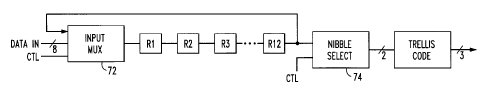
Figure 10 is a nibble select circuit 56 which may be used in the present
invention receives
zo a shream of digital data (DATA IN). A hellis encoding circuit may include
an input multiplexes
72 which loads the first of a series of twelve registers R1,R12 with data from
either an input
multiplexes 72, from the first of a series of twelve registers R1,R12, or from
the contents of the last
register in the series (R12) so as to cause all of the registers to cycle
through. At each bit selection
time, the contents of the last register (R12) are presented to a nibble select
circuit 74 which selects
15 two of the bits from the last register R12 in accor dance with the
preselected protocol. As each
nibble is selected from the last register, the contents of the registers are
cycled one register at a
timca, so that all of the twelve bytes within a segment are provided to the
nibble select circuit 74,
in t<zrn, a total of four times. When all of the bits of the twelve words have
been output from the
nibble select circuit 74, the input multiplexes 72 loads new data into the
twelve registers R1,R12
2o to encode the next segment of data.
Still another embodiment of a trellis encoder circuit is shown in Figure 11 in
which an
input data stream (DATA IN) is directed by a first multiplexes 82 to twelve
parallel registers
R1,R12. Once the registers are loaded, nibble select circuits 84 associated
with each of the storage
registers R1,R12 will select two data bits from their associated storage
registers R1,R12 and
2s provide the selected bits to an associated trellis encoder 86. Each trellis
encoder 86 encodes the
received bits in accordance with the predetermined encoding scheme and
provides the three
encoded bits to the input of an output multiplexes 88. The output multiplexes
selects the encoded
bits from the appropriate trellis encoder 86 in accordance with the protocol.
Note that the trellis
encoder of the embodiment in Figure 11 requires a depth of 1 whereas the
trellis encoders of
3o Figure 10 requires a depth of 12 if the trellis encoding scheme of the
standard DTV system is
being used.
14
CA 02233235 1998-03-27
It is well known that signal amplifiers often introduce non-linearities into
the signals
beirug amplified. To linearize signals which are to be amplified by such non-
linear amplifiers, it
is allso well known to pre-distort the input signal in a manner which is
opposite to the non-
linearity effects expected to be applied by the amplifier. Figure 12 is
(showing the amplitude of
s the signal versus frequency), an input signal having the form in Figure
12(A) will be pre-distorted
(or pre-corrected) by a transfer function as shown in Figure 12(B). After the
amplifier applies the
amplification effect shown in Figure 12(C) to the pre-corrected input signal,
the corrected,
amplified signal form is obtained, as shown in Figure 12(D). For further
explanation, in Figure
13 is depicted the same signals and effects as shown in Figure 12, this set of
drawing figures
io beircg shown in the frequency domain.
It has been found that known precorrection methods are usually limited to the
amplifier's
frequency response and the system band width. Pre-correction products which
have been used
to cancel the amplifier's distortions are modified in phase and amplitude by
the amplifier's input
circuits. These changes in the phase and amplitude limit the cancellation of
the distorting
is products in the amplifier. For example, the input circuits of a typical
amplifier often have the
amplitude and phase responses shown in Figure 14 over the frequency bands of
interest. These
amplitude and phase changes prevent the precorrection from cancelling all of
the unwanted
distortion of the amplifier. The resultant signals which are usually obtained
in such a circuit are
shown in Figure 15, a frequency domain series of drawings. Note the sidelobes
of frequency
2o elements caused by the uncorrected distortion.
One means for eliminating the unwanted non-linearities is to insert an
amplitude and
phase corrector between the prior art pre-correction and the non-linear
amplifier. The corrector
is adjusted so that its amplitude and phase responses are the inverse of the
amplitude and phase
responses of the non-linear amplifier.
2s Figure 16 is a circuit which can carry out the improved amplifier system
response that
may include a non-linear amplifier 170 and its associated amplifier input
circuits 166 and
amplifier output circuits 172. A precorrection circuit for amplitude versus
input (i.e., a linearity
corrector) 164 and for phase versus input (i.e., a phase corrector) 162 may
adjust for non-
linearities in a conventional fashion for the par ticular amplifier 170 and
the frequency ranges of
so interest. A frequency response and phase corrector 166 is placed between
the linearity corrector
164 and the amplifier input circuits 168 and is adjusted to compensate for the
inputs circuits so
CA 02233235 1998-03-27
6-305
that the net result of the cascaded pair of elements (corrector 166 and
circuits 168) is unity. In this
way, the precorrection signal can be fully compensated in the non-linear
amplifier 170.
Note that in the circuit of Figure 16, the phase corrector 162 precedes the
linearity
corrector 164. This is the preferred configuration of these correctors because
if these correctors
are reversed in order, the adjustment of the amplitude pre-correction would
cause undesired
changes in the phase pre-correction. These undesired changes can be
elimixiated; however, the
adjustment of the circuit to eliminate the effects of the undesired
interaction is made more
difficult.
The amplifier output circuits 172 of the non-linear amplifier 170 will often
also modify the
io ove:rall system frequency and phase response. To control this effect, a
frequency response
corrector 160 can be added to correct the overall system for transparency in
frequency and phase
response.
The frequency response correctors 160 and 166 may each be realized in
piecewise linear
correction circuits which can individually modify a signal's frequency
response and group delay
(or phase) response over a specified frequency range. These correctors should
be capable of: (1)
modifying amplitude versus frequency independently of phase (delay); and (2)
modifying phase
(delay) versus frequency (so called "group delay"). In a prefered embodiment,
the frequency
response correctors would implement these stated capabilities independently of
each other.
The phase corrector 162 may be realized in a piecewise linear correction
circuit which can
2o modify a signal's phase transfer function as a function of the input level.
The linearity corrector
164 may be realized by a conventional piecewise linear correction circuit
which can modify a
signal's linearity transfer function as a function of the input level. The
amplifier used in the
cirmit of Figure 16 may be any device intended to increase the level of an
input signal to a higher
level but generally has non-linearities or discontinuities in its transfer
function. Such an amplifier
may be solid state (such as a bipolar, MOSFET, LDMOS, silicon carbide, etc.)
or may be a vacuum
tuba (such as an IOT, tetrode, klystron, etc.). The amplifier input circuits
168 may typically
inchude input circuits to the amplifier such as input matching circuits,
filters, cavities, circulators,
etc. The amplifier output circuits 172 may typically include output circuits
from the amplifier
such as output matching circuits, filters, cavities, circulators, etc.
3o The set of correctors used in this aspect of the present invention would be
designed
starting with the phase corrector 162 and linearity corrector 166. Such
corrector circuits can be
16
CA 02233235 1998-03-27
6-305
designed conventionally to produce a desired predistorted signal inversely
matching the
abnormalities of the amplifier. Having designed the linearity and phase
correctors, the frequency
response corrector which comes after the linearity corrector can next be
designed as it will correct
for the frequency related errors caused by the amplifier input circuits.
Finally, the frequency
s response corrector at the beginning of the signal flow can be designed to
obviate errors in the
overall transfer function including the amplifier output circuits.
Figure 17 shows in which elements is common to the elements of Figure 16 have
been
provided with a common reference numeral, it is known that pre-correction in
prior art systems
is often accomplished at an intermediate frequency. The block diagram of this
aspect of the
io present invention may be modified as shown in Figure 17 where a frequency
mixer (or translator)
174 is placed between the precorrection elements and the non-linear amplifier
170. The mixer 174
may be supplied with a signal from a frequency reference 176 to translate the
signal being
amplified to a new frequency. The frequency reference 176 may include an
oscillator, tuned
circuit, external reference, or any conventional means or circuit to provide a
reference frequency.
15 The tight frequency control requirements which are to be levied upon DTV
broadcasters
to ensure a minimum of interference with other channels requires that special
attention be given
to tile effects of intermodulation products and frequency stability and
control. One system for
obti~ining satisfactory frequency control is illustr ated in the functional
block diagrams of Figures
18 and 19, which represent a typical site at which the television signals are
generated (such as a
2o studio) [Figure 18] and at which they are broadcast (such as a transmitter
site)[Figure 19]. Figure
18 ;shows television signals, STUDIO A/ V, from multiple and alternative
sources may be
provided to a conventional MPEG-2 encoder 180 which encodes the signals in a
conventional
fasl-aon using an external clock reference 182. The clock reference 182 may be
any highly stable
clock source, particularly a clock source which can be readily received at
remote locations, such
25 as a. GPS signal. The encoder 180 may provide an internal decoder so as to
provide a monitor
signal to a local audio-visual monitor 184. The encoded television signals)
are provided to a
"Gr;~nd Alliance" transport mechanism 186 which will format the incoming MPEG-
2 signal into
the proper format needed for the "transport layer" of the Grand Alliance
system. Alternatively,
the GA transport mechanism may receive (through a selectable switch) a signal
from an external
3o MP:EG-2 signal generator. The transport formatted signal may be provided to
a multiplexes 188
which multiplexes the transport formatted signal with other data and provides
the multiplexed
17
CA 02233235 1998-03-27
6-305
data to a transmission facility 190 for tr ansmission to a broadcast
transmitter site. Along a
somewhat parallel path, a "standard television" video signal or signals may be
converted to a
digital form by an analog to digital converter and the digitized video signal,
along with its
corresponding digital audio signal, may be provided to a NTSC 4/1 compressor
194. The
s compressed digital NTSC signal is provided to the multiplexer 1888 for
multiplexing with the
transport formatted signal and for transmission by the transmission facility
190. Each of the
encoder 180, transport mechanism 186, multiplexer 188, A/ D 192 and compressor
194 is locked
to the common clock reference 182. If the clock reference is taken from the
well-known Global
Positioning Satellite system (or any similar available, stable system), the
studio site can us the 1
io MEfz reference signal provided by the satellite system. Thus, both the DTV
signal (generated by
the transport mechanism 186) and the digital NTSC signal are locked for
efficient digital
transmission to the transmitter site. Because the DTV signal is locked to the
common reference
clock, multiplexing may be done in a synchronous mode with the digital NTSC
signal.
Figure 19 shows when the multiplexed signal arrives at the transmitter site,
it may be
is dennultiplexed by a demultiplexer (which may use any Forward Error
Correction signals
provided by the transmission facility 190) and provided as two data streams,
DTV and NTSC.
They DTV signal may be formatted for DTV broadcast and amplified by an exciter
200, power
amplified and upconverted, and ultimately broadcast through a suitable antenna
204. The NTSC
signal may be decoded to baseband by a NTSC decoder 208 and broadcast through
conventional
2o means. The demultiplexer 198, exciter 200, PA & Upconverter 202 and the
NTSC decoder 208
ma~;~ each be locked to a common clock reference 212.
The clock reference 212 at the transmitter site is optimally selected to be
common to the
clock reference 182 used at the studio site [Figure 18]. For example, both
sites could use the same
Gl'S reference signal. By using the same reference signal (such as the GPS 10
MHz signal), the
2s DT'V signal and the NTSC signal are locked to the same stable source. As a
result, the NTSC
chroma signal (at 3.58 MHz) is locked to a stable frequency source which will
reduce the
likelihood and/or severity of interference between the transmitted DTV pilot
signal and the
transmitted NTSC chroma signal.
Other stable clock reference signals can be used in common between the studio
site and
3o the transmitter site to achieve the advantages of the present invention.
For example, if the studio
site is sufficiently proximate to the transmitter site, the STL transmission
can be eliminated and
18
CA 02233235 1998-03-27
6-305
the clock signal can be carried by conventional means between the studio and
the transmitter.
If desired, fewer than all of the components shown as being related to the
clock reference
(CL,K REF) in Figures 18 and 19 need to be tied to a single (or related) clock
reference. The
improvements in adjacent and co-channel interference obtained from the use of
this embodiment
s of dhe present invention can be obtained if only the DTV exciter 200 and the
transmitter (PA and
Upconvert 202) use a common clock reference. In addition, the advantages of
the present
invention can be utilized more broadly by using a common clock reference at
plural sites. If
plural exciters and transmitters use a common stable reference, such as a
satellite signal, each
could generate a NTSC and DTV signal which would reduce interference not only
with the co-
io generated television signals but also with other signals generated at other
sites whose assigned
channels may have otherwise caused interference from frequency inaccuracies.
An exciter circuit for receiving input television digital signals from a
source and
converting the television digital signals W to a standard format for
broadcasting by television
traxismitter power amplification stages via an antenna, comprises a data
recovery circuit for
is exWacting data and clock signals from the input television digital signal
for outputting the
ext~~acted the digital clock signals for separately outputting the digital
clock signals and the
digiital data signals, a randomiser circuit for altering the order of the
extracted digital data signals
in accordance with digital television standards, an encoder circuit for
encoding the digital data
signals into packets synchronised to receive the digital data signals at the
input television digital
2o signal rate, an interleaver circuit for performing a convolutional
interleaving of the packets of
digiital data signals synchronised to receive packets of digital data signals
at a second layer rate,
an encoder circuit for encoding the convoluted interleaved digital data
signals with a trellis code
according to digital television standards, a sync insertion circuit for
inserting segment and field
sync signal into the encoded digital data signals, a filter circuit for
limiting the spectrum of the
zs encoded digital data signals to the digital television standard, a signal
insertion circuit for
inserting the extracted digital clock signal into the output of the filter
circuit, a digital to
analogue conversion circuit for converting the digital data signals and the
digital clock signals
into analogue signals in form for transmission by the power amplifier stage,
and a rate controler
for receiving input signals and controlling output signals even in absence of
the input signal.
3o A trellis encoder circuit comprises receiving means to receive a stream of
digital bits,
loading means for loading M successive data bits into a first data register
from one of said
19
CA 02233235 1998-03-27
6-305
receiving means and another data register, N successive data registers, each
successive data
register connected in series with one of said successive data registers and
said first data register,
mewls for cycling the digital bits in the last of said N successive data
registers into said first data
register, first multiplexer means for selecting one of plural sets of digital
bits from said last data
s register, means for trellis encoding said one set of digital bits and
providing a trellis encoded set
of digital bits, and logic means for cycling the digital bits in said
successive registers until all the
digital bits have been trellis encoded and for reloading said successive
registers from said stream
of digital bits wherein N and M are integers greater than 1.