Note: Descriptions are shown in the official language in which they were submitted.
CA 02233238 1998-03-26
W O 97/12030 PCT~US96/14353
DESCRIPTION
A~paratus and Methods for Active Proqrammable
Matrix Devices
Field of the Invention
This invention relates to devices and systems for
performing multi-step molecular biological type diagnos~ic
analyses in multiplex formats. More particularly, the
molecular biological type analyses include various nucleic
acid hybridizations reactions and associated biopolymer
synthesis. Additionally, antibody/antigen reactions and
other clinical diagnostics can be performed.
Related Application Information
This application is a continuation-in-part of appli-
cation Serial No. 08/304,657, filed September 9, 1994,
entitled "AUTOMATED MOLECULAR BIOLOGICAL DIAGNOSTIC
SYSTEM," which is a continuation-in-part of application
Serial No. 08/271,882, filed July 7, 1994, entitled "SELF-
ADDRESSABLE SELF-ASSEMBLING MICROELECTRIC SYSTEMS AND
DEVICES FOR MOLECULAR BIOLOGICAL ANALYSIS AND DIAGNOS-
TICS," which is a continuation-in-part of Serial No.
07/146,504, filed November 1, 1993, entitled "ACTIVE
PROGRAMMABLE ELECTRONIC DEVICES FOR MOLECULAR BIOLOGICAL
ANALYSIS AND DIAGNOSTICS."
Backqround of the Invention
Molecular biology comprises a wide variety of
techniques for the analysis of nucleic acid and protein.
Many of these techniques and procedures form the basis of
clinical diagnostic assays and tests. These techniques
include nucleic acid hybridization analysis, restriction
enzyme analysis, genetic sequence analysis, and the
separation and purification of nucleic acids and proteins
(See, e.g., J. Sambrook, E. F. Fritsch, and T. Maniatis,
Molecular Cloninq: A Laboratory Manual, 2 Ed., Cold
CA 02233238 1998-03-26
W O 97/12030 PCT~US96/14353
spring Harbor Laboratory Press, Cold Spring Harbor, Mew
York, 1989).
Most of these techniques involve carrying out
numerous operations (e.g., pipetting, centrifugations,
electrophoresis)on a large number of samples. They are
often complex and time consuming, and generally require a
high degree of accuracy. Many a technique is limited in
its application by a lack of sensitivity, specificity, or
reproducibility. For example, these problems have limited
many diagnostic applications of nucleic acid hybridization
analysis.
The complete process for carrying out a DNA hybrid-
ization analysis for a genetic or infectious disease is
very involved. Broadly speaking, the complete process may
be divided into a number of steps and substeps (see Figure
1). In the case of genetic disease diagnosis, the first
step involves obtaining the sample (blood or tissue).
Depending on the type of sample, various pre-treatments
would be carried out. The second step involves disrupting
or lysing the cells, which then release the crude DNA
material along with other cellular constituents. Gener-
ally, several sub-steps are necessary to remove cell
debris and to purify further the crude DNA. At this point
several options exist for further processing and analysis.
One option involves denaturing the purified sample DNA and
carrying out a direct hybridization analysis in one of
many formats (dot blot, microbead, microliter plate,
etc.). A second option, called Southern blot hybrid-
ization, involves cleaving the DNA with restriction
enzymes, separating the DNA fragments on an electrophoret-
ic gel, blotting to a membrane filter, and then hybrid-
izing the blot with specific DNA probe sequences. This
procedure effectively reduces the complexity of the
genomic DNA sample, and thereby helps to improve the
hybridization specificity and sensitivity. Unfortunately,
this procedure is long and arduous. A third option is to
carry out the polymerase chain reaction (PCR) or other
CA 02233238 1998-03-26
W O 97/12030 PCT~US96/14353
amplification procedure. The PCR procedure amplifies
(increases) the number of target DNA sequences. Amplifi-
cation of target DNA helps to overcome problems related to
complexity and sensitivity in genomic DNA analysis. All
these procedures are time consuming, relatively compli-
cated, and add significantly to the cost of a diagnostic
test. After these sample preparation and DNA processing
steps, the actual hybridization reaction is performed.
Finally, detection and data analysis convert the
hybridization event into an analytical result.
The steps of sample preparation and processing have
typically been performed separate and apart from the other
main steps of hybridization and detection and analysis.
Indeed, the various substeps comprising sample preparation
and DNA processing have often been performed as a discrete
operation separate and apart from the other substeps.
Considering these substeps in more detail, samples have
been obtained through any number of means, such as
obtaining of full blood, tissue, or other biological fluid
samples. In the case of blood, the sample is processed to
remove red blood cells and retain the desired nucleated
(white) cells. This process is usually carried out by
density gradient centrifugation. Cell disruption or lysis
is then carried out, preferably by the technique of
sonication, freeze/thawing, or by addition of lysing
reagents. Crude DNA is then separated from the cellular
debris by a centrifugation step. Prior to hybridization,
double-stranded DNA is denatured into single-stranded
form. Denaturation of the double-stranded DNA has gener-
ally been performed by the techniques involving heating
(>Tm), changing salt concentration, addition of base(NaOH), or denaturing reagents (urea, formamide, etc.).
Workers have suggested denaturing DNA into its single-
stranded form in an electrochemical cell. The theory is
stated to be that there is electron transfer to the DNA at
the interface of an electrode, which effectively weakens
the double-stranded structure and results in separation of
CA 02233238 1998-03-26
W O 97/12030 PCTAUS96/14353
the strands. See, generally, Stanley, "DNA Denaturation
by an Electric Potential", U.K. patent application
2,247,889 published March 18, 1992.
Nucleic acid hybridization analysis generally
involves the detection of a very small number of specific
target nucleic acids (DNA or RNA) with an excess of probe
DNA, among a relatively large amount of complex non-target
nucleic acids. The substeps of DNA complexity reduction
in sample preparation have been utilized to help detect
low copy numbers (i.e. 10,000 to 100,000) of nucleic acid
targets. DNA complexity is overcome to some degree by
amplification of target nucleic acid sequences using
polymerase chaln reaction (PCR). (See, M.A. Innis et al,
PCR Protocols: A Guide to Methods and A~lications,
Academic Press, 1990). While amplification results in an
enormous number of target nucleic acid sequences that
improves the subsequent direct probe hybridization step,
amplification involves lengthy and cumbersome procedures
that typically must be performed on a stand alone basis
relative to the other substeps. Substantially complicated
and relatively large equipment is required to perform the
ampli~ication step.
The actual hybridization reaction represents the most
important and central step in the whole process. The
hybridization step involves placing the prepared DNA
sample in contact with a specific reporter probe, at a set
of optimal conditions for hybridization to occur to the
target DNA sequence. Hybridization may be performed in
any one of a number of formats. For example, multiple
sample nucleic acid hybridization analysis has been
conducted on a variety of filter and solid support formats
(See G. A. Beltz et al., in Methods in Enzvmoloqy, Vol.
100, Part B, R. Wu, L. Grossman, K. Moldave, Eds.,
Academic Press, New York, Chapter 19, pp. 266-308, 1985).
One format, the so-called "dot blot" hybridization,
involves the non-covalent attachment of target DNAs to
filter, which are subsequently hybridized with a
CA 02233238 1998-03-26
W O 97/12030 PCTAJS96/14353
radioisotope labelled probe(s). "Dot blot" hybridization
gained wide-spread use, and many versions were developed
(see M. ~. M. Anderson and B. D. Young, in Nucleic Acid
Hvbridization - A Practical Approach, B. D. Hames and S.
J. Higgins, Eds., IRL Press, Washington, D.C. Chapter 4,
pp. 73-111, 1985). It has been developed for multiple
analysis of genomic mutations (D. Nanibhushan and D.
Rabin, in EPA 0228075, July 8, 1987) and for the detection
of overlapping clones and the construction of genomic maps
(G. A. Evans, in US Patent Number 5,219,726, June 15,
1993)-
New techniques are being developed for carrying outmultiple sample nucleic acid hybridization analysis on
micro-formatted multiplex or matrix devices (e.g., DNA
chips) (see M. Barinaga, 253 Science, pp. 1489, 1991; W.
Bains, 10 Bio/Technology, pp. 757-758, 1992). These
methods usually attach specific DNA sequences to very
small specific areas of a solid support, such as micro-
wells of a DNA chip. These hybridization formats are
micro-scale versions of the conventional "dot blot" and
"sandwich" hybridization systems.
The micro-formatted hybridization can be used to
carry out "sequencing by hybridization" (SBH) (see M.
Barinaga, 253 Science, pp. 1489, 1991; W. Bains, 10
Bio/Technology, pp. 757-758, 1992). SBH makes use of all
possible n-nucleotide oligomers (n-mers) to identify n-
mers in an unknown DNA sample, which are subsequently
aligned by algorithm analysis to produce the DNA sequence
(R. Drmanac and R. Crkvenjakov, Yugoslav Patent Applica-
tion #570/87, 1987; R. Drmanac et al., 4 Genomics, 114,1989; Strezoska et al., 88 Proc. Natl. Acad. Sci. USA
10089, 1992; and R. Dramanac and R. B. Crkvenjakov, U.S.
Patent #5,202,231, April 13, 1993).
There are two formats for carrying out SBH. The
first format involves creating an array of all possible n-
mers on a support, which is then hybridized with the
target sequence. The second format involves attaching the
,
CA 02233238 1998-03-26
W O 97/12030 PCTnJS96/14353
target sequence to a support, which is sequentially probed
with all possible n-mers. Both ~ormats have the ~1ln~men-
tal problems o~ direct probe hybridizations and additional
difficulties related to multiplex hybridizations.
Southern, United Klngdom Patent Application GB
8810400, 1988; E. M. Southern et al., 13 Genomics 1008,
1992, proposed using the first format to analyze or
sequence DNA. Southern identified a known single point
mutation using PCR amplified genomic DNA. Southern also
described a method for synthesizing an array of
oligonucleotides on a solid support for SBH. However,
Southern did not address how to achieve optimal stringency
condition for each oligonucleotide on an array.
Concurrently, Drmanac et al., 260 Science 1649-1652,
1993, used the second format to sequence several short
(116 bp) DNA sequences. Target DNAs were attached to
membrane supports ("dot blot" format). Each filter was
sequentially hybridized with 272 labelled 10-mer and 11-
mer oligonucleotides. A wide range of stringency
condition was used to achieve speci~ic hybridization for
each n-mer probe; washing times varied from 5 minutes to
overnight, and temperatures ~rom 0~C to 16~C. Most probes
required 3 hours of washing at 16~C. The filters had to
be exposed for 2 to 18 hours in order to detect hybridiza-
tion signals. The overall ~alse positive hybridizationrate was 5% in spite o~ the simple target sequences, the
reduced set of oligomer probes, and the use of the most
stringent conditions available.
A variety of methods exist for detection and analysis
of the hybridization events. Depending on the reporter
group (~luorophore, enzyme, radioisotope, etc.) used to
label the DNA probe, detection and analysis are carried
out fluorometrically, colorimetrically, or by autoradiog-
raphy. By observing and measuring emitted radiation, such
as ~luorescent radiation or particle emission, information
may be obtained about the hybridization events. Even when
detection methods have very high intrinsic sensitivity,
CA 02233238 1998-03-26
W O 97/12030 PCT~US96/14353
detection of hybridization events is difficult because of
the background presence of non-specifically bound materi-
als. A number of other factors also reduce the sensitivity
and selectivity of DNA hybridization assays.
In conventional fluorometric detection systems, an
excitation energy o~ one wavelength is delivered to the
region of interest and energy of a different wavelength is
reemitted and detected. Large scale systems, generally
those having a region of interest o~ two millimeters or
greater, have been manufactured in which the quality of
the overall system is not inherently limited by the size
requirements of the optical elements or the ability to
place them in optical proximity to the region of interest.
However, with small geometries, such as those below 2
millimeters, and especially those on the order o~ 500
microns or less in size of the region of interest, the
conventional approaches to fluorometer design have proved
inadequate. Generally, the excitation and emission
optical elements must be placed close to the region of
interest. Preferably, a focused spot size is relatively
small, often requiring sophisticated optical designs.
Further, because it is usually desirable to maximize the
detectable area, the size of the optical components
required to achieve these goals in relation to their
distance from the region of interest becomes important,
and in many cases, compromises the performance obtained.
Accordingly, a need exists for an improved fluorescent
detection system.
Attempts have been made to combine certain processing
steps or substeps together. For example, various
microrobotic systems have been proposed for preparing
arrays of DNA probe on a support material. For example,
Beattie et al., in The 1992 San Dieqo Conference: Genetic
Recoqnition, November, 1992, used a microrobotic system to
deposit micro-droplets containing specific DNA sequences
into individual microfabricated sample wells on a glass
substrate.
CA 02233238 1998-03-26
W O 97/12030 PCTAJS96/14353
Generally, the prior art processes have been
extremely labor and time intensive. For example, the PCR
amplification process is time consuming and adds cost to
the diagnostic assay. Multiple steps requiring human
intervention either during the process or between
processes is suboptimal in that there is a possibility of
contamination and operator error. Further, the use of
multiple machines or complicated robotic systems for
performing the individual processes is o~ten prohlbitive
except for the largest laboratories, both in terms of the
expense and physical space requirements.
As is apparent from the preceding discussion,
numerous attempts have been made to provide ef~ective
techniques to conduct multi-step, multiplex molecular
biological reactions. However, for the reasons stated
above, these techniques are "piece-meal" and limited.
These various approaches are not easily combined to form
a system which can carry out a complete DNA diagnostic
assay. Despite the long-recognized need for such a system,
no satisfactory solution has been proposed previously.
Summary of the Invention
The present invention relates to the design, fabrica-
tion, and uses of a self-addressable self-assembling
microelectronic devices and systems which can actively
carry out controlled multi-step processing and multiplex
reactions in a microscopic ~ormats. These reactions
include, but are not limited to, most molecular biological
procedures, such as nucleic acid hybridization, anti-
body/antigen reaction, and related clinical diagnostics.
In addition, the claimed devices and systems are able to
carry out multi-step combinatorial biopolymer synthesis,
including, but not limited to, the synthesis of different
oligonucleQtides or peptides at specific micro-locations
on a given device.
The claimed devices and systems are fabricated using
both microlithographic and micro-machining techniques.
CA 02233238 1998-03-26
W O 97/12030 PCT/US96/14353
The basic device has a matrix of addressable microscopic
locations on its surface; each individual micro-location
is able to control electronically and direct the transport
and attachment of specific binding entities (e.g., nucleic
acids, enzyme~, antibodies) to itself. All micro-
locations can be addressed with their specific binding
entities. The self-addressing process requires minimal
outside intervention in terms of fluidics or mechanical
components.
The device is able to control and actively carry out
a variety of assays and reactions. Analytes or reactants
can be transported by free field electrophoresis to any
specific micro-location where the analytes or reactants
are effectively concentrated and reacted with the specific
binding entity at the micro-location. In the case of
hybridization analysis, the sensitivity for detecting a
specific analyte or reactant is improved because hybrid-
ization reactants are concentrated at a specific micro-
scopic location. Any un-bound analytes or reactants can
be removed by reversing the polarity of a micro-location.
Thus, the device also improves the specificity of the
reactions. Basic devices for nucleic acid hybridization
and other analyses are alternatively referred to as APEX
devices, which stands for addressable programmable
electronic matrix.
In one aspect of this invention, the APEX device is
utilized with a fluidic system in which a sample is flowed
over the APEX device during operation. In the preferred
embodiment, the fluidic system includes a flow cell and a
liquid waste containment vessel. The sample is provided
to the input to the flow cell and directed across the
active areas of the APEX system. Preferably, a defined
volume is provided within the flow cell, preferably in the
range from 5 to 10 microliters. A flowing sample over the
active detection device provides important advantages in
the hybridization analysis of dilute, concentrated and/or
relatively complex DNA samples. For example, if the total
CA 02233238 1998-03-26
W O 97/12030 PCT/US96/1~353
sample volume is relatively large compared to the same
chamber volume, flowing of the sa~ple provides more
complete analysis of the entire sample. Alternatively,
where the sample volume is relatively small, and/or the
DNA is relatively concentrated, dilution is indicated in
order to reduce the viscosity of the sample.
In another aspect of the invention, additional
processing steps or substeps may be performed in sequence
with a "system". The system is an integrated arrangement
of component devices. Each component device is appropri-
ately designed and scaled to carry out a particular
function. In its most complete embodiment, a system may
perform all aspects of sample preparation, hybridization
and detection and analysis. In this fullest form, the
sample is first prepared, such as by an electronic cell
sorter component. Generally, electronic refers more
specifically to the ability of the component device to
electrophoretically transport charged entities to or from
itself. Further DNA processing and complexity reduction
may optionally be performed by a crude DNA selector
component, and a restriction fragment selector component.
The final processed target DNA is transported to the
analytical component where electronic hybridization
analysis is carried out in a microscopic multiplex format.
This analytical component device is also referred to as
the APEX or analytical chip. Associated detection and
lmage analysis components provide the results.
Within the system materials may optionally be trans-
ported between components (devices) by free field electro-
phoresis, channelling, fluidics or other techniques.Optionally, electronic reagent dispenser components can
provide electrophoretic transport of reagents to the
various processing components of the system. Optionally,
an electronic waste disposal system may be formed by
providing an electrode and charged matrix material that
attracts and holds charged waste products. Optionally, an
electronic DNA fragment storage system can serve to
CA 02233238 1998-03-26
W O 97/12030 PCT~US96/14353
temporarily hold other DNA fragments for later hybridiza-
tion analysis.
In one aspect of this invention, genomic DNA
complexity reduction is per~ormed by processes that
isolate those speci~ic DNA fragments containing the
desired target sequence from the bulk of the DNA material
that lacks the desired target sequence. Crude DNA can be
transported and captured on a support material. The bound
DNA can then be severed using appropriate restriction
enzymes. A~ter severing, the DNA ~ragments can be
transported to a component device that selectively
hybridizes specific DNA fragments. Those fragments that
contain the actual target sequences to be analyzed can be
selectively released, via further restriction enzyme
cleavage, and transported to the analytical component
(APEX chip) of the system. Optionally, thls procedure may
be repeated for other fragments containing other target
sequences.
A controller for the device (or system) provides for
individual control of various aspects of the device. When
an APEX device or chip containing addressable microscopic
locations is utilized, the controller permits individual
microlocations to be controlled electronically so as to
direct the transport and attachment of speci~ic binding
entities to that location. The device may carry out
multi-step and multiplex reactions with complete and
precise electronic control, preferably under control o~
a microprocessor based component. The rate, specificity,
and sensitivity of multi-step and multiplex reactions are
greatly improved at the speci~ic microlocations on the
device. The controller interfaces with a user via
input/output devices, such as a display and keyboard
input. Pre~erably, a graphical user interface is adapted
for ease of use. The input/output devices are connected
to a controller, which in turn controls the electrical
status of the addressable elec~ronic locations on the
system. Specifically, the controller directs a power
CA 02233238 1998-03-26
W O 97/12030 PCT~US96/1~353
supply/waveform generator to generate the electronic
status of the various microlocations. Optionally, an
interface is used between the power supply/waveform
generator and the APEX device or system. The lnterface
preferably comprises a bank of relays subject to the
controller via a multifuncti~n input/output connection.
The relays preferably serve to connect the power
supply/waveform generator to the APEX device by
controlling the connection as to its polarity, the
presence or absence of a connection and the amount of
potential or current supply to the individual location.
The controller preferably controls the illumination source
directed at the hybridization system. A detector, image
processing and data analysis system are optically coupled
to the APEX device. In the preferred embodiment, a
fluorescent microscope receives and magnifies the image
from the hybridization events occurring on the various
micro-locations of the device. The emissions are optically
filtered and detected by a charge coupled device (CCD)
array or microchannel plate detector. The image is then
stored and analyzed. Preferably, the results are
displayed to the user on the monitor.
In one aspect of this invention, an improved
apparatus for the detection of fluorescence in small
geometry systems is utilized. In the preferred
embodiment, a light transfer member, such as an optical
fiber, is disposed within a light guide path disposed
between the region of interest and the detector. In the
most preferred embodiment, a fiber optic is coaxially
arranged in a liquid light guide. An excitation source,
such as a laser, provides radiation through optics such
that the excitation fiber delivers the excitation
radiation to the region of interest. Preferably, the
excitation fiber is disposed axially within the return
light guide path, at least at the proximal end adjacent
the region of interest. The return path pre~erably
comprises a liquid light guide preferably including optics
CA 02233238 1998-03-26
W O 97/12030 PCTAJS96/14353
to receive emission from the region of interest, and to
transfer that emission through the light guide to the
detector.
In another aspect of this invention, the hybridiza-
tion system is formed having a plurality of microlocationsformed atop a substrate containing control electronics.
Specifically, swltching circuits are provided to address
individually the microlocations. The electrical connec-
tions are made via the backside relative to where sample
contact is to be made. Additionally, an optical pathway,
such as a waveguide, i8 disposed beneath the microlocation
to permit backside access to the microlocation. Optical
excitation, if necessary, may be directed to the
microlocation via the waveguide. Detection of emitted
radiation may be detected via the backside waveguide. In
yet another aspect of this invention, a sample cont~;nm~nt
system is disposed over the system, particularly the
hybridization matrix region. In the preferred embodiment,
the matrix hybridization region (including sample contain-
ment component) is adapted for removal from the remainderof the device providing the electronic control and detec-
tor elements.
In another aspect of this invention, improved
processes for forming a matrix hybridization system are
described. In one process, a substrate, such as silicon,
is formed with an insulating layer, such as a thick oxide.
Conductive microlocations are formed, such as by
deposition of metal (e.g., aluminum or gold) that is then
patterned, such as by conventional photo-lithographic
techni~ues. An insulating coating is formed, such as TEOS
formed by PECVD. Optionally, a nitride passivation
coating is formed over the TEOS layer. Openings to the
microelectrode are formed through the nitride and glass.
Optionally, adhesion improving materials such as titanium
tungsten may be utilized in connection with the metal
layer to promote adhesion to the oxide and/or glass. In
yet a further improvement, wells may be formed atop of the
CA 02233238 1998-03-26
WO 97/12030 PCT~US96/14353
14
electrode by undercutting a nitride layer disposed on an
oxide layer supported by the substrate.
Electronic control of the individual microlocations
may be done so as to control the voltage or the current.
When one aspect is set, the other may be monitored. For
example, when voltage is set, the current may be moni-
tored. The voltage and/or current may be applied in a
direct current mode, or may vary with time. For example,
pulsed currents or DC biases may be advantageously
utilized. The pulsed system may be advantageously uti-
lized with the fluidic system, especially the flow cell
design. By coordinating the pulse sequence and flow rate,
the sample can be more effectively interrogated throughout
the sample volume. Additionally, even for non-flow
situations, such as where there are relatively high
amounts of non-target material, e.g., DNA, which without
pulsing might overwhelm the activated test sites. Pulse
techniques generally result in higher target mobility
rates at higher ionic strength, reduced probe burn-out
effects, improved hybridization efficiencies, improved
discrimination of point mutations and enhanced DNA
fingerprinting.
In yet another aspect of this invention, it has been
surprisingly discovered that the fluorescence signal
obtained during the electronic denaturation of:DNA hybrids
is perturbed at or around electronic and power levels
which are associated with dehybridization. Specifically,
the fluorescence signal perturbation results in a rise or
spike in fluorescence intensity prior to dehybridization
of fluorescently labelled probes from a capture sequence
attached to an APEX pad. The power level, amplitude and
slope of this fluorescence spike provide analytical tools
for diagnosis. The combination of the fluorescence
perturbation with other measurements also indicative of
the hybridization match/mismatch state, such as
consideration of the electronic melting (50~ fluorescence
decrease during electronic stringency control) can in
CA 02233238 1998-03-26
W O 97/12030 PCTAUS96/14353
combination provide a more efficient and reliable
hybridization match/mismatch analysis.
It is yet another aspect of this invention to provide
for an improved DNA ~ingerprinting system using a
microelectronic device. Such a device would be utilized
to differentiate targets in the range from approximately
100 to approximately 3000 base pairs in size.
Fluorescently labelled fragments having a given length
would be attached to a capture probe at a test site. A
reverse potential would be applied to the test site in an
amount sufficient to determine the amount of binding
between the capture probe and the labelled ~ragment.
Generally, this would be by applying a reverse potential
at increasing current so as to result in dehybridization
of the targets at the site. Those DNA having longer
length will be selectively dehybridized at lower
electronic current levels. As such, the dehybridization
current level correlates with DNA size.
Accordingly, it is an object of this invention to
provide a system for the sample preparation, processing,
hybridization, detection and analysis of biological
materials.
It is yet a further object of this invention to
provide a system that combines multiple steps or substeps
within an integrated system.
It is yet a further object of this invention to
provide for an automated DNA diagnostic system.
It is yet another object of this invention to provide
~or an improved fluorescence detection system, especially
useful for small geometries.
It is yet another object of this invention to provide
for an integrated, disposable combination of a fluidic
system, such as a flow cell, and an active detection
device.
It is yet another object of this invention to provide
a system which is capable of manufacture using
CA 02233238 1998-03-26
W O 97/12030 PCT~US96/14353
conventional techniques, with high efficiencies and low
cost.
It is yet a further object of this invention to
provide an improved DNA fingerprinting and analysis system
which electronically discriminates between varying length
DNA fragments.
Brie~ Description of the Drawinqs
Fig. 1 shows the sequence of steps and substeps for
sample preparation, hybridization and detection and data
analysis.
Figs. 2A and 2B show the active, programmable matrix
system in cross-section (Fig. 2A) and in perspective view
(Fig. 2B).
Fig. 3 shows the active, programmable matrix system
structure at the metal mask layer.
Fig. 4 shows detail of the active, programmable
matrix system in plan view.
Fig. 5 shows a perspective view of a single
microlocation and electrical connection.
Fig. 6 shows a cross-sectional view of a fluidic
system including a flow cell in combination with the APEX
device.
Fig. 7 shows a plan view of a fluidic system in-
cluding a flow cell and liquid waste cont~-n~nt system in
combination with the diagnostic system on a PCMCIA board.
Fig. 8 shows a plan view of the system including an
electronic cell sorter matrix, DNA selectors and restric-
tion fragment selectors and hybridization matrix.
Fig. 9 shows a block diagram description of the
control system.
Fig. 10 shows user displays for various voltage and
current regimes.
Fig. 11 shows a cross-sectional view of a
fluorescence detection system useful for small geometry
systems.
-
CA 02233238 1998-03-26
W O 97/12030 PCT/US96/14353
Fig. 12A is a plot of the relative fluorescent
intensity as a function of applied power (microwatts) for
a 20-mer oligomer duplex (100% AT).
Fig. 12B is a plot of the relative fluorescent
5 intensity versus applied power (microwatt) ~or a l9-mer
oligomer duplex (53% GC).
Fig. 13A is a graph of the relative :Eluorescent
intensity versus applied power (microwatt) i~or a 20-mer
oligomer duplex (100% AT).
Fig. 13B is a plot of the relative fluorescent
intensity versus applied power (microwatt) for a l9-mer
oligomer duplex (53% GC).
Fig. 14A shows a cross-sectional view of a mismatched
test site having a capture probe, target DNA and a
15 reporter probe.
Fig. 14B is a cross-sectional view of target DNA and
a reporter probe with a associated fluorophore.
Fig. 14C is a graph of the fluorescent response
graphing the relative fluorescent intensity as a function
20 of time ~or a pulsed sequence.
Fig. 15A is a cross-sectional view of a matched test
site having a capture probe, target DNA and a reporter
probe with an intercalcated fluorophore.
Fig. 15B is a cross-sectional view of target DNA and
25 a reporter probe with an intercalcating fluorophore.
Fig. 15C is a graph of the fluorescent response
showing the relative fluorescence intensity as a function
of time for a pulsed sequence.
Fig. 16A-D are cross-sectional views of multiple test
30 sites of a electronic stringency control device utilized
- for DNA fingerprinting and analysis.
Detailed Descri~tion of the Invention
Figs. 2A and 2B illustrate a simplified version of
the active programmable electronic matrix hybridization
35 system for use with this invention. Generally, a
substrate lO supports a matrix or array of electronically
CA 02233238 l998-03-26
W O 97/12030 PCTAUS96/143j3
18
addressable microlocations 12. For ease of explanation,
the various microlocations in Fig. 2A have been labelled
12A, 12B, 12C and 12D. A permeation layer 14 is disposed
above the individual electrodes 12. The permeation layer
permits transport of relatively small charged entities
through it, but precludes large charged entities, such as
DNA, from contacting the electrodes 12 directly. The
permeation layer 14 avoids the electrochemical degradation
which would occur in the DNA by direct contact with the
electrodes 12. It further serves to avoid the strong,
non-specific adsorption of DNA to electrodes. Attachment
regions 16 are disposed upon the permeation layer 14 and
provide for specific binding sites for target materials.
The attachment regions 16 have been labelled 16A, 16B, 16C
and 16D to correspond with the identification of the
electrodes 12A-D, respectively.
In operation, reservoir 18 comprises that space above
the attachment regions 16 that contains ~he desired, as
well as undesired, materials for detection, analysis or
use. Charged entities 20, such as charged DNA are located
within the reservoir 18. In one aspect of this invention,
the active, programmable, matrix system comprises a method
for transporting the charged material 20 to any of the
specific microlocations 12. When activated, a
microlocation 12 generates the free field electrophoretic
transport of any charged functionalized specific binding
entity 20 towards the electrode 12. For example, if the
electrode 12A were made positive and the electrode 12D
negative, electrophoretic lines of force 22 would run
between the electrodes 12A and 12D. The lines of electro-
phoretic force 22 cause transport of charged binding
entities 20 that have a net negative charge toward the
positive electrode 12A. Charged materials 20 having a net
positive charge move under the electrophoretic force
toward the negatively charged electrode 12D. When the net
negatively charged binding entity 20 that has been
functionalized contacts the attachment layer 16A as a
CA 02233238 1998-03-26
W O 97/12030 PCT~US96tl4353
19
result o~ its movement under the electrophoretic force,
the functionalized specific binding entity 20 becomes
covalently attached to the attachment layer 16A.
The electrophoretic transport generally results from
applying a voltage which is sufficient to permit
electrolysis and ion transport within the system.
Electrophoretic mobility results, and a current flows
through the system, such as by ion transport through the
electrolyte solution. In this way, a complete circuit may
be formed via the current flow of the ions, with the re-
mainder of the circuit being completed by the conventional
electronic components, such as the electrodes and
controlled circuitry. By way of example, for an aqueous
electrolyte solution containing conventional material such
as sodium chloride, sodium phosphate, buffers and ionic
species, the voltage which induces electrolysis and ion
transport is greater than or equal to approximately 1.2
volts.
It is possible to protect the attachment layers which
are not subject to reaction, such as 16B and 16C by making
their corresponding electrodes 12B and 12C negative. This
results in electrophoretic lines o~ force emanating from
the attachment region 16B (only 16B will be discussed for
simplicity, the results being similar for 16C). The
electrophoretic force lines 24 serve to drive away nega-
tively charged binding entities 20 from the attachment
layer 16B and towards the attachment layer 16A. In this
way, a "force field" protection is formed around the
attachment layers 16 which it is desired to have nonreac-
tive with the charged molecules 20 at that time.
One highly advantageous result of this system is thatcharged binding materials 20 may be highly concentrated in
regions ad~acent to signal attachment layers 16. As can
be seen in perspective drawing Fig. 2B, if a individual
microlocation 26A is positively charged, and the remaining
microlocation are negatively charged, the lines of
electrophoretic force will cause transport of the net
CA 02233238 1998-03-26
W O 97/12030 PCT~US96/14353
negatively charyed binding entities 20 toward the
microlocation 26A. The microlocation 26A is intended to
depict the combination in Fig. 2A of the attachment layer
16, the permeation layer 14 and the underlying associated
electrode 12. In this way, a method for concentrating and
reacting analytes or reactants at any specific
microlocation on the device may be achieved. After the
attachment of the specific binding entities 20 to the
attachment layer 16, the underlying microelectrode 12 may
continue to function in a direct current (DC) mode. This
unique feature allows relatively dilute charged analytes
or reactant molecules ~ree in solution to be rapidly
transported, concentrated, and reacted in a serial or
parallel manner at any specific micro-location that is
maintained at the opposite charge to the analyte or
reactant molecules. This ability to concentrate dilute
analyte or reactant molecules at selected microlocations
26 greatly accelerates the reaction rates at these microl-
ocations 26.
After the desired reaction is complete, the electrode
12 may have its potential reversed thereby creating an
electrophoretic force in the direction opposite to the
prior attractive force. In this way, nonspecific analytes
or unreacted molecules may be removed from the
microlocation 26. Specific analytes or reaction products
may be released from any microlocation 26 and transported
to other locations for further analysis; or stored at
other addressable locations; or removed completely from
the system. This removal or deconcentration of materials
by reversal of the field enhances the discrimination
ability of the system by resulting in removal of
nonspecifically bound materials. By controlling the
amount of now repulsive electrophoretic force to nonspe-
cifically bound materials on the attachment layer 16,
electronic stringency control may be achieved. By raising
the electric potential at the electrode 12 so as to create
a field sufficient to remove partially hybridized DNA
,
CA 02233238 1998-03-26
W O 97/12030 PCT~US96/14353
21
sequences, thereby permitting identification of single
mismatched hybridizations, point mutations may be identi-
fied.
Operations may be conducted in parallel or in series
at the various attachment layers 16. For example, with
reference to Fig. 2A, a reaction may occur first at
attachment layer 16A utilizing the potentials as shown.
The potential at electrode 12A may be reversed, that is,
made negative, and the potential at the adjacent electrode
12B may be made positive. In this way, a series reactions
occurs. Materials that were not specifically bound to
attachment layer 16A would be transported by electropho-
retic force to attachment layer 16B. In this way, the
concentration aspect is utilized to provide high concen-
trations at that specific attachment layer then subject tothe positive electrophoretic force. The concentrated
materials may next be moved to an adjacent, or other,
attachment layer 16. Alternatively, multiple attachment
layers 16 may be deprotected in the sense that there is a
net electrophoretic force field emanating from the elec-
trode 12 through the attachment layer 16 out into the
reservoir 18. By deprotecting multiple attachment layer
16, multiplex reactions are performed. Each individual
site 26 may serve in essence as a separate biological
"test tube" in that the particular environment addressed
by a given attachment layer 16 may differ from those
environments surrounding the other attachment layers 16.
Fig. 3 shows a plan view of the metal mask layer for
an active programmable electronic matrix system. A
plurality of individual electrodes 30 are formed
~ preferably in an array. For example, an 8 x 8 matrix of
individual electrodes 30 is formed. Optionally,
additional control or dump pads 32 may be provided to aid
in generation of desired electrophoretic fields. The
electrodes 30 and pad 32 are connected to contact pads 34.
68 contact pads 34 are shown corresponding to the 64 elec-
CA 02233238 1998-03-26
W O97/12030 PCT~US96/1~353
trodes 30 and 4 pads 32. Leads 36 connect the electrodes
30 and pads 32 individually to the contacts 34. As shown,
a fan-out pattern is used to permit connections from the
relatively condensed region of the electrodes 30 and pads
32 to the boundaries 36 of the mask.
Fig. 4 shows an exploded detail plan view of the mask
of Fig. 3. The resulting metallized system would appear
substantially similar to the masked pattern. The elec-
trodes 30 are shown formed as substantially square struc-
tures. The lead lines 36 connect the electrode 30 to thecontact pad 34 (Fig. 3). The preferred line width o~ the
lead 36 is 1 to 20 microns.
Fig. 5 shows a per~pective view of a single electrode
50. The electrode 50 is connected directly to the lead
52. A permeation layer 54 is disposed above the lead 50.
An attachment layer 56 is disposed upon the permeation
layer 54.
The permeation layer in microlithographically pro-
duced devices can range in thickness from 1 nm to 1,000
micrometers, with 500 nm to 100 micrometers being the most
preferred. The permeation layer should cover the entire
electrode surface. The permeation layer may be formed
from any suitable material such as polymers, membranes,
porous metal oxides (e.g., aluminum oxide), ceramics, sol-
gels, layered composite materials, clays and controlledporosity glass.
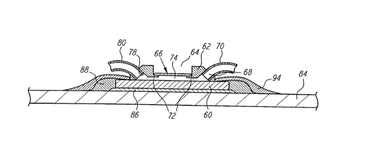
Fig. 6 shows a cross-sectional view of a fluidic
system in combination with a APEX like detection system.
Fig. 7 shows a plan view of the fluidic system of Fig. 6
in the larger environment of i~s inclusion on a printed
circuit board. Reference numbers will be utilized in
comment to the extent possible. A biochip 60, pre~erably
an APEX type chip as described above, is combined with a
fluidic system. In the preferred embodiment, the fluidic
system includes a flow cell 62. The flow cell 62 is
disposed adjacent and above the biochip 60, and preferably
in hermetic contact with the biochip 60. The flow cell 62
CA 02233238 1998-03-26
W O 97/12030 PCT~US96/14353
preferably includes an aperture 64 which permits optical
access to the biochip 60. A flow cell window 66 contacts
the flow cell 62 at the peripheral edges of the flow cell
window 66. The flow cell window may be a quartz, or other
suitable material chose in part for its transmission and
non-fluorescence properties. Advantageously, the flow
cell window 66 is chosen to have an index of re~raction
which substantially matches the index of refraction of the
sample solution. An inlet port 68 and an outlet port 70
are provided through the flow cell 62. A sample chamber
74 is de~ined by the ccmbination of the flow cell 62, the
flow cell window 66 and the biochip 60. In the preferred
embodiment, the sample chamber 74 has a volume from
approximately 5 to approximately 10 microliters. An input
tube 76 is preferably connected to the input port 68.
Optionally, the input tube 76 connects to a fluidic
interface port 78, such as formed by a female Luer taper
system. An output tube 80 is preferably connected to the
outlet port 70. The components of the fluidic system are
preferably formed from inert materials, e.g.,
tetrafluoroethylene, or other medical grade plastics. The
flow cell 62 and associated components may be formed
through any known technique, such as molding or machining.
The output tube 80 preferably provides a
communication path from the flow cell 62 to a reservoir
82. In the preferred embodiment, the reservoir 82 has a
minimum volume of approximately 1.2 ml. As shown, the
reservoir 82 is formed as a generally nonexpandable waste
tube. In this embodiment, the waste tube reservoir 82 is
filled by the fluid flow from the flow cell 62 through the
output tube 80. In another embodiment, the reservoir 82
may be an expandable structure, such as an expandable
mylar bag. The reservoir 82 may optionally operate under
vacuum, thereby providing additional force to cause the
sample to flow into the reservoir 82. Such a vacuum
structure may be formed such as through a vacutainer
CA 02233238 1998-03-26
W O 97/12030 PCT~US96/14353
24
The biochip 60 is preferably mounted on a printed
circuit board 84, such as a FR4 circuit board, via adhe-
sive 86. The adhesive 86 may be of any type conventional
used in the surface mount technology art, and may be
either conductive or nonconductive as desired. For
example, the adhesive 86 may be a thermally conductive
epoxy. Lead wires 88 connect from the biochip 60 to the
printed leads 90. Conventional techniques such as ball
bonding or wedge bonding using 0.001 inch AlSi or gold
wire may be used. The printed leads 90 are formed on the
printed circuit board through conventional techniques. As
shown in Fig. 7, the printed circuit board is formed in
the P~MCIA format, such that a 68 position electrical
contact 92 provides an lnterface between the printed leads
90 and the electronics connected to the electrical contact
92. Other conventional formats may be used.
Preferably, the lead wires 88 are potted or
encapsulated in a protective material 94, such as
nonconductive W resistant epoxy. Preferably, the
protective material 94 provides electrical insulation for
the lead wires 88, provides a moisture barrier for the
lead wires 88 and provides mechanical support ~or overall
device ruggedness. Overall rigidity of the printed
circuit board 84 and structures formed thereon is
generated by the optional frame 96.
With regard to the preferred mode of construction of
the structure of Figs. 6 and 7, the biochip 60 is
pre~erably attached via adhesive 86 to the printed circuit
board 84. Next, lead wires 88 are connected from the
biochip 60 to the printed leads 90. The lead wires 88 are
then encapsulated in the protective material 94, with the
central region of the biochip 60 disposed outward from the
adhesive 86 being kept clear. In the APEX device the
clear region is approximately 7. 5 mm2 ~ The flow cell 62 is
then directly bonded to the biochip 60. In the preferred
embodiment, the flow cell 62 may be formed of any material
compatible with the purposes and materials described, such
CA 02233238 1998-03-26
W O 97/12030 PCTAJS96/14353
as medical grade plastic. The biochip 60 may be formed,
such as from silicon. The flow cell 62 may then be
attached to the silicon of the biochip 60 by adhesives,
which would generally be relatively thin. The order of
affixing the flow cell 62 to the biochlp 60 and the
encapsulating of the lead wires in the 88 in the
protective material 94 may be reversed, namely the flow
cell 62 or components thereof may be affixed to the
biochip 60 prior to the addition of the protective
material 94.
Preferably, the biochip 60 is placed at the center of
rotational gyration of the structure of Fig. 7. In
certain embodiments, the biochip 60 includes a permeation
layer or other layer disposed at the surface of the
biochip 60. These materials are often spin-coated onto
the surface of the biochip 60. By placing the biochip 60
at the axis of rotation, the completed structure of Fig.
7, excluding the flow cell window 66, and optionally
excluding other components, e.g., the frame 96, the input
tube 76, the fluidic interface port 78, the output tube 80
and the reservoir 82, may be spun so as to add the
materials to the surface of the biochip 60. Since the
spin rates can often be relatively large, for example,
10,000 rpm for the spin-coating of certain polymers,
placing the biochip 60 at the center of rotation provides
for easier spin-coating. By forming the spun on
structures, such as a permeation layer and capture
sequences, a generic device of the type shown in Fig. 7
may be formed, and the suitable polymers and capture
sequences for an assay placed down as desired.
Additionally, by forming the assay related layers on the
biochip 60 after substantially all other structures have
been formed permits the precleaning of a manufactured
device prior to the addition of the biologically sensitive
materials, such as the permeation layer and the attachment
sequ-ences.
_
CA 02233238 1998-03-26
W O 97/12030 PCT/US96/lq353
26
Fig. 8 shows a complete system 100 for the automated
sample preparation and hybridization of prepared materi-
als. A sample 102, such as blood or other biological
materials are introduced into the system 100. Generally,
a sample addition port 104 is provided. Generally, the
sample addition port 104 is utilized when an overlying
biological containment structure is present such that the
sample 102 could not be directly placed into the system
without access via the port 104. Optionally, a
contAlnm-ont cover 106, such as glass or transparent
plastic, may be disposed over the system 100.
Sample preparation is performed in this system 100 by
the combination of the electronic cell sorter matrix
component 108 and DNA selector component 110 and restric-
tion fragment selector component 112. The selectorcomponent 112 may be further characteri~ed based upon its
intended use, such as a restriction fragment selector 112
or to isolate bacterial or viral nucleic acids from human
genomic or background DNA. The electronic cell sorter
matrix component 108 consists of underlying electrodes,
with permeation layers and an attachment layers. These
effectively form a matrix of locations ~or the attachment
of cells. Generally, the area for individual locations and
the complete matrix area are larger than the areas in an
analytical device component. Thus, the electronic cell
sorter matrix is scaled appropriately to accommodate
variation in the number of cells from different samples
and sample sizes. The attachment layers can be generally
selective for cells, or individual selective for different
types of cells. Optionally, groups or sets of locations
can be made selective for one type of cell. Cell
selectivity can be imparted by attaching specific
antibodies or cell adhesion factors to the attachment
layer. The matrix 108 operates by free field electrophore-
sis.
The crude DNA selector 110 and selector 112 serve tobind the crude DNA output from the electronic cell sorter
CA 02233238 1998-03-26
W O 97/12030 PCTrUS96tl~353
matrix 108 and permit selective cleavage of the deslred
DNA ~rom the bound material. The term crude is used
merely to denote a non-final stage in DNA isolation or
complexity reduction. The DNA is bound to the selec~or in
a region which is believed not to contain the desired DNA
material. The desired DNA materials are then severed from
the bound materials, such as by application o~ restriction
enzymes. In the case o~ infectious disease analysis, the
selector 112 would be designed to isolate bacterial or
viral nucleic acids ~rom human genomic or other background
DNA. The severed, unbound material is then physically
moved from the crude DNA selector 110 to the selector 112.
Preferably, electrophoretic transport is used to remove
the severed material. This process may be repeated by
binding the severed material to a selector, upon which a
restriction enzyme acts so as to cleave the unbound
portion which contains the desired DNA.
For example, human DNA contains approximately 100,000
genes. Of the total DNA material, a signi~icant portion
constitutes repeating sequences which do not contain the
desired DNA information. The DNA may be bound to a selec-
tor by these noninformation bearing repeating sequences.
The bound DNA may be severed ~rom the unbound DNA which is
believed to contain the desired DNA to be analyzed. This
process may then be repeated with yet more specific se-
quences causing binding of the material to the selector.
The output of the selector 112 is then supplied to
the APEX chip 114. Operations on the matrix 114 are
per~ormed as described in connection with Figs. 2A and 2B.
An electronic reagent dispenser system 116 may be
- provided to deliver reayents to the system 100.
Preferably, the reagents are delivered by electrophoretic
force if they are charged. Optionally, an electronic
waste disposal system 118 is lncluded within the system
100. The waste disposal system 118 attracts charged waste
particles to it and disposes of them by holding the
CA 02233238 1998-03-26
W O 97/12030 PCT/US96/143~3
28
charged entities on it. Another optional member of system
100 is the DNA fragment storage system 120. This fragment
storage system 120 serves to temporarily hold DNA
fragments for future analysis.
optionally, auxiliary electrodes 122 may be provided
in the system 100. The auxiliary electrodes 122 may
assist in the electrophoretic motion of materials
throughout the system 100. By providing selective acti-
vation of the auxiliary electrodes 122 along the long
axis, the motion of the materials may be aided or inhib-
ited.
In addition to the sample injection port 104, other
inputs and outputs beyond the system 100 may be optionally
included. For example, ~luid input and output ports 124
serve to provide additional addition of fluids to the
system 100. Further, electrical connections 126 are shown
disposed around the system 100 and serve to provide
electrical contact, such as to the driver board/computer
interface 138 (Fig. 9).
The system 100 may include some or all of the ~unc-
tions described above. For example, the combination of
sample preparation in the form of complexity reduction, as
performed by the DNA selector 110 and restriction fragment
selector 112 may be associated with the analytical matrix
114. However, any or all of the above described functions
may be combined as desired.
Fig. 9 shows a block diagram of the overall system
including the controller 130. The underlying electrodes
in an APEX device are made active by the application of a
controlled potential to the electrode or by the sourcing
of a controlled current through the electrode. Full
functionality is realized when the potential or current at
each electrode of the APEX device is independently
controlled. This is accomplished by an APEX controller
system.
The controller computer 130 interfaces with user
input/output devices, such as a display 132 and input
CA 02233238 1998-03-26
W O 97/12030 PCT~US96/14353
29
device 134. The display 132 may be any form of
conventional display such as a monitor or computer screen.
The input 134 may be any conventional user input device,
such as a keyboard, mouse, or touch-screen device. The
controller computer 130 is connected with the power supply
and waveform generator 136. The controller 130 sets the
power supply and waveform generator 136 to provide the
current or voltage output to the interface 138. In the
preferred embodiment, the power supply or waveform gen-
erator 136 is capable of providing precisely regulated andvoltage and current sourcing. The controller computer 80
provides control signals to the interface 138 via the
multifunction lnput/output board 140. The inter~ace 138
provides a simplified connection to the contacts for the
APEX system 142.
The interface preferably includes relays that permit
selective connection between the power supply and waveform
generator 136 to the specific electrodes of the APEX
system 142. In one embodiment, the interface 138 comprises
a plurality of relays which connect the power supply and
waveform generator 136 to the APEX system 142 electrodes.
The connections permit the selection or non-selection of
a path between the power supply and waveform generator 136
to the APEX system 142 electrodes. Additionally, another
relay permits selecting the polarity of the voltages
supplied to the APEX system 142 electrodes. Optionally, if
multiple source levels are available, such as from a
multiple output power supply 136, the specific level to be
connected to an APEX system 142 electrode may be set
independently of those for the other electrodes.
Thus, as described in connection with Fig. 2A, by
placing certain electrodes (e.g., 12B and 12C) at a nega-
tive, but lesser potential than electrode 12D, the attach-
ment region 16B and 16C would be protected by the local
force ~ield.
The interface 138 may serve to select the desired
voltage for the individual electrodes in the APEX system
CA 02233238 l998-03-26
W O 97/12030 PCT~US96/14353
142. Alternatively, such a different voltage arrangement
may be achieved through use of a voltage divider.
In the pre~erred embodiment, the controller computer
130 iS a Macintosh Quadra 950. National Instruments
Corporation LabVIEW software is used to provide a software
interface ~or a user to program the devices connected to
the APEX and to collect and process data from an assay.
National Instruments NuBus boards are used to provide the
hardware interface from the Quadra 950 computer 130 to the
power supply devices 136 that source potentials and cur-
rents and that measure the actual currents and potentials
and the results o~ the assay.
The user controls the assay through a Virtual Instru-
ment created with the LabVIEW software. The virtual
instrument provides a user ~riendly graphical representa-
tion o~ the controls that the user may exercise, and of
some of the results of applying these controls to the APEX
device to perform an assay. The user interfaces with the
Virtual Instrument through the keyboard and mouse (collec-
tively, input 134) of the Quadra 950 computer 130. The
Virtual Instrument provides software interfaces to a
National Instruments NB-MIO-16XL multipurpose input/output
140 and to a National Instruments DMA2800 board that are
connected to the NuBus data bus of the Quadra 950.
The multipurpose I/O board is able to provide digital
and/or analog signals to external devices to implement the
programmed sequence specified by the user through the
Virtual Instrument. The MIO board is also able to
digitize and store in the Quadra 950, under control o~ the
Virtual Instrument, signals generated by the devices
connected to the APEX. The DMA2800 provides the ability
to store rapidly the data acquired by the MIO board
through Direct Memory Access, bypassing the Quadra 950
CPU. The DMA 2800 also provides a GPIB (IEEE 488) inter-
face for control of external devices that adhere to the
IEEE 488 communication and data transfer standard, which
includes most modern instruments.
CA 02233238 1998-03-26
W O 97/12030 PCT~US96/14353
In this pre~erred embodiment o~ the controller, two
external devices are used to source the potentials or
currents to the APEX. A Keithley 236 Source/Measure Unit
power supply 86 provides adequate stability and
flexibility as a source of precisely regulated potential
or current. The SMU 236 either applies a potential and
measures the resultant current or provides a source of
current and measures the resultant potential. This device
is programmed from the Virtual Instrument under GPIB
control through the DMA2800 board to control the current
or potential levels and time dependence, and to measure
and store the actual potentials and currents that are
sourced to the APEX.
The sourced currents or potentials are applied to the
APEX through an array of relays in interference 138 that
provide independent switching of each electrode between no
connection, connection to positive source and connection
to negative source. The preferred embodiment also
provides for more than one Source/Measure supply to be
utilized to provide different levels of positive and
negative potential or current to different electrodes.
The array of relays is provided by a National Instruments
SCXI Chassis with nine 16-channel, Class 3 Relay Modules
connected in the chassis, providing a total of 144 relays.
Two relays are used per electrode to provide for electrode
disconnected or electrode connected to either positive or
negative source. In the preferred embodiment, a bundle of
cables connects these relays to the APEX device through a
Cerprobe Probe Card that provides mechanical contact of
probes to the bond pads o~ the APEX device.
The controller computer 130 optionally controls the
illumination source 144 for excitation of fluorescence to
detect DNA hybridization. In the preferred embodiment,
the illumination source 144 is a laser which outputs
radiation at an appropriate wavelength to excite fluo-
rescent markers included within the APEX system 142.
CA 02233238 l998-03-26
W O 97/12030 PCT~US96/1~353
32
The output of the APEX system 142 i9 passed through
observation path 146 to the detector 148. The observation
path 146 may be a physical connection, such as through a
fiber optic, or may comprise an optical path such as
through a microscope. Optical filters may be utilized in
the observation path to reduce illumination of the
detector at wavelengths not corresponding to the emission
spectra of the fluorescent markers in the APEX system 142.
Additionally, notch filters may be utilized as necessary
to reduce illumination of the detector 148 at the
excitation wavelength of the laser illumination source
144. The detector 148 may optionally form an image of the
APEX system 142, such as through the use of a cooled CCD
camera. In addition to, or as an alterative to, forming an
optical image, the emitted fluorescence radiation from the
APEX system 142 may be detected by conventional means such
as photodiodes or photomultiplier tubes. The output of
the detector 148 iS provided to the data
processing/analysis system 150. This system monitors the
level of detected probe material in the APEX system 142.
Optionally, an expert system may be utilized in the
analysis system 150.
In the preferred embodiment, a Data Translation Frame
Grabber board is interfaced to the Quadra 950 NuBus, to
2 5 provide capture to memory of images recorded by video
cameras such as the Optronics cooled color CCD camera used
in the preferred embodiment. This CCD camera observes the
APEX device through a microscope with appropriate filters
to provide visualization of fluorescence on the APEX
array.
Alternate systems may implement all the functionality
of the controller as described, but may use custom devices
incorporated into printed circuit boards and custom soft-
ware to control the board with a similar user-friendly
interface for programming the device. These alternate
systems may also incorporate the switching elements of the
CA 02233238 1998-03-26
W O 97/12030 PCT/US96/14353
33
array of relays into a semiconductor device underlying the
active, programmable matrix system.
The permeation layer (e.g., layer 14 of Fig. 2) may
be formed from materials such as, but not exclusive to,
membranes, metal oxides (e.g., aluminum oxide), carbon
chain polymers, carbon-silicon chain polymers, carbon-
phosphorous chain polymers, carbon-nitrogen chain poly-
mers, silicon chain polymers, polymer alloys, layered
polymer composites, interpenetrating polymer materials,
ceramics, controlled porosity glass, materials formed as
sol-gels, materials formed as aero-gels, materials ~ormed
as hydro-gels, porous graphite, clays or zeolites.
Permeation layers separate the binding entities from
the surface of the electrode. Micro-locations have been
created using microlithographic and micro-machining tech-
niques. The permeation layer may be disposed within a
well (see, e.g., Fig. 2A) or may not be recessed and
simply be coated with a permeation layer covering the
electrodes. Either of these arrangements may be formed by
spin coating of the permeation layer. Chemical
modification of the surface of the micro-locations and of
polymer layers over the micro-locations have been used to
create specialized attachment sites for surface func-
tionality.
Mesh type permeation layers involve random
arrangements of polymeric molecules that form mesh like
structures having an average pore size determined by the
extent of cross-linking. We have demonstrated the
formaticn of mesh type permeation layers using several
polymerizable formulations containing acrylamide as a
monomer. We have used triethylene glycol diacrylate,
tetraethylene glycol diacrylate and N, N'-Methylene-bis-
acrylamide as cross-linking agents. Poly-l-lysine with
molecular weights of 330 kilodaltons and 25 kilodaltons
was mixed into the acrylamide/copolymer formulation to
provide a means for attaching specialized functionality to
the surface of the permeation layer. The mixture was cast
CA 02233238 1998-03-26
W O 97/12030 PCTrUS96114353
onto the surface of the micro-location. It was then
photopolymerized by ultraviolet light. In some cases,
AuC14 was added as a photoinitiator. The polymer
formulations were cast from water and the nona~ueous
solvents, methanol, tetrahydrofuran, acetonitrile,
acetone, and mixtures of these solvents.
DNA capture probe was attached to the surface of the
permeation layer by a Schiff base reaction between an
oxidized ribonucleoside attached to the DNA capture probe
and the primary amine of the poly-l-lysine. This provides
evidence of covalent attachment of special functionality
to the surface of the permeation layer.
An oxidized DNA capture probe was brought to a
surface micro-location by electrophoretic transport. The
capture probe was labeled with a fluorescent marker. This
demonstrates the ability to address a micro-location by
electrophoretic transport.
An oxidized capture probe with a fluorescent marker
attached was attracted to the surface of the permeation
layer at a micro-location by electrophoretic transport.
The permeation layer was removed from the micro-location
by mechanical means. No evidence of the presence of the
fluorescently labeled capture probe was observed. This
demonstrates the ability of the permeation layer to
protect the DNA from the electrode surface.
The maximum DC current density that was attained at
a gold micro-location, which was not modified with a
permeation layer, before bubbles due to water hydrolysis
appeared was 8 milliampheres/cm2. The maximum DC current
density that was attained at a gold micro-location, which
was modified by an acrylamide-based permeation layer,
before bubbles due to water hydroly,sis appear was 40
milliampheres/cm2. This demonstrates the ability of the
permeation layer to raise the maximum accessible current
density before bubbles form due to water hydrolysis.
An ionomer sandwich permeation layer is formed from
one or more lamina of polyelectrolytes. The
CA 02233238 1998-03-26
W O 97/12030 PCTAJS96/14353
polyelectrolyte layers may have the same charge, different
charge, or may be charge mosaic structures
A two layer ionomer sandwich layer was formed from a
base layer of a perfluorinated sulfonic acid polyelectro-
lyte (Nafion) and an upper layer of poly-l-lysine. The
base Nafion layer was cast onto a micro-location and
allowed to dry. This base layer was then exposed to a 1%
by weight aqueous solution of poly-l-lysine. The cationic
lysine-based polymer adsorbed strongly to the anionic
Nafion base layer. The poly-l-lysine layer allowed the
attachment of an oxidized DNA capture probe to the surface
of the permeation layer by a Schiff base reaction. The
Nafion base layer is anionic and is permselective toward
negative ions such as DNA.
Fig. 10 shows examples of the graphical user inter-
face. Window 160 shows an overall view of the display.
Identification information 162 is provided. The various
pads of the active, programmable matrix system are identi-
fied in a rectangular coordinate system. The displays 164
each show the electrical parameter, such as current or
voltage for particular pads. Box 164A shows the current
as a function of time for a pad, (3,4), wherein the
current varies as a function of time, changing directions
during the course of the application. Box 164B shows a
pad, (3,5), having no applied current during the time
shown. Box 164C shows a time varying current for pad
(4,4), wherein that current is delayed with respect to
time relative to the pad (3,4) reported in Box 164A. Box
164D shows a pad, (4,5), with no applied current as a
function of time. Box 164E shows a pad, (1,1), for which
- the voltage has a constant, negative DC value. Box 164F
shows the voltage as a function of time for a pad, (3,4)
having a more negative DC value. In all cases, the boxes
show the programmed current or voltage as a dotted line,
and the measured current or voltage as a solid line.
In addition to the preferred embodiment of the inven-
tion and the alternatives described above, several more
CA 02233238 1998-03-26
WO 97/12030 PCT~US96/14353
3~
alternatives are possible. For example, the electric
field that gives rise to ion migration may be modulated in
time as long as a DC bias voltage or current is applied
simultaneously. The use of an AC signal superimposed on
a DC bias voltage or current can achieve three things, 1)
minimize the background due to nonspecifically bound DNA,
2) provide a means of electronic stringency control where
the control variable is the frequency of the alternating
current or voltage, 3) provide a means of aligning DNA
molecules spatially.
Many alternatives to the detection of hybridized DNA
by fluorescence exist. Most of the alternative techniques
also involve modification of capture or target or reporter
DNA probes with reporter groups that produce a detectable
signal. A few of these techniques based on purely
physical measurements do not require reporter groups.
These alternative techniques are catalogued as follows:
(1) Linear Optical Methods including fluorescence, time
modulated fluorescence, fluorescence quenching modulation,
polarization selective fluorescence, absorption, specular
reflectance, changes in index of refraction, ellipsometry,
surface plasmon resonance detection, chemiluminescence,
speckle interferometry and magneto-optic Kerr effect; (2)
Nonlinear Optical Methods including second harmonic
generation, third harmonic generation, parametric mixing,
optical heterodyne detection, phase conjugation, soliton
damping and optical Kerr effect; (3) Methods Based on
Thermal Effects lncluding differential scanning
calorimetry, multifrequency differential scanning
calorimetry, and differential thermal analysis; (4)
Methods Based on Mass Changes including crystal
microbalances, cantilever microbalances, surface acoustic
waves and surface Love waves; (5) Electrochemical
Methods including amperometry, coulometry, voltammetry,
electrochemiluminescence, charge transfer in donor-
acceptor complexes and surface impedance spectroscopy; and
(6) Radioactivity Detection Methods using labeled groups.
-
CA 02233238 1998-03-26
W O 97/12030 PCTAJS96/14353
Fig. 11 shows a cross-sectional view of an lmproved
detection system. A sample 170 includes a region of
interest 172. The region of interest 172 may include
multiple areas on the sample 170. Any o~ the various
excitation sources 174 and detectors 176 as are
conventionally used in fluormetric systems may be utilized
with this invention.
Delivery of energy from the excitation source 174 to
the region of interest 172 is pre~erably accomplished via
a excitation fiber 178. The excitation fiber 178 is
preferably fiber optic light guide. The excitation fiber
178 has an input end 180 and an output end 182. The
output end 182 may be formed in a manner as known to those
skilled in the art so as to provide focused projection of
the energy ~rom the excitation source 174. Optional fiber
launch system optics 184 receive the output o~ the
excitation source 174 and provide the radiation to the
input end 180 of the excitation fiber 178.
Radiation emanating from the region of interest 172
(shown as dashed lines between the region of interest 172
and detector 176) is passed through light guide 186. The
light guide 186 preferably comprises a liquid light guide
portion 188. The liquid light guide 188 is surrounded by
a housing 190, which serves to contain the liquid light
guide 188. A proximal lens 192 is disposed within the
housing 190 at that portion of the light guide 186 which
is disposed towards the region of interest 172. A distal
end 194 is disposed within the housing 190 at the end of
the light guide 186 disposed towards the detector 176.
In the preferred embodiment, the excitation fiber 178
is formed coaxially in the light guide 186. Preferably,
the output end 182 of the excitation fiber 178 is disposed
through aperture 196 in the proximal lens 192. In this
manner, the radiation from the excitation source 174 may
be supplied through the excitation fiber 178 and delivered
to the region o~ interest 172 without passing through the
optical components of the proximal lens 192.
CA 02233238 l998-03-26
W O 97/12030 PCT~US96/14353
38
Alternatively, the output end 182 of the excitation fiber
178 may be disposed within the liquid light guide 188 such
that the radiation of the excitation source 174 passes
through the optical component of the distal lens 194
before being supplied to the region of interest 172. The
use of the excitation fiber 178, such as when a fiber
optic, permits a degree of mechanical decoupling between
the excitation source 174 and the sample 170. For
example, the excitation source 174 and the detector 176
may be fixed in place while the light guide 186 and
excitation fiber 178 are moved over the sample 170.
Pre:Eerably, the excitation :Eiber 178 includes an axially
region 198 which is disposed along the axis of rotation of
the light guide 186. This concentric axial alignment of
the optical paths of the axial region 198 of the
excitation fiber 178 and the light guide 186 provide for
alignment to the detector 176. The liquid light guide 188
advantageously provides for more complete transference of
the energy from the region of interest 172 to the detector
176. Alternatively, fiber bundles may be utilized in the
light guide 186, though the liquid light guide 188
provides more complete coverage of the output from the
proximal lens 192.
The APEX device as described previously has been
utilized in novel ways resulting in method which improve
the analytical or diagnostic capabilities of the device.
It has been surprisingly discovered that the fluorescent
signal is perturbed during the electronic denaturation of
DNA hybrids. This method has particular application to
DNA hybridization and single-base mismatch analysis.
Specifically, during electronic denaturation, also known
as stringency control, a rise or spike in the fluorescence
intensity has been observed just prior to the
dehybridization of the fluorescent labelled probes from
capture sequences attached to the APEX chip pad.
Figs. 12A and 12B show the results of electronic
denaturization experiments run on an APEX chip having 25
CA 02233238 1998-03-26
W O 97/12030 PCT~US96/14353
39
test microlocations with 80 micron diameter utilizing
platinum electrodes. For this use, the chip was overlaid
with a 1 micron thick avidin/agarose permeation layer,
Two 5'-labeled bodipy Texas Red (Ex 590 nm, EM 630 nm)
target probes were used in the experiments. The probe of
Fig. 12A was a 20 mer (5'-BYTR-AAATTTTAATATATAAT-3')
containing 100% AT, with a melting temperature (Tm) of
33~C. The probe of Fig. 12B was a 19 mer (5'BYTR-
CCACGTAGA~CTGCTCATC-3') containing 53% GC, with a melting
temperature (Tm) of 54~C. (Melting temperature or Tm
refers to the temperature at which the dehybridization
process is 50% complete). The appropriate complementary
biotinylated capture sequences were attached to the
avidin/agarose permeation layer over several of the test
pads (on the same chip). The capture probe density was
_108 probes per pad. The fluorescent labeled target
probes, at a concentration of ~1.0 ~M in 50 mM sodium
phosphate (pH 7.0), 500 mM NaCl were first hybridized to
the attachment probes on the 5580 chips. The chips were
then thoroughly washed with 20 mM NaPO4 (pH 7.0).
Electronic denaturation was then carried out by
biasing the test pad negative, and increasing the power to
the test pad from ~10~l microwatts (~W) to ~2 x lOZ
microwatts (~W) over a 90 second time period. Three pads
were tested for each of the target probes. The relative
change in fluorescent intensity was plotted as a function
of the increasing power. In general, the electrophoretic
force or power necessary to de-hybridize a probe from its
complementary sequence correlates with the binding energy
or Tm (melting temperature) for the DNA duplex. In above
experiments the overall power level (~W) necessary to de-
hybridize the 19-mer probe with 53% GC probe (Tm of 54~C)
was higher than for the 20-mer probe with 100% AT (Tm of
33~C), that is, the equivalent electronic melting point
(Em) at which dehybridization is 50% complete is higher
for the 53% GC probe. Also, the fluorescent perturbation
(Figs. 12A and 12B, circled region) for the 10-mer probe
CA 02233238 1998-03-26
W O 97/12030 PCT~US96/14353
with 53% GC is observed to be significantly dlfferent from
that associated with the 100% AT probe.
Figs. 13A and 13B show the results of denaturation
experiments run on the APEX chip having 25 test
microlocations with 20 micron deep wells to the underlying
platinum electrodes. The well structures on the chip were
filled with avidin/agarose composite, forming a 20 micron
deep permeation layer. The same fluorescent target
probes, capture probes and protocols were used in the deep
well experiments as in the operation of the device
resulting in the information of Figs. 12A and 12B. As in
the first experiments, the overall power (~W) necessary to
de-hybridize the 19-mer probe with 53% GC (Tm of 54~C), is
higher than for the 20-mer probe with 100% AT (Tm of
33~C). Also, the slope for the 100% AT probe is much
shallower, then for the 53% GC probe. The fluorescent
perturbation/spike phenomena is very pronounced for the
19-mer probe with 53% GC in the deep well experiments.
The fluorescent perturbation phenomena correlates
well with the se~uence specificity of the dehybridization
process. The power level (~w) value, amplitude and slope
of the fluorescent spike are useful for many aspects of
hybridization analysis including single base mismatch
analysis. The fluorescent perturbation (Fp) value, namely
those values associated with the fluorescence
perturbation, e.g., onset value, peak height and slope,
combined with the electronic melting (Em) values, namely,
the half-height value of fluorescence, provide
significantly higher reliability and additional certainty
to hybridization match/mis-match analysis. By combining
two or more analytical measurements, a more effective and
precise determination may be made.
In the above experiments, the target probes were
labeled with a Bodipy Texas Red fluorophore in their 5'
~erminal positions. While Bodipy TR is not a particularly
environmentally sensitive fluorophore it nevertheless
showed pronounced effects during electronic denaturation.
CA 02233238 l998-03-26
W O 97/12030 PCT~US96/14353
41
More environmentally sensitive fluorophores may be used to
obtain larger perturbations in their ~luorescent
properties during electronic de-hybridization.
The placement of a sensitive fluorescent label in
optimal proximity to the initial denaturation site is
preferred. By associating the fluorescent label in
proximity to the denaturation site, as opposed to
labelling at the end of the target or probe, increased
specificity and enhanced effect may result. AS shown in
Fig. 14A and 15A, an intercalcating fluorophore 200 may be
disposed between a reporter probe 202 and target DNA 204.
Fig. 14A shows the condition in which the reporter probe
202 is mismatched from the target DNA 204 by a mismatched
base 205. In each of Figs. 14A and 15A, the capture probe
15 208 serves to capture the target DNA 204, with the pad 210
providing the electrophoretic action. Preferably, the
intercalcating fluorphore 200 would be placed next to the
single base mismatch site 206 (Fig. 14A). The
intercalcating type ~luorescent label could be, for
example, ethidium bromide or acridine, or any other known
fluorescent labels consistent with the objects of this
device and its use.
Fig. 14B and 15B show the condition of the reporter
probe 202, the target DNA 204 and the mismatch base site
206 a:Eter the application of a pulse at the ~luorescent
perturbation value via the pad 210. The change from
intercalated to the non-intercalated environment would
produce a major change in fluorescent signal intensity of
the label.
Furthermore, the use of a mis-match site directed
~luorophor label does not require that the hybrid be
completely denatured during the process. As shown in Fig.
14C and Fig. 15C, an analysis procedure is preferred in
which an appropriate pulsed "Fp" power level is applied
which causes a mis-matched hybridization site to partially
de-nature and re-nature relative to a matched
hybridization site. The procedure results in an
CA 02233238 1998-03-26
W O 97/12030 PCTAJS96tl4353
42
oscillating fluorescent signal being observed for mis-
match hybrid site, while the fluorescent signal for the
matched hybrid site rem~1nq unchanged. Figs. 14C and 15C
shows the relative fluorescent intensity as a function of
varied applied power. This procedure provides a highly
specific and discriminating method for single base mis-
match analysis. Additional advantages include: (1)
Longer probes (~ 20-mer) than those used in conventional
hybridization procedures can be used in this process, (2)
Probe specificity is more determined by placement of the
fluorescent label (particularly for single base mis-
matches), and (3) as the procedure does not require
complete denaturation of the hybrid structures, each
sample can be analyzed repetitively for providing a higher
statistical significant data, such as through standard
averaging techniques.
The electronic stringency device disclosed herein may
be advantageously used for DNA fingerprinting and
analysis. An electronically addressable array measures
DNA fragment sizes by determining the different electronic
force necessary to dehybrize the fragment of varying
lengths from capture probe sequences. As shown in Fig.
16A-D, three test sites 210 are shown labelled test sites
A, B and C. This number of test sites may be greatly
increased in an actual device, but three are shown for
demonstration of the principle and technique. Capture
probes 212 would be attached to the test sites 210 through
the techniques described above. Fragments of a given,
though likely unknown, first length 214 would be
hybridized with the capture probe 212 at test site C 210.
A second fragment 216 having presumably a different length
than fragment 214 is hybridized to capture probe 212 at
test site B 210. Similarly, a fragment 218 having a
presumably different length than fragments 214, 216 is
hybridized to capture probe 212 at test site A 210.
The test sites 210 are then subject to reverse
potential at increasing current levels. The fluorescence
CA 02233238 1998-03-26
W O 97/12030 PCT~US96/14353
~rom the test sites 210 is monitored. As the reverse
potential is increased, indications of dehybridization are
detected, such as by observing the peak as described in
connection with Figs. 12A, 12B, 13A and 13B, or by
complete dehybridization. In the preferred embodiment,
the complete dehybridization o~ the ~ragments 214, 216 and
218 are detected from the capture probes 212. Since the
varying length fragments 214, 216 and 218 have di~erent
lengths, they will have di~erent amounts of net charge.
Thus, as the potential at test sites 210 is increased,
those fragments 214, 216 and 218 having larger net charge
will be subject to larger force, and accordingly, be
removed from the test site 210 at a lower potential. Fig.
16B shows the condition in which the test site C 210 has
reached or exceed a reverse potential which caused the
dehybridization of the fragment 214 from the capture probe
212. Next, as shown in Fig. 16C, when the reverse
potential at test site 210 reaches that level at which the
fragment 216 is subject to sufficient force to dehybridize
from capture sequence 212, the ~ragment 216 separates ~rom
test site B 210. Finally, as the reverse potential is
increased even further, the shortest ~ragment 218 is
removed from the capture sequence 212 at test site A 210.
In this way, the electric potential or current required to
resolve different sized fragments from each test site is
determined and correlated with the ~ragment size.
Although the foregoing invention has been described
in some detail by way of illustration and example ~or
purposes of clarity and understanding, it will be readily
apparent to those of ordinary skill in the art in light of
the teachings of this invention that certain changes and
modi~ications may be made thereto without departing from
the spirit or scope of the appended claims.