Note: Descriptions are shown in the official language in which they were submitted.
CA 02233317 1998-03-27
W O 97/12401 PCT~US96/15717-
A SILICIDE AGGLOMERATION FUSE DEVICE
RELATED APPLICATION
This application is related to U.S. Patent Application Serial No.
, entitled, "A Low Voltage, High Gain Fuse Sensing Circuit and
Method", filed September 29, 199~ (Attorney's Docket No.
42390 . P3 1 81 ) .
FIELD OF THE INVENTION
The invention relates to the field of integrated circuit devices and
more particularly, to fusible link devices in semiconductor integrated
ci rcuits.
BACKGROUND OF THE INVENTION
In integrated circuits including CMOS integrated circuits, it is often
desirable to be able to permanently store information, or to form
permanent connections on the integrated circuit after it is manufactured.
Fuses or devices forming fusible links are frequently used for this
purpose. Fuses can be used to program redundant elements to replace
identical defective elements, for example. Fuses can also be used to
store die identi~ication or other such information, or to adjust the speed
of a circuit by adjusting the resistance of the current path.
In some cases, electrically erasable programmable read only
memory (EEPROM) devices are used to perform the discretionary
connection function of a fuse device. Semiconductor process
technologies continue to provide for smaller device geometries and
operate at lower voltages. As the device geometries are reduced, so is
the thi~knes~f t~e g~e ~xi~e layer. i-i_PR(3i~/1 fuse devices require a
relatively thick gate oxide to prevent high leakage currents and sustain a
charge on the floating node. Thus, EEPROM fuse devices are not viable
for use on many of the latest semiconductor process technologies.
Other hse devices require an extra semiconductor processing
step to form or program the discretionary connections. For example,
one type of fuse device is "programmed" using a laser to open a link
CA 02233317 1998-03-27
W O 97/12401 P ~ AUS96/1571
after the semiconductor device is processed and passivated. This type
of fuse device not only requires an extra processing step to program or
"blow" the fuse devices where desired, but also requires precise
alignment of the laser on the fuse device to avoid destroying
neighboring devices. This and other similar approaches can result in
damage to the device passivation layer, and thus, lead to reliability
concerns. In some approaches, the passivation layer must actually be
removed before programming the fuse device to provide space for the
fuse material when the connection is destroyed. In other approaches,
where the passivation layer is not intentionally removed, the process of
blowing the fuse can cause a hole in the passivation layer when the
fuse material is displaced.
Another type of fuse device, referred to as an "oxide antifuse"
device, is programmed using high voltages compared to the circuit's
normal operating voltage supply. Therefore, the peripheral circuitry for
these devices, generally requires higher junction breakdown voltages
than thoss normaliy available on the integrated circuit. This is an issue
for newer process technologies, and those in development, for the same
reasons described above in reference to EEPROM fuse devices. The
reduced gate oxide thicknesses require higher well doping which
results in lower- junction breakdown voltages, and thus, oxide antifuse
devices may also not be viable for use with many of the latest process
technologies.
The invention provides a small fuse device which can be
manufactured without additional processing steps, and which can be
reliably used with today's lower voltage, thinner gate oxide process
technologies. Further, the fuse device of the invention can be
programmed using relatively low voltages without damage to overlying
dielectric layers.
SUMMARY OF THE INVENTION
A fusible link device disposed on a semiconductor substrate for
providing discretionary electrical connections is described. The fusible
link device of t~le invention has a first un-programmed resistance and
CA 02233317 1998-03-27
W O 97/12401 PCTAJS96/15717
includes a polysilicon layer and a silicide layer. The silicide layer is
formed on the polysilicon layer, and agglomerates to form an electrical
discontinuity in response to a predetermined programming potential
being applied across the silicide layer, such that the resistance of the
fusible link device can be selectively increased to a second
programmed resistance.
BRIEF DESCRIPTION OF THE DRAWINGS
Figure ~A illustrates a side view of the fusible link device of one
embodiment of the invention.
Figure 1 B illustrates a top view of the fusible link device of one
embodiment of the invention.
Figure 2A illustrates a side view of the fusible link device of one
embodiment of the invention after programming.
Figure 2B illustrates a side view of the fusible link device of an
alternate embodiment of the invention after programming.
Figure 3 illustrates the programming circuit and fusible link
device of one embodiment of the invention.
Figure ~ illustrates the sensing circuit and fusible link devices of
one embodiment of the invention.
Figure ~ illustrates an arrangement of the redundant fuse
devices of one embodiment of the invention.
Figure 6 illustrates the fuse programming and sensing method
of one embodiment of the invention.
DETAILED DESCRIPTION
CA 02233317 1998-03-27
W ~ 97/12401 PCTAUS96/15717
A silicide agglomeration fuse device for forming discretionary
connections is disclosed. In the following description, numerous
specific details are set forth, such as particular materials, dimensions,
numbers of contacts, programming and sensing voltages and currents,
in order to provide a thorough understanding of the invention. However,
it will be appreciated by one of ordinary skill in the art that the invention
may be practiced without these specific details. In other instances, well-
known structures, circuit blocks, interfaces, and architectural functions
have not been described in detail in order to avoid obscuring the
invention.
Overview of the Fuse Device of One Embodiment of the
Invention
Figure 1A illustrates a side view of one embodiment of the silicide
agglomeration fuse device 100 of the invention. The fuse device 100 is
disposed on a semiconductor substrate 107, and is usually part of a
larger integrated circuit device. In one embodiment, the polysilicon
layer 105 is doped p-type. Other embodiments may include other types
of doping including n-type as well as the formation of p-n junctions in the
polysilicon layer 105. An example of a fuse device 200 including such a
polysilicon layer, is described below in reference to Figure 2B. An oxide
layer 106, has ~ thickness 112 of about 3000 - 4000 = in one
embodiment, and is formed between the fuse device 100 and the
substrate 107.
The fuse device 100 includes a silicide layer 104 disposed on a
polysilicon layer 105. In one embodiment, the silicide layer 104 and the
polysilicon layer 104 of the fuse device 100 are formed by the same
processing steps used to produce the polysilicon and silicide gate
layers of other devices on the integrated circuit device. In this manner,
no additional processing steps are required to manufacture the fuse
device 1 00.
The polysilicon layer 105 is formed on the oxide layer 106 and
has a thickness 114 of 2500 z in one embodiment. The sheet
resistance of tt,e polysilicon layer 105 is greater than 500 ohm/sq.,
CA 02233317 1998-03-27
W O 97/12401 PCTAUS96/1571
about 1000 ohm/sq. in one embodiment, but may be more or less in
other embodiments of the invention. In one embodiment, the silicide
layer 104 is a titanium silicide (TiSi2) film, although other silicides, such
as tungsten, tantalum or platinum silicides, may also be used in
accordance with the invention. The silicide layer 104, has a thickness
110 of about 225-2~0 - in one embodiment, but may be thicker or
thinner in other embodiments. The sheet resistance of the silicide layer
104 depends on its exact composition, but is about 1-10 ohm/sq, in one
embodiment.
The fuse device 100 also includes contacts 101 at either end of
the fuse device 100. The contacts 101 are coupled to the silicide layer
104 to provide an electrical connection between the fuse device and an
external device or other components in the same integrated circuit
device. In one embodiment, contacts 101 are coupled to metal
interconnect lines (not shown) such that the fuse device 100 may be
accessed for programming~ g ~ oth2r U~B~. -Th~ cointact~ 1 û1 arz
tungsten plugs in one embodiment, but may be formed of other
materials. In alternate embodiments, metal interconnect lines of the
integrated circuit in which the fuse device 100 is formed, are coupled
directly to the silicide layer 104 to provide the same functionality.
The fuse device 100 of the invention is described in more detail
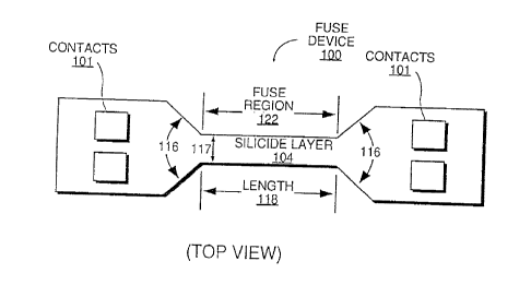
with reference ;:o Figure 1 B, which shows a top view of the device 100 of
one embodiment. The fuse device 100 includes a fuse region 122, also
referred to herein as a fuse element, between two contact regions 120.
The fuse device 100 may also include tapered transitional regions 116
between either end of the fuse region 122 and the respective contact
region 120. In this embodiment, each transitional region forms
app~im~t~ ~ 45Oo angie between the respective contact region 120
and the fuse region 122 such that current flowing between the contacts
is concentrated in the fuse region 122 during programming. The
geometries of the transitional re~ions 1 16 can contribute to lowering the
required programming voltage of the fuse device 100 as described in
more detail below. In alternate embodiments, the contact regions 120
are round, square or rectangular in shape. Also in alternate
CA 02233317 1998-03-27
-
W O 97/12401 PCT~US96/1~71
embodiments, ~he fuse device 100 may not include a transitional region
between the contact regions 120 and the fuse region 122.
The size of the fuse region 122 can vary with different processing
technologies, space considerations, and other fuse requirements. In
one embodiment, the width 117 of the fuse region from the top view
shown in Figure 1 B is close to the lower limit of the process technology
used to form the fuse device 100, about .22 microns in one example,
and the length 118 is between four to twenty-five times the width 117 of
the fuse region 122. In a particular embodiment, the length 118 is about
10 times the width 117, but may be larger or smaller in other
embodiments.
The con~act region 120 is as small as possible in one
embodiment, ~hile still providing the minimum area required by
contacts 101 based on their size, composition, and the programming
current or voltage required to program the fuse device 100. The number
of contacts 101 on the fuse device 100 may vary. Although two contacts
101 are shown at either end of the fuse device 100 in Figure 1 B, a larger
or smaller num~er of contacts may also be used in accordance with the
invention. In one embodiment, each of the contact regions 120 on either
end of the fuse device 100 includes nine contacts 101. Multiple contacts
101 operating in parallel may be used to ensure that the required
programming current flows through the fuse device 100 without
overheating the contacts 101.
In operation, the fuse device 100 has a first resistance before it is
programmed or ~'blown~, and a significantly higher second resistance
after programn:ing. Before the fuse device 100 is programmed, its
resistance is determined by the resistance of the silicide layer 104.
During programming, a discontinuity is formed in the silicide layer 104.
The resistance of the fuse device thus increases significantly based on
the ratio of the resistance of the polysilicon layer 10~ to that of the
silicide layer 1û4.
The effects of programming the fuse device 100 are described in
more detail in reference to Figures 2A and 2B. Figure 2A illustrates a
side view of the fuse device 100 of the invention after programming. A
CA 02233317 1998-03-27
W O 97/12401 PCTAUS96/15717-
programming potential applied across contacts 101 causes current to
flow from one end of the fuse device 100 to the other, through the
silicide film layer 104. The current causes the silicide layer 104 to heat
up, and the silicide itself to agglomerate as indicated by silicide
agglomeration region 204. A discontinuity 206 is thus formed in the
silicide layer 104 capping the polysilicon layer 105.
Because the silicide layer 104 has a much lower resistance than
the polysilicon layer 105, the resistance of the fuse device 100
increases accordingly. Using the sample sheet resistances provided
above (1 -10 ohms/sq for the silicide layer 104 and >500 ohms/sq for the
polysilicon layer), the resistance of the fuse device increases at least ten
times after programming. In some embodiments, such as the
embodiment described with reference to Figure 2B, the increase in
resistance is much greater. This change in resistance is then detected
by a sensing circuit to determine whether the fuse device 100 has been
programmed. The programming and sensing circuits of the invention
are discussed in more detail below with reference to Figures 3-6.
Figure 2B illustrates a side view of a programmed fuse device
200 in accordance with another embodiment of the invention. The fuse
device 200 includes contacts 201, a silicide layer 234, an oxide layer
236 and a substrate 237 which are similar in composition, placement
and functionality to identically named components of the fuse device
100 described above. The polysilicon layer 205 of the fuse device 200,
however, differs from the polysilicon layer 105 of the fuse device 100.
The polysilicon layer 205 of the fuse device 200 is doped n-type and
includes one or more regions 208 which are doped p-type. The regions
208 which are cioped p-type form p-n junctions, such as p-n junction
210, with the n -type regions of the polysilicon layer.
The fuse device 200 is programmed in the same manner as fuse
device 100 using a low programming voltage and current.
Programming the fuse causes the silicide layer 234 to agglomerate (as
illustrated by siiicide agglomeration 224) to form a discontinuity 226. If
the discontinuity 226 is formed over a p-n junction such as p-n junction
210, current flow between the contacts 201 is diverted from the silicide
CA 02233317 1998-03-27
W O 97/12401 PCTAUS96/1~71~
layer 234 at the ciiscontinuity 226, through the polysilicon layer 205, and
in this case, through the p-n junction 210. In this manner, the ratio of the
resistance of the programmed fuse 200 to an unprogrammed fuse
identical to fuse 200, is significantly increased in the case where the
discontinuity 226 is formed over a p-n junction 210 during programming.
The programming voltage, and thus, current required to program
the fuse device 100 is relatively iow. It is to be understood that the fuse
device 100 is referred to herein for purposes of illustration. Other similar
fuse devices, such as the fuse device 200 are programmed, sensed,
and operate in a similar manner. In one embodiment, the fuse device
100 may be blown using a programming potential of about 2.0 volts.
Other embodiments have different programming voltages which depend
on the thickness of the silicide layer and other geometries of the fuse
device 100. As mentioned above with reference to Figure 1 B, the
geometry of the transition region 116 between the contact regions 120
and the fuse region 122, contributes to the low programming voltage of
one embodiment by focusing the current density flowing through the
fuse device 100 into the fuse region 122. The low programming
potential of the fuse device 100 makes it ideal for use in integrated
circuit devices manufactured on the latest process technologies having
thin gate oxides, and thus, low junction breakdown voltages.
The fuse device 100 of the invention provides the additional
advantage of being small and thus, inexpensive in terms of silicon
space. Further, the formation of fuse devices such as the fuse device
100 in accordance with the invention, does not require additional
processing steps. The fuse device 100 may be formed using the
standard processing steps already performed to create other features of
the integrated sircuit device on which the silicide agglomeration fuse
device is implemented. Implementing the fuse device 100 of the
invention withcut additional processing steps also contributes to its low
cost.
In addition to being inexpensive to implement and viable for use
on low voltage process technologies, the silicide agglomeration fuse
device of the inivention can be programmed without damaging overlying
CA 02233317 1998-03-27
W O 97/12401 PCTAUS96/1571
dielectric layers. Further, the fuse device of the invention does not have
to be exposed to the air to be programmed, and the programming step
itself does not create holes in the passivation or other layers
surrounding the fuse device as with some prior art fuse devices.
The Programming Circuit of One Embodiment of the Invention
Referring now to Figure 3, a programming circuit 300 in
accordance with one embodiment of the invention is illustrated. The
fuse device 320 of one embodiment, is similar to the fuse devices 100
and 200 as described above, and is represented by the symbol within
the dotted line in Figure 3. The fuse device 320 of the invention is
coupled to Vss or ground at one end and the opposite end of the fuse
device 320 is coupled to the drain of a p-channel programming device
Tp. The source of the transistor Tp is coupled to Vcc. The size of the
programming circuit is kept small by coupling one end of the fuse device
320 to ground such that only one p-channel transistor is required. In
alternate embodiments, the programming circuit of the invention may
include an n-channel transistor with complementary signals such that
the fuse device 320 is programmed when the n-channel transistor is
turned on.
Logic such as NAND device 301 is coupled to the gate of the
transistor Tp to control the programming circuit of one embodiment of
the invention. !n one embodiment, the NAND device 301 is located very
close to the transistor Tp on the integrated circuit device in which they
are formed. In this manner, the effects of noise and other anomalies
which increase over signal line length are reduced, and the risk of
erroneously turning on the programming transistor Tp is reduced.
Programming of the fuse device 320 is controlled through programming
input lines 303~ which may include any number of signal lines. In this
example, inputs received on the programming input lines 303, which
result in a low signal at the gate of the transistor Tp will turn transistor Tp
on. Turning transistor Tp on causes current to flow through fuse device
320. In this manner, the fuse device 320 can be selectively
programmed. In one embodiment, the fuse device 320 is programmed
CA 02233317 1998-03-27
W O 97/12401 PCT~US96/15717-
-1 O-
at the wafer level using a probe device in conjunction with the
programming circuit 300. In other embodiments, the fuse device 320is
programmed at a different stage of the integrated circuit device
manufacturing process or after the integrated circuit device including the
fuse device 320is packaged.
The Sensing Circuit of One Embodiment of the Invention
The static, self-biased, high-sensitivity, low read current sensing
circuit 400 of one embodiment of the invention is described with
reference to Figure 4. For purposes of illustration, the operation of the
sensing circuit 400 is described in conjunction with the fuse device 450
which is similar to the fuse devices 100 or 200 illustrated in Figures 1-2
in one embodiment. However, it will be appreciated by those skilled in
the art that the sensing circuit 400 of the invention may also be used to
sense other types of fuse devices. The sensing circuit 400 is well-suited
for use with a fuse device such as fuse device 450 of the invention. The
fuse device 450 of the invention has a low programming voltage, and
thus, a low programming current. Therefore, it is important that a sensing
circuit used to sense whether the fuse device 450 has been
programmed o;- burned, does not burn an unburned fuse in the sensing
process. Furth*r, the fuse device 450 may also exhibit only a small
change in resistance between an unprogrammed state and a
programmed state. Therefore, the sensing circuit used to sense the fuse
device 450 must be sensitive enough to detect relatively small changes
in resistance tcl reliably determine whether the fuse device 450 has
been programmed. As will be shown, the sensing circuit 400 of the
invention provides high sensitivity, reliable sensing of fuses using a iow
sensing voltage and current. Additional advantages of the sensing
circuit 400 are discussed in more detail below.
The sensing circuit 400 of one embodiment of the invention is
illustrated in Figure 4 and includes three branches: a first sensing
branch 401, a reference branch 403, and a second sensing branch 405.
The second sensing branch 405 is provided in Figure 4 to demonstrate
the capabilities of the sensing circuit 400 to provide for differential
CA 02233317 1998-03-27
W O 97/12401 PCT~US96/15717-
sensing in one embodiment, and also to extend to a redundant fuse
arrangement. The operation of the sensing branches 401 and 405 of
the sensing circuit 400 are described herein with reference to the first
sensing branch 401. However, it is to be understood that the second
sensing branch 405 operates in a similar manner to the first sensing
branch 401. Additional details of the differential sensing capabilities of
the invention, and the redundant fuse arrangement of one embodiment
are discussed below.
As illustrated in Figure 4, one end of the fuse device 450 is
coupled to grol nd and the opposite end of the fuse device 450 is
coupled to a program input 418 to provide for programming the fuse
device 450. The program input 418 is coupled to the programming
device Tp of a programming circuit, such as programming circuit 300
discussed above with reference to Figure 3. It should be noted that in
embodiments in which Tp of the programming circuit is an n-channel
device, the sensing circuit 400 of the invention includes devices and
signals complementary to those illustrated in Figure 4. In other words,
signals such as the sense enable signal are active low instead of active
high, p-channel devices are replaced with n-channel devices, etc. In
other respects, the operation of a complementary sensing circuit is
similar to the operation of the sensing circuit 400 illustrated in Figure 4.
Referring back to Figure 4, also coupled to the fuse device 450,
and included within the first sensing branch 401, is a sensing device S1.
The source of the sensing device S1 is coupled to the fuse device 450
and the drain of the sensing device S1 is coupled to the drain of a load
device L1, and a margin testing device M1, through a sense enable
device T1.
The reference branch 403 includes a sensing device SR coupled
to a load device LR and a margin testing device MR through a sense
enable device TR in a similar manner. The reference branch 403 also
includes a reference voltage node VREF 430, discussed in more deta,l
below, and a reference resistance 420. In one embodiment, the
reference resistance 420 comprises one or more fuse devices in series
and identical to fuse device 450 in its un-programmed state, such that
CA 02233317 1998-03-27
W ~ 97/12401 PCTnUS96/15717--
the reference resistance 420 in the reference branch is matched to the
un-programmed fuse devices 450 and 480. In alternative embodiments,
the reference resistance 420 is matched to the fuse devices 450 and
480 by forming the reference resistance 420 from a section of fuse
material similar to the fuse material used to form fuse 450 and 480. The
gates of the sensing device S1 of the first sensing branch 401 and SR of
the reference branch 403 are coupled together, as are the gates of
sense enable transistors T1 and TR which are coupled to a sense
enable input 416. The gate of SR is coupled to its drain at the node 430,
thus establishirlg a current mirror configuration between devices S1 and
SR.
It should be noted that load devices L1 and LR are illustrated as
transistors, but may comprise other types of load devices. Further L1
and LR are matched such that they vary in the same manner in
response to process, temperature and voltage variations, for example.
Other devices in the sensing branches 401 and 405 are also matched to
corresponding devices in the reference branch 405 such that they vary
in the same manner in response to similar conditions.
The current mirror configuration of the sensing circuit 400 of the
invention is one factor contributing to the low sense current of the
sensing circuit 400 when sensing the state of a fuse device, such as
fuse device 450. As the reference branch 403 is optimized for low
current, the current in the outer sensing branches 401 and 405 is kept at
a safe level. Tne details of how the reference branch 403 is optimized
for low current are discussed below.
The current mirror configuration within the sensing circuit 400
also operates to improve the sensitivity of the sensing circuit 400 by
biasing S1 an~ SR to a region of operation in which S1 and SR are very
sensitive to changes in the source resistance. The portion of the
sensing circuit 400 comprising the current mirror, the fuse device 450
and the reference resistance 420 can be termed a "degenerate current
mirror". in operation, becau;,~ similar devices in the fuse sensing
branches 401 and 403 and the fuse sensing branch 420 are matched,
including the fuse devices 450 and 480 in an unburned state and the
CA 02233317 1998-03-27
W O 97/12401 PCT~US96/15717-
reference resistance 420, the act of burning a fuse creates a resistance
offset in the current mirror which is reflected at the outputs 414 and 4~4
of the sensing circuit 400. The fuse device 450 is used as a source
degeneration resistor changing the current in the sensing branch when
the state of the fuse device changes. The change in current through is
reflected by a change in voltage at the output 414.
The sense enable input 416 controls the sensing function of the
sensing circuit 400. When the sense enable signal line 416 is at Vss
(ground), the MOS devices T1 and TR are off. When sense enable
devices T1 anc' TR are turned off, the load devices L1 and LR are
disconnected from the sensing devices S1 and SR, and thus, there is no
current flow through the sensing circuit branches. Further, the load
devices L1 and LR are coupled to Vcc at one end, and thus, pull the
output pctential of output signal line 414 to the supply voltage. This
ensures that devices with inputs coupled to the outputs 414 and 454 of
the sensing circuit 400, do not receive an input potential in a range
which would partially turn such devices on. In this manner, devices
coupled to the sensing circuit 400 do not draw power when the sensing
circuit 400 is not enabled.
In one embodiment, the sense enable input signal line 416 is
responsive to a reset signal from an external source. As the sense
enable input 416 of the sensing circuit 400 transitions from a low to a
high state upor, reset, the MOS sense enable transistors T1 and TR are
turned on. Turning device TR on, creates a current path between the
voltage supply Vcc and the sensing device SR of the reference branch
403 puliing the gate of the sensing device SR up, causing it to conduct.
As the sensing device SR is turned on, the potentials on nodes 440 and
VREF 430 are pulled toward Vss (ground). However, the MOS load
device LR limits the voltage at node VREF 430 from being pulled all the
way to ground, thus establishing a reference voltage at node VREF 430
In this manner, the sensing circuit 400 is "self-biased".
The voltage produced at node 440 forms an additional reference
voltage relative to the output 414 of the first sensing branch 401 and the
output 454 of the second sensing branch 405. The voltage at node 440
CA 022333l7 l998-03-27
W O 97/12401 PCTAUS96/15717--
-14-
can be used to adjust the trip point of logic receiving the output(s) of the
sensing circuit 400. In one embodiment, as mentioned above, the
reference resistance 420 comprises one or more unprogrammed fuse
devices which are identical to the fuse device 450 of the invention in an
un-programmed state. in this manner, the reference resistance 420iS
matched to the fuse device 450. Additionally, the sizes of sense enable
devices T1 and TR are matched as are the sizes of the sensing devices
S1 and SR. B!, matching the resistances and devices in the sensing
branches 401 and 405 to the resistances of corresponding devices in
the reference branch 403, even small changes in the resistance of the
fuse device 450 are more easily detected.
Single-Ended Operation of the Fuse Sensing Circuit of the
Invention
The fuse sensing circuit 400 of the invention may be configured
such that the state of the fuse device 450iS interpreted either single-
endedly or differentially. That is to say, the state of the fuse device 4~0
may be determined by comparing the voltage on the output 414 to the
trip point voltage of logic coupied to the sensing circuit 400 (referred to
as single-ende~i sensing~, or the fuse devices 450 and 480 may be
programmed tc, opposite states, and the state of fuse device 450 may be
detected differentially by comparing the voltages on the output nodes
414 and 454. The trip point voltage of the common logic indicates
whether a voltage levei is interpreted as a logical "1" or a logical "0" and
are well-known to those of ordinary skill in the art.
In the single-ended configuration, the reference resistance 420iS
selected to be matched, yet higher than the resistance of an
unprogrammed fuse device 450. By using unprogrammed fuse devices
similar to .he fuse device 450 in an unprogrammed state thereby
matching the reference resistance 420 to the fuse device 450, variations
in the reference resistance due to manufacturing tolerances,
temperature or other reasons, follow variations in the fuse device 450.
In one embodiment, the reference resistance 420 comprises five
unburned fuse devices matched to the unprogrammed fuse device 450..
CA 02233317 1998-03-27
W O 97/12401 PCT~US96/15717-
-15-
Thus, the reference resistance 420 is five times the resistance of the
unprogrammed fuse device 450. Other embodiments include a different
number of fuse devices, but more than one, to form the reference
resistance 420 By selecting the reference resistance 420 such that the
ratio of the reference resistance 420 to the resistance of the fuse device
450 in an unprogrammed state is high, a default offset voltage is created
initially. In this embodiment, the higher resistance of the reference
resistance 420 relative to the unburned fuse device 450 creates an
output low voltage which is low enough to be interpreted as a "0"
because it is below the common logic trip point. In one embodiment, the
output voltage at output 414 when fuse device 450 is unprogrammed is
approximately 100 mV. Thus, a default state, including a default offset,
is create{~ such that an unburned fuse is interpreted as a logical "0".
The fuse-to-reference load ratio tolerates manufacturing
variations because the source load devices are matched, and also
because of the current mirror connection between the reference and
fuse branches. Further, the default offset referred to above creates a
higher threshold for variations in Vt and Le to overcome before they
have an effect on the operation of the sensing circuit 400. The lower
source load (fuse device 450) of sensing device S1 creates a higher
gate-to-source (VGS~ voltage across the sensing device S1. The higher
VGS across the sensing device S1 increases the current through SR.
The increased current causes the drain of the load device L1 to droop
until a new equilibrium point is established.
In one embodiment, if fuse device 450 is not programmed, the
equilibriurn point reached at the output node 414 is about 100-150mV.
This low output potential can be interpreted by external gates such that
the unburned slate of the fuse device 450 is detected.
When fuse device 450 is burned, a higher potential is created on
the source of sensing device S1 based on the higher resistance of the
fuse device 450. The higher potential on the source of sensing device
S1 narrows the gap between the source and gate potentials, or lowers
the VGS, of the sensing device S1. The current flowing through the
sensing device S1 is thus, also reduced. The passive load device L1 of
CA 02233317 1998-03-27
W O 97/12401 PCTAUS96/15717
-16-
the first sensing branch 401 then pulls up the potential of the output
node 414. In an embodiment in which the resistance of the fuse device
450 when prograrnmed is five times as great as the reference resistance
420, the output node 414 is pulled up to a minimum of about 1.7 volts
where Vcc is set at 2.0 volts. An even higher ratio between the
resistance of the fuse device 450 when programmed, and the reference
resistance 420, would pull up the output voltage on output node 414
even closer to the Vcc supply voltage. In some embodiments, once the
state of the fuse device 4~0 is detected, the logical interpretation of the
state is stored in a register or other storage device (not shown).
If the fuse device 450 is burned, that is to say, it has been
programmed, t~e resistance of the fuse device 450 is increased. As
discussed above, in one embodiment, the resistance of the fuse device
increases by at least ten times in comparison to a similar un-
programmed fuse device, and may be increase in the range of 10-1000
times. Even higher increases are possible in some embodiments.
Although the programmed resistance of a fuse device such as fuse
device 450 may vary widely in some cases based on manufacturing
variations, the sensing circuit 400 of the invention provides the
capability to detect very low acceptable programmed resistance values,
for fuse device 450. Additionally, the sensing circuit 400 of the invention
can reliably distinguish between the programmed state of a fuse device
450 and the unprogrammed state of a fuse device 450 even where the
ratio of the programmed resistance to the unprogrammed resistance is
very small.
It should be noted that the value or size of the reference
resistance 420 may be varied to further increase the ratio between the
fuse device 450 in an unprogrammed state and the reference resistance
420. The increased ratio between the unprogrammed fuse device
resistance and the reference resistance 420, can increase the immunity
of sensing circuit 400 to noise, offsets, and Vt and Le variations and in
some embodiments.
Differential Sensing Capabilities of One Embodiment
CA 02233317 1998-03-27
W O 97/12401 PCTAUS96/15717-
ln an alternate embodiment, the state of the fuse device 450 can
be differentially sensed. In this embodiment, the reference resistance
420 is seiected to be close to the resistance of the fuse devices 450 and
480. In one embodiment, the reference resistance comprises one
unprogrammed fuse device matched to the fuse devices 450 and 480
such that the resistances of the fuse devices 450, 480 and the reference
resistance 420 are as close to each other as possible. In other
embodiments, multiple fuse devices are coupled in series to form the
reference resis;ance 420 to increase the sensitivity of the sensing circuit
400.
The operation of the sensing circuit 400 in this configuration is
similar to the operation of the circuit as described above. However, in
this configuration, one of the fuse devices 450 or 480 is programmed if
one logical state is desired, and the other fuse device is programmed if
the opposite logical state is desired. Once the programming step is
completed, the sensing circuit 400 is enabied, and the voltage at the
output 41 ¢ of the first sensing branch is compared to the voltage at the
output 454 of the second sensing branch. In one embodiment, if the
fuse device 450 is unprogrammed, and the fuse device 480 is
programmed, tl1e voltage at the output node 414 will be lower than the
voltage at the output node 454, and the circuit will be interpreted to be a
logical "0". In other embodiments, the opposite may be true depending
on the connections of the differential amplifier (not shown). The use of
differential amplifiers to measure the difference in voltage between two
nodes is well-known to those of ordinary skill in the art.
In one embodiment, the current in the first sensing branch 401
branch of the sensing circuit 400 is about 300uA in this configuration. If
fuse device 450 has a programming current of about 6mA, the 300uA
current jc within a safe range fGr sensing the unburned fuse device 450,
without also programming it.
The Margin ~Festing Capabilities of One Embodiment of the
Sensing Cirouit
CA 02233317 1998-03-27
W O 97/12401 PCTAUS96/15717-
One embodiment of the sensing circuit 400 of the invention also
provides capabilities for manufacturing programming verification. In
other words, using the sensing circuit 400 of one embodiment of the
invention, it is possible to test the margin of the fuse device 450 to
identify partially burned fuses, unacceptable variations in the fuse
device 4_0, or other marginal conditions that may make the fuse device
unacceptable for use. Such conditions may arise, for example, if the
sensing of the fuse device 450 under nominal conditions yields the
correct state of the fuse device 450, but a ~faise read~ could occur due to
aging, noise, thermal, or other environmental conditions. The "margin-
mode" testing rneans of the invention is designed to instigate the false
read during a verification process. In this manner, field failures due to
such an issue are avoided.
The margin-mode testing means of the sensing circuit 400 of the
invention is described with continuing reference to Figure 4. Margin
mode testing devices M1 of the first sensing branch 401 and MR of the
reference branch 403 enable margin testing of the fuse device 450 by
upsetting the balance between the matched p-channel passive load
devices, .1 of the first sensing branch 401, and LR of the reference
branch 403. The drain of p-channel margin mode testing device M1 is
coupled to the drain of device T1. Similarly, the drain of p-channel
margin mode testing device MR is coupled to the drain of device TR.
The margin mode testing capabilities of the sensing circuit 400 are
controlled usiny margin test 0 input 410 coupled to the gate of margin
mode testing device M1 and the corresponding device in the second
sensing branch 40~, and margin test 1 input 412 coupled to the gate of
margin mode testing device MR.
A low signal in margin test 1 input 412 turns on margin test mode
device MR to initiate the first margin test mode. Turning on device MR,
slightly increases the current flow in the reference branch 403, and,
because of the current mirror cc nnection, the current fiow in the first
sensing branch 401 also increases. In this manner, the output potential
at the output node 414 is depressed. Thus, if the fuse device 4~0 is
sensed and identified as being programmed, and the programmed state
CA 02233317 1998-03-27
W O 97/12401 PCT~US96/15717-
1 9
of the device 450 is marginal, this margin testing mode will cause the
fuse device to be sensed as unprogrammed. The readout voltages at
output node 414 which indicate programmed and unprogrammed states
of fuse devices such as fuse device 450, depend on the Vcc of the
sensing circuit 400, the resistances of programmed and unprogrammed
fuse devices, and other factors.
A fuse device 450 that is identified as being unprogrammed, but
is marginal, can also be detected by the second mode of the margin
testing of the invention. A low signal on margin test 0 input 410, turns on
margin mode test device M1. Turning on device M1 decreases the
resistance of the device and thus, pulls up the output potential on output
node 414. If the fuse device 450 was identified as being unprogrammed
during sensing, but is marginal, the output potential on output node 414
will so indicate. In other words, the output potential on the output node
414 will increase enough that the value read is identified is indicating a
programmed fuse device.
In this manner, the sensing circuit 400 of the invention reduces
the possibility of field failures due to marginally programmed or
unprogrammed fuse devices. The margin mode testing means of the
invention operates in a similar manner to detect a marginal fuse device
in the second sensing branch 405 as illustrated in Figure 4. Thus, if the
fuse devices of both the first and second sensing branches 401 and
405, are used as redundant fuses, and both are verified to be in the
desired state, the possibility of field failure is further reduced.
The Redundant Fuse Array of One Embodiment of the
Invention
As illustrated in Figure 5, the fuse devices of the invention may be
arranged in a redundant array. It is desirable to provide for redundant
fuse devices sLch that, if a particular fuse device is defective, or
somehow damaged, as detected by a probe test, a similar fuse device
may take its place.
Figure 5 provides one example of how a redundant array of fuse
devices according to one embodiment of the invention may be
CA 02233317 1998-03-27
W O97/12401 PCTAUS96/15717
-20-
arranged. The array of redundant fuse devices in Figure 5 includes two
fuse circuits 5C1 and 503, each of which includes fuse circuits and
reference circuits similar to those of the sensing circuit 400 of Figure 4,
and a logical OR gate 505. Fuse circuit 501 includes sensing branch
520, reference branch 521, and a second sensing branch 522. The
outputs of the sensing branches 520 and 522, such as output 414 in
Figure 4, are coupled to the OR gate 505. Similarly, the fuse circuit 503
includes a third sensing branch 507, a reference branch ~09, and a
fourth sensing branch 511. The outputs of each of the sensing branches
of the fuse circuit 503 are similarly coupled to the OR gate 505.
In the redundant fuse array of Figure 5, if any one of the fuse
devices in sensing branches 520, 522, 507 and 511 is programmed, the
output signal from OR gate 505 will be consistent with a signal produced
by a programnred fuse device. Thus, the fuse device programmer can
choose to program one, some, or all of the fuse devices in the redundant
fuse array of Figure 5 to achieve a similar result. This approach
provides flexibility to the fuse programmer to determine acceptable
trade-offs betv\/een fuse programming and verification time, and certainty
of programming the fuse device For example, a fuse programmer may
choose to program only one fuse device, verify it, and if it passes the
margin mode testing sequence described above, stop there, otherwise,
program another fuse device. ~lternately, a fuse programmer may
decide to program all four fuse devices in the redundant array of Figure
5 to ensure that a fuse is programmed.
In one embodiment, the OR gate 505 is constructed of inverters
coupled to eac!l of the outputs of the sensing branches followed by a
NAND gate. Ir this manner, each of the inverters has the same trip
point, or voltage at which it is turned on. In other embodiments, OR gate
505 may be constructed using a NOR gate coupled to all of the outputs
followed by an inverter. This configuration, however, can cause issues
as the trip poinï for each of the signals from the sensing branches 520,
522, 507, and 511 going into the OR gate 505 may be different due to
stacked p-channel devices. To provide further optimization, the sizes of
the devices forrning the OR gate 505 can be selected such that the trip
-
CA 02233317 1998-03-27
W O 97/12401 PCT~US96/15717
-21-
point of the inverters within the OR gate 505 is matched to the reference
voltage at the node 440 which provides maximum sensitivity.
In another embodiment, the OR gate 505 may be replaced by an
AND gate. This configuration may be desirable to ensure an
unprogrammed fuse device. In this embodiment, marginally
unprogrammed fuse devices would not affect the output of the AND gate
used in place of OR gate 505. Further, an XOR gate may be used in
place of the OF~ gate 505 in other embodiments. Use of an XOR gate
provides for a case in which a polysilicon line is broken, for example,
and a fuse appears to be programmed. Use of an XOR gate allows the
fuse array to be useful even if an unprogrammed state is desired. In this
manner, the redundant fuse array of the invention provides additional
flexibility and can compensate for defective fuse devices, a defective
circuit arrangernent, or faulty programming.
In one embodiment, additional combinatorial logic is provided
such that the state of the fuse devices in the fuse array of Figure 5 may
be read ~nd latched. Referring still to Figure 5, OR gate 505 is coupled
to a NAND gate 530, and through an inverter 535, to another NAND
gate 540. The other inputs to NAND gates 530 and 540 are provided by
the sense enable input 416 (Figure 4). The output of the first NAND gate
530 is coupled to the preset (PRE#) input, and the output of the second
NAND gate 540 is coupled to the clear (CLR#) input of an edge-
triggered flip-flop 550. Both the PRE# and CLR# inputs are active low
as indicated by the '#' following the signal name as is well-known in the
art. PRE# and CLR# inputs are asynchronous in the embodiment
illustrated in Figure 5, but may be synchronous in other embodiments.
The flip-flop 550 also receives a clock input and may receive the output
of another array of fuse devices on the data input such that fuse arrays
may be cascaded and the state of each fuse array may be read serially.
A reset signal to the sense circuit asserts the sense enable signa!
416. The state G, the fuse array is provided at the output of the OR gate
505 on signal l;ne 532 and both signals are provided to the NAND gates
530 and 540 (the signal from the OR gate 505 being inverted before
reaching NAN[:~ gate 540). If the state of the fuse array is a logical "1",
CA 02233317 1998-03-27
W~ 97/12401 PCTAJS96/15717
the output signal of NAND gate 530 is low, and the PRE# signal is
asserted. Conversely, if the slate of the fuse array is a logical "0", the
output signal of NAND gate 540 is low, and the CLR# signal is asse~teq.
In this manner, the state of the fuse array comprising fuse circuits 501
and 503 can be stored in the flip-flop 550, and later scanned or
otherwise usec internaily. It will be appreciated by those of ordinary skill
in the art that o~her types of latch circuits or flip-flops may be used to
perform a similar function as flip-flop 550. Further, it will be appreciated
that, although the combinatorial and storage logic including OR gate
505, NAND gates 530 and 540, and flip-flop 550 are shown coupled to a
fuse array, the combinatorial and storage logic of the invention may also
be used in accordance with a sensing circuit including a single fuse.
Thus, the static, low current sensing circuit of the invention
provides the capabilities to reliably and safely sense the state of a fuse
having a low programming current, while preventing erroneous
programming of unprogrammed fuse devices. The static nature of the
sensing circuit of the invention also provides the advantage that no
special timing circuitry is required. Further, the sensing circuit of the
invention is sel!-biased, and relatively stable such that the state of fuse
devices can be reliably sensed even with variations in manufacturing
tolerances, temperature, and voltage. The sensing circuit of the
invention is optimized for low current and high sensitivity to provide for
reliable sensing of programmed versus unprogrammed states of fuses
even where the change in resistance between the two states is relatively
small. Further, the margin testing modes of the invention reduce the
chances of field failures due to marginal programmed or unprogrammed
fuses. The fuse devices and sensing circuits of the invention are easily
extendable to provide a redundant fuse array and can be configured to
provide both differential and single-ended sensing.
The fus~. sensing circuit of the invention provides all of the
advantages ab~ve, while maintaining a relatively small sensing circuit
size. The reference branch of the fuse sensing circuit is laid out in close
proximity to bo~h fuse sensing branches in some embodiments. The
close proximity of the reference and sensing branches of the fuse
CA 022333l7 l998-03-27
W O 97/12401 PCT~US96/15717-
-23-
sensing circuit on an integrated circuit device minimizes the chance of
device mismatches due to manufacturing variations, and due to the
relatively short interconnects between devices of the sensing circuit,
also reduces the effects of voltage droop and noise.
One Embodiment of The Fuse Programming and Sensing
Method of th~ Invention
The fuse programming and sensing method of one embodiment
of the invention is illuslrated in Figure 6. The method of selectively
programming and sensing the state of a fuse device begins in
processing block 600. In decision block 601, it is determined whether it
is desired to program the fuse device or not. If programming is desired,
in processing block 605, the fuse is programmed with a fuse
programming c,rcuit such as is described above in reference to Figure 3.
In processing block 607, sensing circuitry senses the state of the fuse
device to determine whether or not it is programmed. At decision block
617, if the fuse device is programmed, at step 619, the fuse device is
tested to determine whether it is marginally programmed and likely to
fail later. In decision block 617, if the device is not programmed, the
method of the invention determines whether a redundant fuse device is
available at decision block 625.
At decis on block 621, if the fuse device is determined to be
marginal, and a redundant fuse device is available (decision block 625),
the redundant fuse is programmed starting again in processing block
605. If the dev,ce is determined to be marginal, but a redundant fuse
device is not a~railable, a defective device is indicated in processing
block 624. If there are other fuses to selectively program (decision block
625), processing returns to decision block 601, otherwise, processing
ends at block 627.
Referring hack to decision block 621, if the fuse device is
determined not to be marginal, the device is indicated as being good at
step 623. Then as described above, if there are additional devices to
selectively program, processing restarts at decision block 601. If all
CA 02233317 1998-03-27
W O 97/12401 PCT~US96/1571
-24-
devices have been selectively programmed as required, processing
ends at block ~27.
Returning to decision block 601,if it is desired that the fuse
device remain unprogrammed, the state of the device is sensed in block
603. In decision block 609, if the device is programmed, a failure is
indicate~, and the processing ends unless there are additional devices
to be selectively programmed (steps 62~ and 627). In alternate
embodiments, an array of redundant fuse devices is coupled to a logical
AND gate such that a failure is not indicated unless all of the fuse
elements in the array are either programmed or marginally
unprogrammec!. Back to decision block 609, if the fuse device is not
programmed, il is tested in processing block 611 to determine whether it
is marginal. If the fuse device is found to be marginal, a failure is
indicated (unless a redundant array as described above is provided),
and processing ends at block 627 unless there are other devices to
selectively program (processing block 623). Alternately, if the fuse
device is unprogrammed, and also found not to be marginal, the device
passes, its state is stored where appropriate, and processing continues
if additional devices are desired to be selectively programmed. It should
be noted that, although the sensing step follows the step of
programming t!le fuse device in one embodiment, in alternate
embodiments, the state of the fuse device may be sensed first, and then
programmed if desired.
Thus, th3 invention provides a fuse device which is viable for use
on the latest low voltage, low junction breakdown process technologies.
Whereas many alterations and modifications of the invention may occur
to one of ordin-.lry skill in the art after having read the foregoing
description, it is to be understood that the particular embodiments
shown and described by way of illustration are in no way intended to be
considered limiting. Therefore, references to details of various
embodin,ents are not intended to limit the scope of the claims which in
themselves recite only those features regarded as essential to the
invention.