Note: Descriptions are shown in the official language in which they were submitted.
CA 02233~ 1998-03-30
WO97/13377 PCT/GB96/02362
ASYNCHRON~US TRANSFE~ MODE SWITCH
Technical Field
The present invention relates generally to the field of
5 data c~ ln;cation networks. More specifically, the present
invention relates to asynchronous transfer mode switching
devices for use in local area networks.
Bac~lGU~.d of the Invenf_ion
The advent of the multimedia PC has been one of the key
developments in the computer industry in the l990s. originally
the term multimedia PC was loosely defined to refer to a
personal computer with a CD-ROM and audio capabilities.
Recently, however, new applications such as video conferencing,
15 video-on-demand, interactive TV, and virtual reality have been
proposed. Rather than t:he mere integration of text, audio and
video, the nature of these applications re~uire the transfer of
high volumes of data between multiple users. As a result, it
is now widely recognized that for multimedia to reach its full
20 potential it must become a network based technology rather than
a limited local resource.
Unfortunately, the real-time nature of multimedia video and
audio streams renders existing local area networks ("LANs")
unsuitable for these applications. Conventional LAN designs,
25 most of which are based upon shared media architectures such as
Ethernet and Token Ring, have no capability to guarantee the
bandwidth and quality of service necessary to accommodate
multimedia services. As such, these networks cannot efficiently
handle high-speed, real-time video and audio data without
30 introducing significant distortions such as delay, echo and lip
synchronization problem.s.
Some network mana~ers have responded to the increased
demand for bandwidth by using routers and bridges to divide LANs
~ into more segments, each with fewer users. In this manner,
3s multimedia applications do not encounter significant competition
for network resources from other forms of data traffic.
However, such solutions alleviate congestion at the price of
,
CA 022335~5 1998-03-30
PCT/GB96/02362
W O 97/13377
network complexity, and ultimately destroy a network's overall
usefulness as a vehicle for sharing information.
A few modified forms of existing network technologies have
been explored as platforms for multimedia transmissions. For
5 instance, Isochronous Ethernet and Fiber Distributed Data
Interface ~"FDDI") can guarantee a minimum bandwidth connection
to multimedia applications thereby providing the quality of
service necessary to prevent distortions. However, such
capability can only be provided under severe traffic constraints
lo which are necessary to avoid unacceptable network performance
degradation.
Recently, as the need for an alternative networking
technology to accommodate multimedia in the LAN setting has
become apparent, researchers have explored the technologies
~5 proposed for the Broadband Integrated Digital Services Network
("B-ISDN"). As high bandwidth requirements and bursty data
transmission are commonplace in this wide area network,
solutions used in B-ISDN may be applicable to the multimedia LAN
environment.
Specifically, the B-ISDN standards, promulgated by the
International Telegraph and Telephone Consultative Committee
("CCITT"), now reorganized as the Telecommunications
Standardization Sector of the International Telecommunication
Union ("ITU-T"), define a packet multiplexing and switching
25 technique, referred to as Asynchronous Transfer Mode ("ATM").
This technique is well known in the art and is described in
various references. E.g., Martin de Prycker, Asynchronous
Trans~er Mode: Solution for Broadband ISDN (2nd Ed., Ellis
Horwood Ltd, West Sussex, England, 1993).
In ATM, information is carried in packets of fixed size,
specified for B-ISDN as 53 bytes, called cells. Those cells are
individually labelled by addressing information contained in the
first 5 bytes of each cell. Cells from multiple sources are
statistically multiplexed into a single transmission facility.
35 Although ATM evolved from Time Division Multiplexing concepts,
cells are identified by the contents of their headers rather
than by their time position in the multiplexed stream. A single
-- 2
_ _ _
-
CA 02233~ 1998-03-30
WO97/13377 PCT/GB96/02362
ATM transmission facility may carry hundreds of thousands of ATM
cells per second originating from a multiplicity of sources and
travelling to a multiplicity of destinations.
ATM is a connection-oriented technology. Rather than
5 broadcasting cells onto a shared wire or fiber for all network
members to receive, a specific routing path through the network,
called a virtual circuit, is set up between two end nodes before
any data is transmitted. Cells identified with a particular
virtual circuit are only delivered to nodes on that virtual
lO circuit and the cells transmitted on a particular virtual
circuit are guaranteed to arrive in the transmitted order at the
destination of the virtual circuit. ATM also defines virtual
paths, bundles of virtual circuits traveling together through
at least a portion of the network, the use of which can simplify
15 network management.
The backbone of an ATM network includes switching devices
capable of handling the high-speed ATM cell streams. These
devices perform the functions required to implement a virtual
circuit by receiving ATM cells from an input port, analyzing the
20 information in the header of the incoming cells in real-time,
and routing them to the appropriate destination port. Millions
of cells per second need to be switched by a single switch.
Unlike conventional LAN designs, an ATM network makes no
guarantees that it will deliver each and every packet to its
25 intended destination. Rather, ATM provides the capability of
offering multiple grades of service in support of various forms
of traffic requiring different levels of cell loss probability
and propagation delay. It is known, for instance, that many
multimedia connections, e.g., video streams, can tolerate
30 relatively large cell losses, but are very sensitive to delay
variations from one cell to the next. In contrast, traditional
forms of data traffic are more tolerant of large propagation
delays and delay variance, but require very low cell losses.
Because of its ability to handle diverse data streams, ATM
35 appears to be an ideal platform for a LAN supporting both
multimedia and conventional data transmission.
CA 022335S5 1998-03-30
W O 97/13377 PCT/G B96/02362
Despite t he apparent applicability of ATM technology to the
LAN environment, most existing ATM switches are not suitable for
use in such an environment, for example, office or campus
settings. Although a variety of problems exist, the principal
5 barrier is cost: current switches, designed for use in large
public networks cannot be cost-effectively installed in a local
area network.
~ uch of the cost of current ATM switches can be attributed
to expensive memory devices. Most conventional switches employ
10 large First-In First-Out ("FIFO") memories at port inputs or
outputs to queue cells awaiting transmission. Although this
type of design is relatively simple, the high cost of such FIFO
memories prices these switches out of the private market. Nor
can thesé buffers simply be reduced in size: switches with
1~ reduced buffer sizes cannot achieve cell loss probabilities low
enough to reliably handle the typical data traffic that LANs
typically must accommodate.
Some switch designers have attempted to reduce the cost of
large individual port buffer queues by replacing them with
20 central shared buffer memories. These shared buffers may be
smaller than the combined memory size of the individual port
queues, because buffer space unused by a single port may be
allocated to the other ports. However, the memory management
schemes needed to maintain distinct cell gueues within these
25 shared buffers are quite complex. This complexity requires
additional processing within the switch.
Nor is the cost attributable to memory devices limited to
buffer queues. Additionally, most conventional switches employ
large header translation look-up tables for each individual
30 port. These tables must be large enough to support the large
number of connections that a few ports of a switch may have to
support, but typically most ports will have relatively few
connections. Thus, table memory is wastefully reserved for
these quiet ports.
Furthermore, despite their high-bandwidthperformance, most
current ATM switching systems have not been designed to
accommodate the special requirements of many new multimedia
- 4 -
CA 02233~ 1998-03-30
WO97/13377 PCT/GB96/02362
applications. For instance, services such as video-on-demand
or video conferencing between multiple locations require the
capability to send the same cells to several destination users.
Therefore, a "broadcast" or "multicast" facility within the
5 qwitching system is essential to produce several copy cells from
one received cell and to send those copy cells to the several
destination systems. Although many conventional switching
systems do provide some multicast capability, typically the
capability has been added to switch architectures designed for
lO switching cells from an input port to a single output port.
These switches, which often must undertake a switching operation
for each specified output port, cannot perform multicast cell
switching without serious reduction in throughput performance.
Processing of many multicast streams in a single switch can lead
~5 to severe network disturbance.
Additionally, because a wide variety of data traffic and
network protocols can be expected in an ATM network integrated
into a LAN environment, functions such as traffic shaping,
policing and gateway translation may be required within the
20 switches. However, currently the only switches possessing the
flexibility necessary to handle these functions are full
software switches which have the processing power to perform
these tasks. Unfortunately, conventional software switches
cannot achieve the cell throughput necessary to support the
25 high-bandwidth requirements of multimedia streams.
Furthermore, switches designed for use in B-ISDN or other
wide area networks are not easily adaptable to the different
st~n~rds which will be applied in the LAN setting.
organizations such as the ATM Forum have already begun to
30 produce ATM LAN standards which deviate in some significant ways
from the CCITT standards. Furthermore, this st~n~rdization is
by no means complete; current switches do not provide a
mechanism for upgrading in the face of a constantly evolving
~ st~n~rds environment.
Therefore, a need persists for an ATM switching device
~ tailored to handle multimedia cell streams in a LAN environment,
such as an office. Such a device would be inexpensive, easily
- 5 -
CA 022335~5 1998-03-30
W O 97/13377 PCT/GB96/02362
upgradeable, and able to manage the special requirements of
today's multimedia applications.
8ummarY of the Invention
The present invention relates to an improved switching
device for switching ATM cells from a plurality of network input
links to a plurality of network output links. The invention
comprises a plurality of ports containing line interfaces and
input and output buffers, a hardware switch controller, a
10 microprocessor, and memory for storing routing tables and system
software. All these elements are interconnected via a processor
bus, and additionally, the ports are interconnected by a
separate switch bus.
Switching occurs in three distinct phases: input port
15 selection, header processing and cell copying. These phases
operate both serially and simultaneously, thereby increasing
switching speed. For instance, as the cell copying phase of one
switch cycle is being performed, the header processing phase of
the next switch cycle will be occurring, and at the same time
20 the input port of the following switch cycle is being selected.
Ports containing received cells in their input buffers
generate switching requests which are arbitrated by a token bus
scheme. A port receiving the token requests a switch cycle
which is initiated by the microprocessor. Control of the
25 switching architecture is then passed to the switch controller.
The switch controller reads the header of the first cell in the
selected port's input buffer and hashes the routing identifier,
which may be a VCI or VPI, contained within the header with the
port's identifying number to create a routing table index. The
30 switch controller uses this index to obtain a routing tag and
new header descriptor from a routing table stored in memory.
The routing tag specifies which output ports should receive the
cell. Control logic in all ports will read the old header and
routing tag simultaneously with the switch controller. The
3~ output ports designated by the routing tag will also read the
new header descriptor. The switch controller will issue a cell
copy command causing the selected input port to place the
- 6 -
,
CA 022335~5 1998-03-30
W O 97/13377 PCT/GB96/02362
information payload of the current cell onto the switch bus
where it will be read by the selected output ports. The output
ports will construct a new header from the old header and new
header descriptor and place the entire cell into an output
5 buffer to await transmission.
The microprocessor oversees the entire switching operation,
but does not intervene in the typical switch cycle. In this
manner, the majority of cells are switched entirely in hardware
to achieve fast processing speed. However, in the event of an
10 error condition or the switching of a cell re~uiring special
processing the microprocessor can assume control of the
switching architecture, complete the switch cycle, and perform
other specified tasks. The capa~ility to perform ~unctions,
such as gateway translation, is incorporated without degrading
15 switching speed beyond that necessary to perform the requisite
function. Therefore, the flexibility of a software switch is
achieved while retaining the speed of a hardware architecture.
Multicast switch cycles are handled efficiently through a
slightly extended switch cycle where routing tags and new header
20 descriptors are issued for each set of selected output ports
requiring a unique header. The multicast cell is transferred
in one operation from the input port simultaneously to all
specified output ports. Therefore, time consuming cell copies
required by prior art switches are eliminated.
Virtual path switching is performed in the same manner as
virtual circuit switching using a single routing table. Virtual
path encapsulation is achieved by setting routing table entries
for incoming VCIs such that the headers of outgoing cells are
modified to contain non-zero VPIs. Virtual path de-
30 encapsulation is also supported requiring only a slightly
extended switch cycle.
In another aspect of the invention, a common overflow
buffer is provided to alleviate congestion conditions and permit
the use of smaller port buffers. Cells intended for output
35 buffers which are already full are diverted to this common
overflow buffer. To maintain the order of cells, cells
belonging to a particular virtual circuit will also be diverted
-- 7
CA 022335~5 l998-03-30
W O 97/13377 PCT/GB96/02362
if any cells of that virtual circuit are already resident in the
overflow buffer. After the overflow condition subsides, cells
in the over~low buffer are removed in the order they were placed
there and delivered to the appropriate output buffer. In this
5 manner, port buffer size i5 reduced without introducing
significant complexity during each switch cycle.
In yet another aspect of the invention, two output buffers
per port are provided to prioritize outgoing traffic. One
buffer is the high-priority buffer intended for cells of
10 connections which cannot tolerate significant delay or delay
jitter, such as multimedia video and audio streams. The other
buffer is for lower-priority traffic. All cells resident in the
high-priority buffer will be transmitted before any cells in the
low-priority buffer.
Brief Description of the Drawinqs
A more complete understanding of the invention may be
obtained by reading the following description in conjunction
with the appended drawings in which like elements are labeled
20 similarly and in which:
Fig. 1 is a functional block diagram of an embodiment of
an ATM switch in accordance with the principles of the present
nventlon;
Fig. 2 is a functional block diagram of a port cluster used
25 in the ATM switch of Fig. l;
Fig. 3A is a diagram of an ATM cell as defined by the
CCITT;
Fig. 3B is a diagram of an ATM cell header at the User-
Network Interface as defined by the CCITT;
Fig. 3C is a diagram of an ATM cell header at the Network-
Network Interface as defined by the CCITT;
Fig. 4 is a functional block diagram of a port shown in
Fig. 2 and used in the ATM switch of Fig. l;
Fig. 5 is a flow diagram illustrating functions performed
35 by the switch controller used in the ATM switch of Fig. 1 during
a normal virtual circuit switching operation;
- 8 -
CA 02233~ 1998-03-30
wos7/13377 PCT/GB96/02362
Fig. 6A is a diagram of the VCI hash function used in the
ATM switch of Fig. l;
Fig. 6B is a diagram of the VPI hash function used in the
ATM switch of Fig. l;
Fig. 7 is a diagram of the contents of the DRAM memory used
in the ATM switch of Fig. l;
Fig. 8 is a diagram of the contents of the Route Word shown
in Fig. 5;
Fig. 9 is a flow diagram illustrating functions performed
lO by the switch controller used in the ATM switch of Fig. l during
a normal virtual path switching operation;
Fig. lO is a flow diagram illustrating functions performed
by the switch controller used in the ATM switch of Fig. l during
a virtual path de-encapsulation switching operation;
Fig. ll is a flow diagram illustrating functions performed
by the switch controller used in the ATM switch of Fig. l during
a typical multicast switching operation;
Fig. 12 is a flow diagram illustrating functions performed
by the switch controller used in the ATM switch of Fig. l during
20 an exception handling operation;
Fig. 13 is a functional block diagram of a second
embodiment of a port cluster used in the ATM switch of Fig. l
where the upper port bank is populated with a single derail
interface; and
Fig. 14 is a functional block diagram of the derail
interface shown in Fig. 13.
Detailed DescriPtion of the Invention
In the following description, numerous specific details are
30 set forth in order to provide a thorough underst~n~ing of the
present invention. It will be obvious, however, to one skilled
in the art that the present invention may be practiced without
these specific details. In other instances, well-known
circuits, structures and techni~ues have not been shown in
35 detail in order not to unnecessarily obscure the present
invention.
g
_
CA 022335~5 1998-03-30
W O 97/13377 PCT/GB96/02362 Furthermore, although what is descri~ed herein is a
switching system for use in ATM networks, it should be
understood that the present invention is in no way limited in
applicability to ATM networks as defined by the CCITT. Rather,
5 one skilled in the art will recognize that the principles
described herein may be employed in a wide variety of packet
switching networks. ~or examples of some alternative networks
see de Prycker, pp. 50-58.
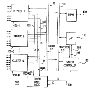
A block diagram of an ATM switch 100 constructed in
10 accordance with the principles of the present invention is shown
in Fig. 1. Switch loo comprises a microprocessor 1l0, a switch
controller 120, DRAM memory 130, token grant logic 140, and port
clusters 150-1 to 150-n. Each port cluster 150-k contains the
line interfaces, port logic, and buffering for up to eight ATM
15 network connections. All of these functional blocks, with the
exception of token grant logic 140, are interconnected by
processor bus lSo. Processor bus 160, shown as a single bus in
Fig. 1 for the sake of clarity, actually comprises three
separate physical buses: a data bus, an address bus, and a bus
20 carrying system timing and control signals. References to
processor bus 160 below are intended to indicate the data bus,
unless otherwise noted. Bus cycles along processor bus 160 are
generated either by microprocessor 110 itself or by switch
controller 120, as described in more detail below. In addition,
25 port clusters 150-1 to 150-n are interconnected via a switch bus
170, operating at 32 MHz, along which ATM cell copying is
performed.
The grouping of up to eight individual ATM ports into a
single port cluster 150-k is intended to eliminate the need for
30 complex bus circuitry. A single bus connecting all ports of a
large switch would require costly high-performance bus drivers
to meet the necessary loading re~uirements. Additionally, a bus
physically long enough to connect all the ports would be
susceptible to bus reflections, attenuation and noise problems
35 which could only be corrected with sophisticated bus design.
The present invention employs a hierarchical bus structure to
eliminate these difficulties and permit the use of cost-
-- 10 --
-
CA 02233~ 1998-03-30
W097/13377 PCT/GB96/02362
effective components. As shown in Fig. 2, each port cluster
~50-k contains its own local processor bus 250 and switch bus
240 interconnecting the ports 210-1 to 210-n of that cluster.
The cluster 150-k of Fig. 2 is shown with a full complement of
5 eight individual ports, but fewer ports may be installed. Bus
loading on these local buses is manageable since, in the
preferred embodiment, a ma~irll~ of eight ports will be resident
in a single cluster, and presumably, bus lengths will be short
because clustered ports can be expected to be physically located
10 together. Data passing between the ports 210-1 to 210-n of an
individual cluster 150-k, therefore, should not encounter any
significant bus degradation.
Referring now to both Figs. 1 and 2, cell data is delivered
from cluster 150-k to cluster 150-1 by switch bus 170. Local
15 switch bus z40 in each cluster 150 is coupled to switch bus 170
through bidirectional bus transceiver 260. Bus transceiver 260
is designed such that data traveling out of cluster 150-k is
latched onto switch bus 170, and data travelling from switch bus
170 into cluster 150-1 is buffered. This ir.troduces a one clock
20 cycle delay between availability of the data within cluster 150-
k and availability of the data in the other clusters including
cluster 150-1. The control signals are delayed correspondingly.
However, this additional complexity is intended to counter any
settling time problems which might otherwise occur. Likewise,
25 local processor bus 250 is connected to processor bus 160
through bidirectional bus transceiver 270. In this fashion,
heavily populated buses are kept relatively short, while the
longer switch bus 170 and processo- bus 160 have few
connections. Advantageously, inexpensive bus drivers may be
30 used and complex electrical bus conditioning need not be
performed.
As the principal task of switch 100 is to route ATM cells
from a plurality of input links to a plurality of output links,
a description of a typical ATM cell would aid in comprehending
35 the present invention. Fig. 3A shows the format of an ATM cell
300 as defined in CCITT Recommendation I.361. This format,
adopted for use in B-ISD~ and othe- wide-area networks,
-- 11 --
_
CA 02233s~ 1998-03-30
WO97/13377 PCT/GB96/02362
specifies a cell of 53 bytes: an information field or payload
3 ~ of 48 ~ytes which contains the user information which is the
object of the transmission and a cell header 320 of 5 bytes.
Cell header 320, or simply "header", is used for
5 transmitting a variety of control information regarding the
instant cell. Fig. 3B shows the structure of this header at the
User Network Interface ("UNI"), that is the interface between
an end-user device and an ATM switch. Here, the header is made
up of a Generic Flow Control ("GFC") field 330 for specifying
lO information which may be used to control traffic flow at the
user-network interface, a virtual path identifier ("VPI") 340,
a virtual circuit identifier ("VCI~) 350, a Payload Type
Identifier ("PTI") field 36~ which provides information
regarding the type of information contained in payload 310 of
15 the cell, Cell Loss Priority ("CI.P"~ flag 370 for setting the
priorities relating to the abandonment of the cell during
overload conditions, and a Header Error Control ("HEC") field
3~0 which contains an error control checksum for the previous
four bytes in header 320.
Fig. 3C shows the format of header 320 at the Network-to-
Network Interface ("NNI"), the interface between network
switches. This header structure is identical to the structure
at the UNI except GFC 330 is replaced with four additional bits
of VPI 340. ATM networks do not provide for flow control of the
25 type which is implemented in some packet networks and ATM
networks have no facility to store cells over a long period of
time. Therefore, inside an ATM network there is no need for
generic flow control. Thus, GFC 330 may be eliminated in favor
of an expanded VPI 340. However, if eight bits of VPI are
30 sufficient, the header 320 of Fig. 3B may be used throughout the
network. For more information regarding standard ATM cell
formats see de Prycker, pp. 124-28. Of course, when alternative
packet networks are implemented, a cell may be a packet or any
other way to provide a collection of data on a network.
one skilled in the art will recognize that alternative
fixed cell sizes are possible for use in an ATM LAN. However,
because interoperability between local networks and wide area
- 12 -
CA 022335~5 1998-03-30
W O 97/13377 PCT/GB96/02362
services is desirable, use of the standard 48-byte payload size
is recommended. However, header size and format are not
critical for interoperability with existing networks because
headers are typically modified by ATM switches, while payloads
5 are passed unaltered from one point to another. Therefore,
header formats other than those shown in Figs. 3B-3C may be
utilized. See Dimitri Bertsekas & Robert Gallager, Data
Networks (2nd ed., Prentice Hall, Englewood Cliffs, New Jersey,
1992), pp. 37-141, for examples of a variety of header
10 structures suitable for use in a wide range of networ~
technologies.
In an ATM network, information, such as audio, video and
data, is transmitted by the cells through virtual paths and
virtual circuits which are set up to facilitate such
15 communications. The use of virtual paths and virtual circuits
allows a large number of connections to be supported on a single
physical communications link. The virtual paths comprise a
plurality of virtual circuits which share the same physical
resources through at least a portion of the network. Virtual
20 paths/virtual circuits are allocated during set-up of a
communication transmission between two network clients and are
"torn down" after the communication has completed.
An ATM switch must accomplish two tasks when it receives
a cell on an input port: (1) translation of the header
25 information in the cell; and (2) transport of the cell from the
input port to the correct output port. Proper translation of
the routing identifiers, the VPI and VCI values, in the header
is important because in a standard ATM network, although these
values correspond to a virtual path or virtual circuit passing
30 through the network, the values only have local significance.
Therefore the VPI/VCI data is translated by each switch and
changed prior to the cell being output from the switch. This
translation is accomplished throu~h the use of translation
tables which are loaded with proper values when the connection
35 is initially established. Much of the discussion which follows
describing the switching functions of the present invention
assumes that these translation tables have been properly created
- 13 -
CA 02233~5~ lsss-03-30
WO97/13377 PCT/GB96/02362
during connection set-up time under the auspices of
microprocessor 110.
In operation, ATM cells are received by switch 100 via an
ATM line interface 405 as shown in Fig. 4. Fig. 4 illustrates
5 a block diagram of an individual port 210-i. The actual
composition of line interface 405 depends upon the physical
medium from which the ATM network is constructed. In the
preferred embodiment line interface ~05 connects via an RJ45
connector 410 to a 25.6 Mb/s ATM full-duplex link 400. The 25.6
lO Mb/s ATM physical layer is an ideal platform for most ATM
networks operating in a LAN setting. cabling requirements can
be met with the ubiquitous voice-grade UTP 3 (Unshielded Twisted
Pair) cable and widely used UTP 802.4 Token Ring physical layer
components may be used to construct line interface 405. Signals
15 from RJ45 connector 410 are passed through filter 415 to be
delivered to Physical Media Dependent ("PMD") chip 420.
Although a 25.6 Mb/s physical link is employed in the preferred
embodiment, one skilled in the art will recognize that a wide
variety of physical layers may be used. For example, the 25.6
20 Mb/s port may be replaced by a lOO Mb/s port or a 155 Mb/s port.
Nor is there any requirement that all ports within switch lOO
operate at the same speed. Therefore, one port may operate at
lOO Mb/s while the others remain at 25.6 Mb/s. Of course, the
components of line interface 4Qs must be altered to be
2S compatible with the chosen ATM physical link. Only line
interface 405 need be changed, as all other aspects of port 210-
i and switch 100 can remain the same. It will be recognized,
however, that to service a large number of high speed ports
(e.g., 155 Mb/s) bus and processor speeds within the switch
30 would need to be increased.
A new ATM cell arriving on input link 400 is converted from
electrical signals to a bitstream by PMD chip 420. The
bitstream is provided to network control logic 430 which begins
the processing of the incoming cell. Network control logic 430
35 calculates a checksum from the first four bytes of cell header
320 and compares this value to the fifth byte, HEC 380, of
header 320. If the values do not match an error has occurred
- 14 -
CA 02233~ 1998-03-30
WO97/13377 PCT/GB96/02362
in header 3Z0 during the cell's journey from the previous node
in the network. Since misdirected cells are unacceptable in an
ATM network, network control logic 430 will discard the entire
incoming cell.
Alternatively, the checksum may be a more complex
calculation which will permit some limited correction of single-
bit header errors. However, current B-ISDN standards specify
correction of isolated single-bit errors and discard of burst
errors. This specification can be implemented by a simple state
lO machine as shown in de Prycker, pg. 123 or Bertsekas, pg. 134.
If desired, such a state machine may be implemented in network
control logic 430 by methods well known in the art.
Assuming that no errors are detected in the header or that
any errors have been successfully corrected, network control
15 logic 430 will place the first four bytes of the header in
receive FIF0 440 followed by the 48 bytes of the cell's
information payload. Note that no error checking is performed
on the information payload. Network control logic 430 will not
place the HEC 380 byte in receive FIFO 440, rather it will
20 discard it. The HEC 380 byte is not required within the switch
i~self and because the switching processor normally modifies the
header, a new HEC 380 byte will need to be generated when the
cell is again transmitted. Therefore, the received HEC 380 byte
may be discarded immediately after the integrity of the cell
25 header is established.
In the preferred embodiment, receive FIFO 440 is a 512 X
32 dual port SRAM, therefore capable of storing up to thirty-
nine (39) received ATM cells at any one time. Network control
logic 430 may continue to place cells into receive FIFO 4~0
30 until the buffer is full, whereupon additional cells will be
discarded. It should be noted that although network control
logic 430, receive FIFO 440 and other port components are shown
as discrete components, much of this circuitry may be placed on
a single Application Specific Integrated Circuit ("ASIC").
Those skilled in the art will recognize that a wide range
of FIF0 sizes may be employed, some being more suitable for some
implementations than others. However, currently SRAM memory is
-- 15 --
CA 02233~ 1998-03-30
WO 97/13377 PCT/GB96/02362
extremely expensive. Therefore, implementatlons requiring large
SRAM buffer sizes may be too costly to be successfully installed
in LAN environments. Alternative methods for handling switch
c_naestion, such as the derailing method described below, may
5 be employed to achieve acceptable cell loss probabilities, while
still permitting small, cost-effective FIF0 memories.
The placement of the first complete s2-byte cell in receive
FIF0 ~40 will be detected by port control logic ~50. Port
control logic 450 will assert REQUEST ~90 to re~uest service of
10 the queued cell by the switching architecture.
A request for service by a port 210-i initiates the entire
s~itching operation. A switch cycle, that is, the transfer of
a single ATM cell from an input port 210-i to an output port
210-j, is comprised of three distinct phases: input port
15 selection, header processing, and cell copying which occur in
that order. These phases, as will be more fully described
below, operate both serially and simultaneously. ~or instance,
as the cell copying phase of one switch cycle is being
performed, the header processing phase of the next switch cycle
20 will be occurring, and at the same time the input port of the
following switch cycle is being selected. Advantageously, this
arrangement yields a significant increase in switching
throughput over conventional switch designs which process a
single incoming cell at a time.
A request for service is processed in the following manner.
As shown in Fig. 2, the ports of a cluster 150-k are
conceptually divided into an lower ban~ 220 and an upper bank
230. REQUEST 490 is wire-ored together with request signals
from the other ports belonging to the same bank to form
30 REQUEST_L0 280 or REQUEST UP 290. As will be illustrated below,
the division of ports into separate banks permits relatively
simple port identification and addressing. It will be
recognized, however, that the principles of the present
invention may be practiced without employing this type of port
35 division.
Port requests for service are arbitrated by a token bus
scheme managed by the token grant logic 1~0. Referring again
- 16 -
CA 02233~ 1998-03-30
WO97/13377 PCT/GB96/02362
to Fig. 1, all pending port requests 175, which contains
REQUEST_L0 280 and REQUEST_UP 290 from all clusters lS0-1 to
150-n~ are ~ined during an active sample period. When one
or more ports have asserted REQUEST 4~0 the token grant logic
5 will assert a GRANT signal 180 to one of the clusters 150-k
whose REQUEST_L0 280 or REQUEST_UP 290 is asserted. Within
cluster l5o-k GRANT 180, which represents the token, will be
passed in se~uence between the cluster ports 210-1 to 210-n
until it is received by requesting port zlo-i. This port 210-i
10 will be granted access to the switch bus during the next
switching cycle.
Upon receiving the token, port 210-i communicates an ID
number to token grant logic 140. The individual ports deliver
only a two bit ID number via cluster ID bus 185 which identifies
15 the requesting port within its port bank, upper or lower. Token
grant logic 140 combines this information with its knowledge of
which request line generated the grant (which implicitly
identifies the cluster 150-k and the port bank). Token grant
logic 140 then creates an ID number unique to that port within
20 the entire switch. Alternatively, the port may be implemented
to communicate its full ID number. In the preferred embodiment,
ID numbers are assigned such that lower ID values (0-15) are
assigned to ports resident in lower banks, and higher values
(16-31) to ports in upper banks. This arrangement, as further
25 described below, permits all lower bank (or upper bank) ports
to be selected to receive the cell in a single multicast
switching operation. This ID number is placed on the switch ID
bus 190 to be delivered to switch controller 120. The token
grant logic 140 then delivers a switch cycle request to
30 microprocessor 110 to notify it of the presence of a selected
port with data to transfer. In the preferred embodiment, this
request is performed by means of a processor interrupt, though
other signalling methods may be used. For example, the
processor might routinely monitor a status register.
Microprocessor 110 is, preferably, a commercially available
RISC single-chip microprocessor such as the ARM610, manufactured
by Advanced RISC Machines of Cambridge, England, operating at
- 17 -
CA 022335~5 1998-03-30
W O 97/13377 PCT/GB96/0236232MHz with a memory bus speed of 16MHz. If the switch is in
normal operation, microprocessor 110 will respond to a switch
cycle request by asserting SWITCH_CYCLE_START 193 to notify
switch controller 120 to initiate a switch cycle.
5 SWITCH_CYCLE_START 193 is shown as a single signal line in Fig.
1, but a variety of methods might be employed to deliver the
cycle request to switch controller 120, such as a processor
signal or setting a status register bit. In the preferred
embodiment microprocessor 110 actually executes a two word
10 memory read instruction directed to a fixed address continually
monitored by switch controller 120.
Although the majority of cells switched by switch lOo will
be serviced almost entirely by hardware, it is important that
each switch cycle be initiated under the authority of
15 microprocessor 110 via SWITC~_CYCLE_START 193. Microprocessor
110 may frequently have to respond to signalling and management
cells requiring updates to the routing tables ultimately used
by switch controller 120. A switch cycle cannot be permitted
to occur while these updates are in progress. Microprocessor
20 110 accomplishes this by simply refusing to respond to a switch
cycle reguest until such updates are complete. This obviates
the need for the complex interlocks which might be required if
the switching hardware operated independently of processor
control.
Switch controller 120 is a hardware coprocessor which
manages the switching operation. Switch controller 120 is
actually a sequential state machine which may be constructed
using well-known digital design techniques using discrete logic,
gate arrays, or ASICs. Preferably, however, switch controller
30 120 is a commercially available field programmable gate array,
such as the XC4010D manufactured by Xilinx Inc. of San ~ose,
California. Field programmable gate arrays provide the
capability of modifying and updating switch controllèr 120 while
the unit is installed within an ATM network. Such capability
3~ will be essential for the foreseeable future, as standards for
ATM LAN networks have not been completely defined. The use of
- 18 -
CA 02233~ 1998-03-30
WO 97/13377 PCT/GB96/02362
easily modified technology will permit users to adopt ATM LAN
networks without fear of lost investment.
Both microprocessor 110 and switch controller 120 reside
on the same processor bus 160. Switch controller 120 can not
S utilize processor bus 160 to perform switching functions while
microprocessor 110 is active without encountering unacceptable
bus contention. Therefore, after detecting ~wll~n_ CYCLE_START
193, switch controller 20 asserts PROCWAIT 195 which, tied
directly to the processor wait input line of microprocessor 110,
10 places microprocessor 110 into a wait state. Switch controller
120 also disables the processor bus, thereby eliminating any
possible bus conflict difficulties.
After asserting PROCWAIT 195, switch controller 120
initiates an OLD HEADER read cycle to all switch ports. All bus
15 cycles originated by switch controller 120, including the OLD
HEADER read cycle, mimic an actual microprocessor 110 bus cycle.
The nature of the instant read cycle is communicated to the
ports by switch controller 120 via the assertion of the
OLD_HEADER signal 492 as shown in Fig. 4. This signal, as well
20 as NEW ROUTE ~94, NEW HEADER 496 and CELL COPY 498 are generated
by switch controller 120 but are not shown in Figs. 1 and 2 for
the sake of clarity. In response to OLD_HEADER 492, port
control logic 450 of port 210-i which has current possession of
the token will remove the cell header from the first cell in its
25 receive FIEO and place it onto processor bus 160 (through local
processor bus 250). As discussed above, the HEC 380 byte is no
longer in the cell header, as it was previously removed by
network control logic 430. Advantageously, the remaining four
header bytes can be accessed by a single read operation on 32-
30 bit processor bus 160.
When the cell header is present on processor bus 160 andbeing read by switch controller 120 the port control logic 450
of all ports will latch the header in their respective old
- header latch 455. This information will be used by the ports
35 to create a new outgoing header, as further described below.
At the completion of the OLD HEADER read cycle, the selected
port releases the token. The token is again passed from port
- 19 -
CA 022335~5 1998-03-30
W O 97/13377 PCT/GB96/02362 to port within the cluster via GRANT 180 until it reaches the
next port in need of service within the cluster. Note that
within a single port GRANT 180 is composed of two signals
GRANT_IN 486 and GRANT_OUT 488. If no other ports require
5 service within the cluster, token grant logic 140 will assert
GRANT 180 to another cluster containing a port whose request was
received during the last active sample period. That port will
reguest a switch cycle in the same manner as described above.
In this fashion, port selection for the next switch cycle is
10 accomplished during the header processing phase of the previous
cycle. If no requests remain, another sample will be taken.
Only the ports requesting service during an active sample
period will be serviced. Other ports with cells which become
ready after the sample period must wait until the next sample
15 period. This imposes a form of arrival scheduling without
comple~ logic.
Once the cell header has been latched by switch controller
120, the switch cycle enters the header processing phase.
Initially, switch controller 120 performs an e~;nation of the
20 header value. If the header was at some point corrupted and now
no longer contains a reasonable value, switch controller 120
will abort the switch cycle and discard the cell. A variety of
methods of checking the header information are available and
will be obvious to those of skill in the art. However, a crude
25 integrity check on the header may be performed by verifying that
the four bits of GFC 330 are set to zero. Recall that GFC 330
is defined only at the UNI and is available to help the user to
statistically multiplex the cells from different applications
onto the access link to the network. GFC 330 will be set to
30 zero by the user when the cell is transmitted onto the network.
If the eight bits of VPI 340 are sufficient for the network
implementation, rather than the full twelve normally available
in the NNI, than GFC 330 may be used for error check purposes.
If switch controller 120 detects a non-zero GFC 330, then the
35 header must have been corrupted. Switch controller 120 will
generate an exception condition, as described below, requesting
microprocessor 110 to assume control of the switching
- 20 -
CA 02233~ 199X-03-30
WO97/13377 PCT/GB96/02362
architecture to remove the remainder of the corrupted cell from
the receive FIFO 440 of port 210-i. However, if the value
appears sensible, switch controller l20 will perform some
initial processing which will ultimately guide the overall
5 course of the switch cycle.
TAB~E I - PAYLOAD TYPE BIT ~.-lN~8
000 Normal data cell
00l Data cell with user data bit set
0l0 Normal data cell/experienced congestion
0ll Data cell with user data bit
set/experienced congestion
100 Segment F5 OAM (Operation and Management)
cell
l0l End-to-end OAM cell
ll0 Resource management (flow control) cell
lll Signaling cell (no defined use)
Switch controller 120 will examine PTI 360 to determine
20 whether the instant cell carries a normal user information field
or whether the cell is a signalling or management cell intended
to be received by the switch itself. The bit definitions of PTI
360 are shown above in Table I. If PTI 360 contains a value 0,
l, 2 or 3, then the cell is a normal data cell requiring a
25 typical switching operation. Cells with values 5 or 6 are end-
to-end signaling cells which will also be passed straight
through. The value 7 is currently undefined, so these cells
will also receive normal handling. Cells containing a PTI 360
of 4 are link level Operation and Management ("OAM") cells which
30 require special processing by microprocessor ll0. These values
will result in an exception handling procedure as described
below. Switch controller 120 also inspects VCI 350 to detect
link level OAM cells identified by a VCI value of 3. These also
require special processing by microprocessor ll0, and likewise
35 will result in an exception handling procedure.
If the header indicates that the cell requires normal
switching, switch controller 120 will ~x~mine VPI 3~0. If VPI
- 21 -
CA 02233555 1998-03-30
PCT/GB96/02362
W O 97/13377
3~0 is equal to zero, the cell is a member of a typical
unbundled virtual circuit and will require ordinary switching.
A non-zero VPI 340 on the other hand indicates that the cell's
virtual circuit is a member of a virtual path, which should
5 undergo virtual path switching. Performance of virtual path
switching is described below.
If the cell carries a normal payload and VPI 340 is zero,
switch controller 120 extracts VCI 350 from the header. As
shown in the flow diagram of Fig. 5, the sixteen bits of VCI 350
10 are hashed together with the five bits of Port ID 510
identifying the selected input port 210-i provided by token
grant logic 140 via switch ID bus 190. This hash function
produces a sixteen-bit routing table index 530.
The actual hash function used to create the routing table
15 index is shown in Fig. 6A. The sixteen bits of VCI 350 are
exclusive-ored with a sixteen bit value formed by the port ID
510 in the 5 most significant bits followed by 11 ~eroed bits.
The use of hash functions to generate table indexes is a well-
known technique in computer science and is described in a
20 variety of references. See, e.g., D.E. Knuth, The Art of
Computer Programming, Vol.3, ~Addison-Wesley Publishing Company,
Reading, Massachusetts, 1973) and Alfred V. Aho, John E.
Hopcroft, and Jeffrey D. Ullman, The Design and Analysis of
Computer Al gori thms (Addison-Wesley Publishing Company, Reading,
25 Massachusetts, 1974), pp. 111-13. Those skilled in the art will
recognize that the present invention is in no way limited to the
use of a particular hash function, but rather that anyone of a
wide variety of hash functions may be utilized.
In order to perform the cell header translation required
30 in all ATM switches, a routing table is needed which maps the
incoming port and header values to outgoing port and header
values. As shown in Fig. 7, the routing table 720 of the
present invention is stored in DRAM memory 130. DRAM memory 130
also contains the basic switch operating software 710 executed
35 by microprocessor 110, and special processing routines 73Q and
derail buffer 740, whose respective functions will be described
below.
- 22 -
CA 02233~ 1998-03-30
WO97/13377 PCT/GB96/02362
The base address 520 in DRAM 130 of routing table 720 is
added to the routing table index S30 generated by the hash
function to produce a specific address within routing table 720.
Switch controller 120 initiates a two word memory read at this
5 address which obtains two distinct values: the Route Word 540
and the New Header Word 550. These values will have been placed
in routing table 720 previously by microprocessor llO when the
virtual circuit corresponding to the instant cell was initially
established.
One of the principal motivations behind employing a hash-
based routing table is the efficient use of table memory. To
fully comprehend the benefits of hash indexing, the
establishment and management of routing table 720 at connection
set-up time must be examined.
lS As mentioned above, ATM is a connection-oriented
technology. When an end node wants to communicate with another
end node, it requests a connection to a destination node by
transmitting a signalling request to the network. The request
is passed through the network, that is, through the ATM
20 switches, until it reaches the destination node. If the
destination and the network nodes all agree that sufficient
bandwidth is available to maintain the connection, a virtual
circuit will be formed.
When the connection is being established each switch must
25 create an entry in its local routing table 720 which contains
the information necessary to identify a cell as belonging to the
virtual circuit and the information necessary to modify the
headers of cells of that virtual circuit passing through the
switch. This includes, at a ~; n i 1~, the incoming port number,
30 incoming VCI/VPI, outgoing port number, and outgoing VCI/VPI.
The VCI/VPI values only have local significance. The switch
will choose the incoming VCI/VPI and provide the previous switch
in the circuit with that information; the outgoing VCI/VPI will
be provided by the next node in the network.
One of the major disadvantages of conventional ATM switches
is the need to maintain a large routing table for each port of
the switch. Normally, however, most ports of an ATM switch will
- 23 -
CA 02233~s~ 1998-03-30
WO97/13377 PCT/GB96/02362
only service a small number of virtual circuits at any one
instant in time, while a few ports will handle a large volume
of different traffic. Each table must be large enough to
accommodate the significant number of circuits which may be
5 present at any one time on any one port, but this memory will
be left idle during much of the switch operation. This is a
very inefficient use of memory, which can be the most costly
component of the switch.
In the present invention, however, switch controller 120
lO indexes the routing table using a hash function, thus permitting
the use of a smaller shared routing table. If only low VCI
values are used, the index will be into a small logical routing
table dedicated to that input port. In the preferred
embodiment, this logical routing table contains enough table
15 space to specify 2048 virtual circuits. However, if a larger
range of VCI values is used, or if VPIs are used, switch
controller 120 permits the logical routing tables for different
ports to share memory in a controlled way.
When the virtual circuit connection is established, the
20 si~nalling software executed by microprocessor llO will select
an initial VCI (or VPI) value. Microprocessor llO will check
to see if the hash function, using that VCI and the input port
ID, would generate an index pointing to a location in routing
table not currently used by another virtual circuit. If the
2~ table location is currently occupied, the VCI value will be
changed to a value which, when input to the hash function, will
generate an index which will point to a free location. This VCI
value will be transmitted to the previous node on the virtual
circuit with instructions to place it in the outgoing cell
30 headers. In this fashion the routing table memory may be
shared, eliminating the need for large, under-utilized memories.
Although hash-table allocation is performed locally in the
preferred embodiment, it will be recognized by those of ordinary
skill in the art that such allocation may be performed remotely
35 by a centralized network signalling processor. In this
configuration, allocation information will be transmitted to the
- 24 -
CA 02233~ 998-03-30
W097/13377 PCT/GB96/02362
~witch via signalling and management cells by the central
processor itself.
The Route Word is the principal vehicle by which
information concerning the proper flow of the switch cycle is
5 communicated to microprocessor 110 and ports 210-1 to 210-n.
As shown in Fig. 8, Route Word 540 is a 32-bit word conceptually
separated into two 16-bit portions. The lower 16-bit portion
805 contains a variety of control information which direct the
proper h~n~ ing of the instant cell, whereas the upper 16-bit
lo portion 810 provides a mechanism for identifying the proper
output port or ports 210-j to receive the cell being switched.
At this point the Route Word 540 and the New Header Word
550 are delivered to microprocessor 110. Recall that
microprocessor 110 initiated the switch cycle by executing a two
15 word memory read at a fixed address. Switch controller 120 will
release microprocessor 110 from the wait state ~y removing
PROCWAIT 195. As microprocessor llo completes this read cycle,
switch controller 120 generates memory cycles which place the
Route Word 540 and New Header Word 550 onto processor bus 160
20 so that microprocessor 110 receives these values as a result of
the read operation.
Microprocessor 110 will ~ne the Route Word to determine
if special processing during this switch cycle is required.
Specifically, microprocessor 110 will inspect CONTROL CODE 815
25 contained in the first three bits of Route Word 540 as shown in
Fig. 8. The possible values of CONTROL CODE and their
respective meanings, as employed in the preferred embodiment,
are shown below in Table II.
- 25 -
CA 02233555 l998-03-30
WO97/13377 PCT/GB96/02362
TABLE II - CONTROL CODE BTT x~ hGS
BIT 2-0 OPERATION
O O O Exception, Count Cell
0 0 1 Exception
O l O Normal Switch Cycle,
Count Cell
O 1 1 Normal Switch Cycle
1 O O Derail Cell, Count Cell
1 0 1 Derail Cell
1 1 0 ___
1 1 1 ___
In a normal switch cycle CONTROL CODE 815 will be set to
15 'O11' indicating that no special processing by microprocessor
110 need be performed. The other possible values of CONTROL
CODE 815 specify special functions, the processing of which will
be described in detail below.
Switch controller 120 inspects the SWITCH COMMAND field 870
20 of Route Word 540 to determine the action it needs to take
during the switch cycle. The possible values of SWITCH COMMAND
and their respective meanings, as employed in the preferred
embodiment, are shown below in Table III.
- 26 -
CA 02233555 l998-03-30
PCT/GB96/02362
W O 97/13377
T~UB~E III - 8WITCH C~MM~ ~ BIT ~TTINGS
BITS 9-7 OPEFU~ION
0 0 0 Do Nothing
50 0 1 ~h~h
0 1 0 Indirect
0 1 1 Extend
1 O O Go (Normal Switch
Cycle)
101 0 1 Escape 1
1 1 0 Escape 2
1 1 1 Escape 3
Value 'Go' indicates a normal switch cycle. Value 'Do
15 Nothing' is used when the cell will be processed entirely by the
software, and instructs switch controller 120 to take no further
action after delivering Route Word 540 and New Header Word 550
to microprocessor 110. Such an instance may occur when a cell
is received that is destined for the switch itself, as described
20 below. Other values indicate that special action is required
by switch controller 120, and are described in more detail
below.
When switch controller 120 reads Route Word 540 from
routing table 720 all ports 210 except the current input port
25 210-i also read Route Word 540 by latching it from processor bus
160 (through local processor bus 250) into their respective
Route Word Latch 457. Switch controller 120 identifies the
presence of Route Word 540 on processor bus 160 by asserting NEW
ROUTE signal 494. The ports read Route Word 540 simultaneously
30 with switch controller 120 to eliminate the need for a separate
bus cycle to deliver the information of Route Word 540 to the
ports. As with the simultaneous reading of the Old Header, this
arrangement has the advantage of significantly increasing the
speed of the switching cycle.
35Each port e~mines Route Word 540 to determine whether it
is the intended recipient of the cell being switched. As shown
- 27 -
CA 02233~S 1998 - 03 - 30
PCT/GB96/02362
WO 97J13377
in Fig. 8, the bits of the upper 16-bits 810 of Route Word ~40
indicate which output port 210-i should receive the cell. A
port will recognize that it is the intended output port 210-j
when it sees its corresponding bit set. Ports resident in the
5 lower banks of each cluster are addressed when UpLo 865 of the
lower portion 805 of the word, also shown in Fig. 8, is zero,
whereas the ports in the upper banks are addressed when UpLo 865
is one. The selected output port 210-j will use the remaining
bits of the lower portion 805 of Route Word 540 to determine the
10 proper disposition of the New Header Word 550 and the cell
payload.
When the New Header Word 550 is read onto processor bus 160
by switch controller 120, only port 210-j selected by Route Word
540 to be the output port will latch the New Header Word 550
15 into its New Header Latch 459. Switch controller 120 identifies
the presence of the New Header Word 550 on processor ~us 160 by
asserting NEW HEADER signal 496. The format of New Header Word
550 is identical to the standard ATM cell header format depicted
in Figs. 3B and 3C. Port control logic 450 will use the field
20 values in the New Header Word 550 to modify the Old Header
stored in old header latch 455 to construct the proper new
header for the outgoing cell. Specifically, port control logic
450 will ~ ;ne the fields New VPI 850 and New VCI 855 in Route
Word 540 to make the proper substitutions. If one of these bits
25 is set then port control logic will substitute the corresponding
new value of that field in the New Header Word 550 in the
outgoing header. For example, if New VCI 855 is set, then the
~CI 350 in the New Header Word 550 will be used in the outgoing
header, while all other fields will remain identical to those
30 in the old header. Set CONG 845 flag instructs the port control
logic 450 to translate the PTI 360 field of the outgoing cell
to mark the cell as having experienced congestion as shown in
Table I. Likewise, the Set CLP ~40 flag instructs port control
logic 450 to set CLP 370 in the outgoing cell.
The issuance of the Route Word 540 and New Header Word 550
to microprocessor 110 completes the header processing phase of
the switch cycle. At this point, assuming no errors or
- 28 -
CA 02233~ 1998-03-30
WO 97/13377 PCT/GB96/02362
conditions requiring microprocessor intervention have been
detected, and SWITCH COMMAND 870 contains the Go CG ~n~, switch
controller 120 will initiate the cell copying process by
asserting CELL COPY signal 498. In response to this signal the
5 selected input port 210-i will place the twelve words of the
cell payload onto switch bus 170 in a sequential fashion. The
selected output port 210-j will read the twelve words from
switch bus 170, concatenate those words with the new header
which it has constructed and place the complete cell into the
10 proper transmit FIFO, as described below. As cell copying is
being performed along switch bus 170 (and/or local switch bus
240), the header processing phase of the next switch cycle will
begin utilizing processor bus 160.
Two transmit FIFOs 480, 485 are employed in each port 210,
15 rather than the typical single FIFO, to achieve a simple form
of prioritization of transmission. FIFO 480 is the high-
priority, or real-time, queue, whereas FIFO 485 is the low
priority, or non-real-time, queue. Cells travelling on high
quality of service virtual circuits, such as circuits carrying
20 multimedia video and audio streams, may be placed into the high-
priority transmit FIFO 480 to await transmission, while cells
on circuits with less stringent timing requirements may be
placed in the low-priority FIFO 485. The determination of which
queue should be used for a particular virtual circuit is made
25 at connection set-up time.
In the preferred embodiment, each transmit FIFO 480, 485
is a 256 X 32 dual port SRAM, each capable of storing nineteen
(19) complete ATM cells. Therefore, a m~i of thirty-eight
(38) cells may be queued for transmission within a single port
30 210 at any one time. Of course, as with the input FIFOs 440 a
wide range of buffer sizes may be employed, and if other
overflow handling methods are not implemented larger queue sizes
~ill be required to achieve acceptable cell loss probabilities,
~ut at a significant component cost.
~5 Port control logic 450 of output port 210-j determines
which transmit FIFO to place the outgoing cell by examining the
Priority bit 860 of Route Word 540. If Priority 860 is one,
- 29 -
CA 022335~5 1998-03-30
W O 97/13377 PCT/GB96/OZ362 then the cell will be placed in the high-priority FIFO ~80,
otherwise the cell is placed in the low-priority FIFO 485.
Output port 210-j will transmit all cells residing in the high-
priority FIFO 480 before it transmits any from the low-priority
5 FIFO 485. In this fashion, more urgent traffic is serviced in
a more timely manner. Those skilled in the art will recognize
that this is not the only selection scheme and that other
mechanisms can be implemented. For instance, a better
utilization of the available buffer space can be made by
10 alternately servicing both FIFOs until high-priority fifo 480
reaches some predefined level of occupancy, whereupon high-
priority FIFO 480 is then serviced exclusively.
Once at least one cell resides in one of the transmit FIFOs
480, 485, network control logic 430 will begin transmission of
15 that cell onto the outgoing network link 400. Network control
logic 430 will deliver the cell to line interface 40S beginning
with the first four bytes constituting the cell header. Network
control logic 430 will calculate an appropriate checksum for
these first four bytes and will transmit that error check byte,
20 HEC 380, as the fifth byte of the cell transmission. The
remaining 48 bytes of the cell constituting the cell payload
will then be transmitted. Once the complete cell is transmitted
by the line interface, the switching operation regarding that
specific cell is complete.
Advantageously, switch controller 120 can accomplish
virtual path switching as easily as virtual circuit switching.
A virtual path is a collection of separate virtual circuits of
the same quality of service which are travelling along the same
route for at least part of their journey. A virtual path is
30 specified by a non-zero value in VPI 340 of a cell header 320,
as shown in Fig. 3. Because switching on a single VPI 340 value
can switch cells from a large number of virtual circuits,
routing table sizes in DRAM 130 can be kept relatively small.
Combining virtual circuits into a single virtual path is called
35 encapsulation.
A cell belonging to a virtual path is switched by switch
controller 120 in the same manner an ordinary cell is switched.
- 30 -
CA 02233~ 1998-03-30
wos7/13377 PCT/GB96/02362
However, switch controller 120 will detect the non-zero VPI 340
in the cell header 320, and use that value rather than the value
of VCI 350 to create the routing table index. As shown in the
flow diagram of Fig. 9, switch controller 120 will hash the
5 eight bits of VPI 340 with the five bits of Port ID 510
identifying the selected input port 210-i provided by token
grant logic 140. This hash function will generate a sixteen-bit
routing table index s30.
As shown in Fig. 6B, however, a separate hash function is
lO employed when switching on the VPI 3~0. In this hash function,
the sixteen-bit index is directly created by placing the port
ID 510 value in the 5 most significant bits, setting the next
three bits to one, and placing the VPI 340 value in the lower
eight bits. Note that an alternate hash function will be
15 required if twelve-bit VPI standard of the NNI is employed. The
base address 520 of the routing table is added to the table
index 530 to produce a specific address within the routing
table. Note that by using a hash-based method, in contrast to
conventional ATM switches, VPIs and VCIs can be maintained
20 within the same routing table thereby conserving memory space.
As in a VCI switching operation, switch controller 120 initiates
a two word memory read at this address to obtain the Route Word
540 and the New Header Word 5SO. The remainder of the switch
cycle will occur in precisely the same way as an ordinary switch
25 cycle.
A more complicated operation will occur when switch lOO
must perform virtual path de-encapsulation. A virtual path will
need to be broken into its constituent virtual circuits when it
reaches its end point. Although each cell belonging to the
30 virtual path will arrive at the switch with a non-zero VPI 340,
switch controller 120 must recognize that the virtual path is
at its end and switch on the VCI 3SO value instead.
The flow diagram of Fig. lO illustrates this operation.
As before, VPI 340 is hashed with the port ID 510 to obtain a
35 table index 530 used to retrieve the Route Word 540. The SWITCH
COMMAND field 870 of Route Word 540 will be set to the Rehash
command as specified in Table III, indicating to switch
- 31 -
CA 02233~5 1998-03-30
PCT/GB96/02362
WO 97/13377
controller 120 that a second h~.~h i ng operation mu5t be
performed. Note that New Header Word 550 is not shown at this
point in the flow diagram of Fig. 10. Although switch
controller 120 will execute a two word memory read, the second
5 word obtained will have no sensible value. Upon detecting the
Rehash command in SWITCH COMMAND 870 switch controller 120 will
extract the VCI 350 from the cell header 320 and hash it
together with the port ID 510 according to the hashing function
of Fig. 6A. The resulting table index 530 will be used to
10 obtain a new Route Word 540 and New Header Word 550. The
remainder of the switch cycle will occur in the same manner as
an ordinary switch cycle.
Multicast virtual circuits are desired to support
multimedia applications. For example, a videoconferencing
15 transmission may need to be delivered to several end
destinations which are participating in the videoconference.
The architecture of the present invention handles multicast
virtual circuits very efficiently without the need for multiple
cell copies often required by prior art switches.
At least two basic scenarios are possible in a multicast
switching operation. In the simplest situation each outgoing
cell will have the same new header and the intended output ports
will all be in the lower port bank or all in the upper port bank
and will use the same priority FIF0. In this case, the switch
25 cycle occurs in precisely the same manner as the basic switch
cycle, as shown in the flow diagram of Fig. 5. However, rather
than a single bit being set in the upper portion 810 of Route
Word 540, a bit will be set for each output port which should
receive the cell. Because ports in the upper and lower banks
30 must be addressed by separate Route Words 540 (with alternate
UpLo 865 settings), this simple form of multicast can only be
performed when all intended output ports reside in the same
bank.
Each intended output port 210-j will recognize its
35 corresponding bit set in Route Word 540 after switch controller
120 reads it onto the processor bus 160. Each selected output
port 210-j will read the following New Header Word 550 to
- 32 -
CA 022335~5 1998-03-30
PCT/GB96/02362
W O 97/13377
construct a new cell header from the saved old header. BecaUse
a single New Header Word 550 is being utilized, all selected
output ports 210-j will create identical new cell headerS-
Switch controller 120 will assert CELL COPY 498, the selected
5 input port Z10-i will place the cell payload onto switch bus
170, and each selected output port 210-j will simultaneoUsly
read the cell payload, add the cell heA~er~ and place the cell
~ in the appropriate transmit FIFO.
Because VCI/VPI values have only local link-to-link
10 significance, however, a situation where all outgoing cells in
a multicast transmission possess the same header, although
common, will not always occur. Often, each outgoing cell will
have an unique header which must be individually constructed
during the switching procedure. Simply setting additional bits
15 in Route Word 540 will not be sufficient to perform the typical
multicast operation. Also, as mentioned above, a more complex
switch cycle will be required if the intended ou~put ports
occupy both the lower and upper banks, even if all outgoing
cells share an identical new header.
Switch controller 120 handles this situation by performing
an extended routing table look-up sequence as depicted in the
flow diagram of Fig. 11. During a typical multicast switching
operation, the Route Word 540 read after the first h~.Chi ng
operation has been performed will have its SWITCH COMMAND field
25 870 set to Indirect as specified in Table III. The Indirect
command indicates to switch controller 120 that the subse~uent
word is not a typical New Header Word 550 containing an ATM cell
header, but rather an index to an auxiliary portion of routing
table 720 which contains the Route Words 540 and corresponding
30 New Header Words 550 for each output port 210-j involved in the
current multicast transmission. Switch controller 120 will
execute a two word memory read at the address specified in that
word to obtain a new Route Word 540 and New Header Word 550.
This Route Word 540 will specify the output port or ports
35 210-j which should use the header information in the
corresponding New Header Word 550. It will often be the case
in a multicast operation that some of the outgoing ports will
- 33 -
CA 0223355s l998-03-30
WO97/13377 PCTlGB96/02362
use the same cell header. (For example, if the same VCI is used
for both directions of a circuit, then it follows that each
branch of a multicast will use the same VCI.) To conserve table
space, only one Route Word 540 and New Header Word 550 need be
used for each unique outgoing header among the lower or upper
bank of ports. Of course, a single Route Word 5~0 can only be
used to address one ban~ of ports, upper or lower,
simultaneously. In the situation where more than one output
port will share the same header, as before, more than one bit
lO will be set in the upper portion 810 of the Route Word 540. As
switch controller 120 reads Route Word 540 and New Header Word
550 onto processor bus 160, each selected output port 210-j will
read and store the information.
If SWITCH COMMAND 870 in that Route Word 540 was set to the
15 Extend command as specified in Table III, then switch controller
120 will execute another two word memory read at the next
sequential location in DRAM 130 to obtain another Route Word 5~0
and New Header Word 550 pair These values will be processed
as before, though those output ports 210-j which were selected
20 earlier will ignore the presence of this information on
processor bus 160. Switch controller 120 will continue
delivering Route Words 540 and New Header Words 550 to the ports
until the last Route Word 540 it delivered did not have the
Extend command set in SWITCH COMMAND 870, indicating that switch
25 controller 120 has already processed the last Route Word/New
Header Word pair.
At this point, assuming no exception conditions, switch
controller 120 will assert CELL COPY 498 causing the cell
payload data to be placed on switch bus 170 and read by each
30 selected output port 210-j. The respective cell headers will
be added to the payload and each cell will be placed in the
appropriate transmit FIF0. In this fashion, a multicast
transmission is accomplished with only a slightly extended
switch cycle. The time consuming additional cell copies
35 required by many prior art switches are avoided.
As mentioned above, switch controller 120 will detect
errors or other exception conditions that may occur during a
- 34 -
CA 022335s5 l998-03-30
WO97113377 PCTIGB96/02362
swltch cycle. For example, the header value may be corrupted,
the payload type or VCI may reveal the cell to be a signalling
or management cell intended for the switch itself, or there may
be no received cells to switch. Exceptions for particular
5 virtual circuits may intentionally be triggered by
microprocessor l~O by setting the SWITCH COMMAND field 870 of
Route Word S40 to Escape 1, Escape 2, or Escape 3 as specified
in Table III. In these situations, microprocessor llO must
assume control of the switching architecture to resolve the
lO condition after receiving the Route and New Header words.
Upon detecting an exception condition, switch controller
120 will add an exception type number 1220, corresponding to the
detected condition as shown in Table IV below, to a base address
1210 in DRAM 130 specifying the start of an Exception Table
15 contained within the routing table 720. This process is
illustrated in the flow diagram of Fig. 12. As in any switching
operation, switch controller 120 will execute a two word read
operation directed to the resulting address to obtain a Route
Word 540 and a New Header Word 550. These values will be passed
20 to microprocessor llO in normal course.
TABLE IV - EXCEPTION TABLE
ENTRY EXCEPTION
O Copy Abort
1 Idle
2 Payload Type = 4
3 GFC bits non-zero
4 Software Escape 1
Software Escape 2
6 Software Escape 3
7 VCI = 3
In this situation, however, CONTROL CODE 815 will be set
to indicate an Exception condition as specified in Table II.
35 This will indicate to microprocessor llO that the accompanying
New Header Word 550 actually contains a DRAM 130 address in the
- 35 -
CA 02233~ 1998-03-30
WO97/13377 PCT/GB96/02362
Special Processing Routines area 730. Microprocessor llO will
jump to that address to execute a special software routine
contained at that location. A separate routine will exist for
each possible exception condition, each routine intended to
5 resolve its corresponding exception condition.
A special exception condition, IDLE, is detected by switch
controller 120 when a switch cycle request has been issued by
microprocessor llO when there are no cells to process. This
exception is used to break the software control loop of
lO microprocessor llO without the need for microprocessor llO to
test for an end condition each time around the loop. Switch
controller 120 generates an address to the IDLE entry in the
exception table. The rest of the cycle proceeds as any other
exception condition.
Normally, cells are switched entirely by the hardware
switch controller 120. This full hardware processing enables
the switch to achieve very high cell throughput. However, a
hardware implementation permits little flexibility. For
instance, it may be desired to perform special processing of a
20 particular stream of cells, such as traffic policing, shaping,
or gateway translation. Such functions have been previously
available only in switches employing a software architecture,
and at the significant cost of switch throughput.
The present invention eliminates this tradeoff by not
25 limiting the use of a jump address to exception conditions which
are caused by errors, but rather permitting an exception
condition to be employed whenever any additional processing is
desired. For instance, by setting one of the Software Escape
codes in SWITCH COMMAND 870 in an ordinary Route Word 540, and
30 by setting the corresponding entry in the Exception Table to
contain both a Route Word 540 with an exception CONTROL CODE 815
and a New Header Word 550 with a jump address, microprocessor
llO can be made to handle through software the switching of all
cells traveling on that virtual circuit. The jump address must
35 specify the location of a special processing routine which
contains the necessary instructions for proper switching of
those cells and whatever additional processing may be required.
- 36 -
CA 02233~5~ 1998-03-30
PCT/GBs~/02362
WO97/13377
The use of three different Software Escapes allows the
definition of different functions for a particular virtual
circuit. This provides a convenient mechanism to monitor and
manage certain virtual circuits to perform functions tailored
5 to particular traffic streams. Because only those cells
requiring the special processing are actually switched in
software, switch performance is only degraded to the extent
necessary to perform the necessary functions. Ordinary cells
will still receive full hardware switching.
This mech~n;s~ may also be employed to process received
cells that are intended for the switch itself. Situations may
arise where it is desirable for a switch to act as an end
station in order to receive cells from other network members,
for example, for implementation of signalling protocols or
15 communication with a centralized network management processor.
Received cells are indicated by a "Do Nothing" setting in Route
Word 540 and are passed to microprocessor llO for processing.
Microprocessor llO, while acting as an end station, can also
transmit cells by constructing a cell and placing it in a
20 selected output buffer. Many prior art systems require a
dedicated switch port for reception and transmission of cells
to enable the switch to act as an end station.
Of course, there are some special, but commonly reguired,
functions which do not require the overhead inherent in
25 performing a full software switching operation. These simpler
functions may be specified by employing other bit patterns in
the existing Route Word 5~0. For instance, counting of cells
of a single virtual circuit may be performed by specifying a
Count Cell code in CONTROL CODE 815 as shown in Table II. In
30 this situation, the Route Word 540 and New Header Word 550 are
valid words defining the correct output port and new header
translation. However, when microprocessor llO inspects these
values and detects the Count Cell condition, it will use the
routing table index as an index to a count table. A cell count
35 corresponding to the current virtual circuit will be
incremented. Meanwhile, switch controller 120 may assert CELL
- 37 -
CA 02233~ 1998-03-30
WO 97/13377 . PCT/GB96/02362
COPY 498 resulting in normal hardware completion of the switch
cycle (unless the cycle is an exception cycle).
Unlike other networking technologies, conventional ATM
networks do not absolutely guarantee that each and every cell
5 submitted to the network will arrive at its intended
destination. In times of severe network congestion, cells may
be discarded. However, in order for the network to provide
reliable service occurrences of cell loss must be kept to an
acceptably low level. Therefore, strategies for handling
10 congestion and cell overflow are essential in the design of any
ATM switch.
One of the simplest methods of reducing the probability of
cell loss is the use of large input or output memory buffers,
the size of which is calculated to be sufficient to buffer a
15 transmission burst under worst case congestion conditions.
However, as mentioned above, the FIFO memories employed in the
present invention have actually been reduced in size to produce
an affordable switch. Therefore, alternative overflow handling
strategies must be employed.
Switch 100 handles buffer overflows by reserving a portion
of memory in DRAM 130 for a shared overflow buffer memory 740
called the derail buffer, as shown in Fig. 7. Cells from cell
streams presenting overflow conditions are "derailed", or
removed, from the principal switch path and placed into derail
25 buffer 740. The cells remain in derail buffer 740 until the
overflow situation subsides whereupon they are removed and
delivered to their respective output ports to await
transmission.
The derailing mechanism operates in the following way. If,
30 after switch controller 120 has delivered a Route Word 540 to
the ports, it is determined by a selected output port 210-j that
the appropriate transmit FIFO for which the cell is intended is
already full, the output port will assert the COPY ABORT signal
470. COPY ABORT 470 is delivered to switch controller 120, but
35 is not shown on Figs. 1 and 2 for the sake of clarity. Upon
detecting COPY ABORT 470 switch controller 120 will complete the
switch cycle by returning Route Word 540 and New Header Word 550
- 38 -
CA 02233555 lsss-03-30
WO97/13377 PCT/GB96/02362
to mlcroprocessor llO. However, switch controller 120 will not
assert CELL COPY ~98 so the copying phase will not be entered.
Microprocessor llO will begin a new switch cycle which switch
controller 120 will convert automatically to an exception
5 handling cycle. A Route Word 540 requesting intervention, via
the Derail Cell code in CONTROL CODE 815, by microprocessor llO
and an New Header Word 550 containing the address for the
software routine to handle a derailing operation will be passed
to microprocessor 110.
At this point microprocessor llO will assume control of the
switching architecture. Microprocessor llO will copy the cell
payload from currently selected input port 210-i into the derail
buffer 740 which is organized as a circular buffer. As
derailing must be as fast as possible switch controller 120
15 assists by providing a register containing the proper outgoing
header calculated from the old header and original New Header
and Route Words. Microprocessor 110 will attach this cell
header to the payload at the back of the circular buffer in
derail buffer 740, along with an additional word specifying the
20 appropriate output port 210-j (which will be the port which
generated COPY ABORT 470) and the appropriate priority transmit
FIFO, information also provided by switch controller lZO.
Copying of the cell may be performed by DMA transfer, but use
of a full DMA controller is not recommended. Setting up such
25 a controller for a limited data transfer would introduce
significant overhead. DMA-like transfers where the data moves
point to point without passing through processor registers, but
still requiring some processor intervention is a more suitable
implementation.
Since the order of transmission of cells must always be
maintained in an ATM network, subsequent cells from the same
virtual circuit must also be derailed. Microprocessor l~O
accomplishes this by modifying the routing table 720 entry
corresponding to the virtual circuit in DRAM 130. This
35 modification will cause switch controller 120 to automatically
generate an exception condition when subsequent cells on that
virtual circuit are switched. In the same manner as described
- 39 -
CA 022335~5 1998-03-30
PCT/GB96/02362
W O 97/13377
above, microprocessor 110 will also move those cells to derail
buffer 740, rather than to the appropriate output port FIFO.
More than one virtual circuit may encounter an overflow
condition in an output port FIFO. It is permissible to derail
5 cells from a variety of virtual circuits into derail buffer 740,
as long as the order within a single virtual circuit is not
disturbed.
However, multicast cells generally will not be derailed
because of complexity re~uired to handle such a derailing
10 operation does not merit its use. Therefore, the Route Word 540
corresponding to a multicast cell will have its Discard bit 830
set. Discard 830 instructs a selected output port 210-j with
a full output FIFO to simply discard the new cell rather than
asserting cOPY ABORT 470. In this manner, the other members of
15 the multicast transmission will proceed normally. For example,
if a multicast cell is intended for transmission to three ports,
one of which is full, the two free ports will accept the cell,
but the third will be discarded. Multicast cells will typically
be part of video or audio streams which can often tolerate a
20 moderate amount of cell loss.
Cells will remain in derail buffer 740 until the overflow
conditions have subsided. Normally this will be measured as a
period of time in which a switching request has not been
initiated. As mentioned above, when there are no pending cells
25 to be switched switch controller 120 will generate a dummy
switch cycle which will produce a Route Word 540 corresponding
to an IDLE exception. Upon detecting the IDLE switch cycle, if
cells are present in derail buffer 740 microprocessor 110 will
execute rerailin~ code which will move each cell in turn from
30 the front of the circular buffer to the appropriate transmit
FIFO as identified by the accompanying information. This
process will continue until there are no cells remaining in
derail buf~er 740 or until a cell at the front of the circular
buffer cannot be moved because the intended transmit FIFO is
35 full. If cells do remain in derail buffer 740, then
microprocessor 110 will set a rerailing time counter, described
below, to ensure that it will have another opportunity to rerail
- 40 -
CA 02233~s~ 1998-03-30
WO97/13377 PCT/GB96/02362
those cells a very short time later, e.g. 60 ~s (four cell times
on a 25.6 Mb/s line).
Although rerailing will normally occur when the switch is
not significantly busy, it would not be wise to allow derailed
5 cells to languish indefinitely in derail buffer 7~0 despite
heavy switching traffic. To prevent this situation, switch
controller 120 maintains a switching time counter which is used
to give microprocessor llO an opportunity to attempt rerailing
during times of continual switching requests. Every fixed
lO period of time, e.g. l ~s, the switching time counter is
decremented if a switch request occurred during that period.
When the switching time counter reaches zero, switch controller
120 will generate an IDLE switch cycle rather than respond to
the next selected input port 210-i. Microprocessor llO will
15 rerail as many cells as possible using the same procedure as
described above during this IDLE cycle.
Conversely, derailed cells could also remain in the buffer
indefinitely if there were no switching traffic. Under these
conditions the switching software would not be executed,
20 therefore rerailing, which is performed when the switching
software is exited, would not occur. Switch controller 120
provides a rerailing time counter to address this contingency.
This counter is initialized and activated by microprocessor llO,
as mentioned above, when cells remain in derail buffer 740 after
25 a rerailing operation, and is decremented at fixed intervals,
e.g. l ~s. If the counter reaches zero before any switch
request occurs, switch controller 120 will generate an IDLE
switch cycle, permitting rerailing in the same fashion as
described above. If a switch request does occur before the
30 counter reaches zero, the counter is deactivated.
At some point when all the cells belonging to a single
virtual circuit are removed from derail buffer 740,
microprocessor llO will again modify the routing table 720 entry
for the virtual circuit, such that the next cell on that circuit
35 will not be derailed, but will be switched directly to the
appropriate output port as described above. This might be done
immediately after the last derailed cell of that virtual circuit
- 41 -
CA 02233~ 1998-03-30
WO97/13377 PCT/GB96/02362
is removed from derail buffer 740, however a less aggressive
mechanism is desirable. Derailing is usually the result of
either a transient overload on a virtual circuit, or continual
bursty traffic on a virtual circuit. Both situations benefit
5 from a process whereby microprocessor llO monitors the load on
a virtual circuit for a period of time before deciding to
restore the virtual circuit to full hardware switching.
In the preferred embodiment of the present invention only
one derail buffer 740 is utilized, shared between all virtual
lO circuits. Alternatively, multiple buffers (or multiple logical
buffers in one physical memory) may be used, for example, one
buffer per transmit FIFO. Multiple buffers present the
advantage of fairness; one busy transmit FIFO is not permitted
to hold up the transmission of derailed cells destined for other
15 transmit FIFOs. Such fairness is achieved, however, at the cost
of simplicity. Derailing and rerailing must be as fast as
possible; time spent managing multiple buffers would be
significant compared to the time taken to transfer a cell.
It should also be noted that although in the preferred
20 embodiment an overflow condition is defined as a buffer without
the capacity to accept another cell, other implementations are
possible. For instance, an overflow condition might be defined
as an occupancy above a certain threshold. In this case, lower
priority cells destined for the output port could be derailed,
25 while high priority cells could be placed directly in the buffer
to await immediate transmission. This mechanism would add
additional complexity, but would be suitable for some
implementations.
Those of ordinary skill in the art will recognize that the
30 above derailing scheme is not the only implementation possible,
and in fact, a wide variety of derailing methods are within the
scope of the present invention. For example, as shown in Fig.
13, derailing can proceed semi-automatically by substituting a
hardware derail interface 1310 for a single port 210-i. Fig.
35 13 illustrates a single port cluster 150-k containing a fully
populated lower port bank 220 and a single derail interface 1310
- 42 -
CA 02233~ 1998-03-30
WO 97/13377 PC~/GB96/02362
in the upper port bank 23'0. Of course, upper port bank 230
could be populated with additional ports 210-i.
As before, a COPY ABORT 470 will be generated when an
overflow condition is detected wnich, as before, will result in
5 an exception handling switch cycle. In addition to moving the
cell to the derail interface 1310, the exception handling
procedure will also modify the entry for this particular virtual
connection in routing table 720 such that future cells will
automatically be directed to derail interface 1310.
lo Derail interface 1310 appears to the rest of the switch as
a standard port interface 210-i and operates in the following
way. As shown in Fig. 14, a derailed cell is placed in either
derail "input" FIFo 1430 or derail "input" FIFO 1~35, depending
on the state of priority bit 860 in Route Word 540. Derail
15 control logic 1410 controls the interface in the same manner as
port control logic 450 controls a standard port interface, as
described above. In addition, derail control interface 1410
copies cells, on a priorit~ basis, from derail "input" FIFOs
1430, 1435 to derail "output" FIFO 1420. Derail interface 1310
20 then acts as a standard interface in presenting cells resident
in derail "output" FIFO 1420 to the switch for servicing.
The rerailing mechanism operates as a standard switch
cycle. Each cell serviced from derail "output" FIFO 1420 will
be switched to its appropriate output port according to table
25 entries in routing table 720 added during the exception handling
procedure which initiated derailing.
If an overflow condition is detected when rerailing a cell,
COPY ABORT 470 will again be asserted. However, a different
exception routine will be executed which will cause
30 microprocessor 110 to abort the switch cycle leaving the cell
in its current location in the derail "output" FIFO 1420. This
operation is necessary to ensure cell order is maintained.
When the last cell is removed from the derail interface
FIFOs, an exception handling cycle is generated which restores
35 the table entries in routing table 720 to their former values.
Thus, switching can then proceed normally, without automatic
derailing.
- 43 -
_
CA 02233~ 1998-03-30
WO97/13377 PCT/GB96/02362
As will be recognized by those o~ skill in the art, certain
network signalling methods do exist to alleviate congestion.
For example, microprocessor llO might transmit a special
signalling cell to a particular source end-node requesting that
5 source to slow transmission. Of course, in periods of severely
heavy traffic switch lOO will be spending all of its time
switching cells, preventing microprocessor llO from transmitting
any such signalling cells. The switching time counter used in
the derailing process can also be employed to provide
lO microprocessor llO an opportunity to send signalling and
management cells. When the counter expires and switch
controller 120 generates an IDLE switch cycle, microprocessor
110 can use the cycle to send OAM cells as well as handle any
necessary rerailing. Periodic expiration of the switching time
15 counter can reserve a minimum percentage of processing time for
signalling and management functions. This reserved time is
allocated in very small intervals, using a processing time
counter, so that other processing never holds up switching for
too long. (Long suspensions of switching could result in input
20 FIFO overflow.) By using preset values for the switching and
processing time counters, a permanent allocation of processor
time between switching and non-switching functions can be
achieved. For instance, a division yielding ninety percent
switching time and ten percent non-switching time permits
25 signalling and management to be performed without a marked
increase in cell loss probability. The processor can resume
switching early if it has no need for a reserved slot; thus the
mechanism has little overhead.
Derailing controls congestion problems occurring in
30 transmit FIFOs; unfortunately little can be done to alleviate
congestion in receive FIFOs. If switch lOO is under such heavy
traffic that an input port 210-i cannot be serviced frequently
enough to avoid overflow conditions in its receive FIFO 440,
then subsequent receive cells will need to be discarded.
However, some prioritization can be performed in selecting
cells for discard. The CLP flag 370, a single bit in the
standard ATM cell header 320, defines the priority ~f a cell for
- 44 -
CA 022335~5 1998-03-30
W O 97/13377 PCT/GB96/02362discard. If CLP 370 is set, then the cell contains information
which is less critical and the cell may be discarded first in
severe congestion conditions. For example, as mentioned above,
certain cells in multimedia streams can be discarded resulting
only in a mild distortion of the output video or audio, whereas
data streams often cannot tolerate data loss without more
catastrophic effects.
Network control logic 430 implements this selective discard
within the input port 210-i itself. When the receive FIF0 440
10 reaches some threshold occupancy, e.g. ninety percent, network
control logic 430 will begin to discard incoming cells which
have CLP 370 set, thereby reserving the remaining buffer space
for higher priority cells. When receive FIFo ~40 falls below
that thr~shold, all cells will again be placed into the buffer.
5 Of course, if receive FIF0 440 reaches one hundred percent
occupancy, then all incoming cells must be discarded until
buffer space again becomes available.
It should be understood that various other modifications
wil~ also be readily apparent to those skilled in the art
20 without departing from the scope and spirit of the invention.
Accordingly, it is not intended that the scope of the claims
appended hereto be limited to the description set forth herein,
but rather that the claims be construed as encompassing all the
features of the patentable novelty that reside in the present
25 invention, including all features that would be treated as
equivalents thereof by those skilled in the art to which this
invention pertains.
- 45 -