Note: Descriptions are shown in the official language in which they were submitted.
CA 02233636 1998-03-31
W O 98/10236 PCTrUS97/15460
IITLE OF
I~rVE~ON: T~IIN FIL M BRIDGEINrrIATORS AND
M ETH O D OF M ANUFAC~rURE
RELATED
APPLICATIONS:
BACKGROUND OF THE INVENTION
Thin film brid~e initiators are broadly useful as actuators for the
detonation of explosives. In automotive safety per se, passenger protection
against accident irnpact has evolved into development of pyrotechnic act~ted
5 pressure cartridges for seat belt pretensioners and airbags. More specifically, the
present invention relates to a pyrotechnic pressure cartridge or igniter utilizing a
thin film resistive element on ceramic that provides fast functioning, low energ~
initiation of a pylole-l...ic material. The terrn "Thin Film Resistive Element"
refers herein to any resistive element such as Tantalum Nitride or Nichrome
10 ~nickel/chromium), that is evaporated, sputtered, or otherwise deposited onto a
ceramic or other coatable material. While semiconductor bridge and traditional
SlJ~S ~ JTE SHEET (P~ULE 26)
CA 02233636 1998-03-31
W O98/10236 PCT~US97/lS460
bridgewire devices are satisfactory in many respects, they do not meet all of the
following criteria characterized herein as: fast functioning, i.e. less than 100microseconds from application of power; low energy consumption, viz less than
one millijoule; extreme electrostatic discharge (ESD) robustness, viz 24 amperespeak, 1150 watts dissipation, within 0.1 microsecond, and; have a very stable
resistance during application of firing energy.
The Thin Film Bridge herein, known as TFB, is electrically equivalent to a
resistor. When measured with an ohmmeter its resistance reads a value
determined by its ~eometry, viz length, width, and thickness of the resistive
element. The nominal value for thè present circuitry is two ohms, but other
approxirnate values are possible by varying the bridge geometry. The thermal
coefficient of resistance is very low, i.e. its resistance change is very minute with
temperature variation. Finally, its resistance from d.c. to several hundred
megahertz remains stable with no reactive components present. ~n summary, the
TFB is a ~ery stable, predictable, simple electrical component which can be
rnodeled as a standard resistor, even as it heats up during the firing pulse.
T~ the end user, the TFB appears to be a simple resistor, up until the pc int
of igniti~n of the powder. At lower firing currents the bridge temperat~re
reaches the ignition temperature of the pot~der before it reaclles th~ melting
point of the resistive bridge. l~nition occurs and the bridge is either de~troyed
by the reaction c r e~ entuall~ fused (burned open~ by the firing current. At
higher firing currents, in the all-fire region, the bridge temperilture increase~
rapidly to the point c-f v apc-rization of the resistive brid~e. When this occurs, a
plasma is projected into the powder to star~ the ignition process.
Within this technological jump from conventional bridgewire technc-logv
to the TFB, 100 microseconds has been set herein as the upper limit for functiontime. More specifically, all sensitivity testing, and all-fire specifications w ill base
SUBSTITUTE SHEET (RULE 26)
CA 02233636 l998-03-3l
W ~ 98~10Z36 PCTAUS97J15460
successful initiation on igniting the powder in less than 100 microseconds, with a
nominal time of 50 microseconds. The chart below highlights the advantages of
the TFB over the Semi-Conductor Bridge (SCB) and Conventional Bridgewire
devices now in the marketplace.
COMPARISON OF SCB AND HOT-WIRE DEVICE
TO THE PRESENT TFB
BRIDG~;WIRE SCB (61 ~2) TFE~ (3Z2
Fner~yConsumed S-6 ~J 1.4 n~J 0.8 mJ
CDU Energy 9-10 mJ 2-2.5 mJ 1-1.5 mJ
No-fire Current 0.20 A 0.5 A Q.8 ~
Function Time 4~0 rnicroseconds 70 microseconds 40 microseconds
Resistance 1.8 - 2.5 ohm~ 1.8 - 2.5 ohms 1.8 - 2.5 ohms
Si~n of Resistivity
Coefficient Positive Negative Positive (small)
PRIOR ART
Notable examples of related thin film bridges in the prior art follow.
U.S. Patent No. 3,669,022 to Dahn, et al. issued June 13, 1972 discloses a
thin film bridging device which may be used as a fuse or a detonation initiationmechanism. The device comprises a layered thin film structure disposed
20 between conductive layers, bridged with titanium or aluminum, and is limited to
initiating activation of explosives such as PETN, RDX, HNS, etc.
U.S. Patent 4,409,898 to Blix, et al. issued on October 18, 1983 discloses an
electric i~niter for use with artillery ammunition.
U.S. Patent 4,708,060 to Bickes, ef al. issued on November 24, 1987 discloses
25 an igniter of a semiconductor nature suitable for ignition of explosives. Thesemiconductor bridge therein is a doped silicon on either a sapphire or silicon
wafer.
SUBSTITUTE SHEET (RUI_E 26)
CA 02233636 1998-03-31
W O 98/10236 PCTAUS97/1546U
U.S. Patent 4,729,315 to Proffit, et al., March 8,1988 discloses a method of
making a detonator utilizing an explosive containing shell having a bridge
initiator. The process steps used to construct said bridge initiator are very
similar to those used in semiconductor processing for beam lead devices. Said
5 device also requires fixation in a slot on the header.
U.S. Patent 4,819,560 to Patz, ef al. issued on April 11,1989 discioses a
detonating firing element which includes at least one of the following: a
transistor, a field effect transistor, a four layer device, a zener diode, and a light
emitting device. Further, this detonator firing unit re~uires integrated circuitry
10 for controlling the actuation of the detonator firing element.
U.S. Patent 4,924,774 to Reiner Lenzen, May 15,1990 discloses an ignitable
pyrotechnic transmission line, whose output sheath is made of either plastic
material or polyvinylchloride, activated by a semiconductor bridge capable of
actuating an airbag inflator or a seat belt pretensioner.
U.S. Patent 4,976,200 to Benson, et al., December 11,1990 discloses a
tungsten film bridge igniter, implanted on a silicon or sapphire substrate,
utilizing chemical vapor deposition techniques.
International Patent W094/19661 to Willis, et al., September 1, 1994
discloses a method of fabricating and packaging an electroexplosive device
20 which uses doped silicon or tantalum film on intrinsic silicon. It further
encompasses redundant bondwires and plated/filled through-holes, known as
via's, through the silicon chip itself.
SUMMARY OF INVENTION
To those familiar with the art, this invention provides the assemblage and
25 technique to fabricate inexpensive, fast functioning, low-energy initiators,
incorporating an ESD robustness not currently found in the commercial
marketplace today. Notably in the preparation of the present thin film based
- 4 --
SUBSTITUTE SHEET (RULE 26)
CA 02233636 1998-03-31
W O 98/lOZ36 PCT~US97/1~460resistive igniter, no styphnate-based material is required. Two different resistive
element compositions, Nichrome and Tantalum Nitride, Ta2N, are characterized
herein. The preselected resistive composition is either thermally evaporated or
sputtered onto an alumina substrate, depending upon the material and the
5 process ylefe~ ce; viz Nichrome is thermally evaporated.
In the method of manufacture, a thin film resistive element/resistor chip is
attached to a header hereinafter shown and connected to an enabling circuit by
way of two or more aluminum wires. Utilizing standard microelectronic
processes, one 2.0 inch by 2.0 inch wafer will yield approximately 9ûO of these
10 circuits, each essentially identical to the other. Included in the o~jectives of
invention are: achievable multiple parallel functioning and easy modeling of theelectrical load. Moreover, the technique of assemblage of this pyrotechnic gas
generator applies to both dry or slurry powder loading techniques.
During the firing of a Thin Film Bridge herein, performance is influenced
15 by the volume of the bridge, its contact with the alumina ceramic below, and the
explosive powder mix in intimate contact above the surface of the resistive
element, itself. Heating occurs internally within the bridge volume when the
current reacts with the bridge resistance. Power is generated in accordance withI2R. The temperature of the bridge then increases as with any resistive heating
2~ element, the temperature increase for a given firing current being governed by
the mass and specific heat of the bridge. By adjusting the format to a differentsurface area vs. ~ olume ratio, the temperature rise can be manipulated to
produce a variety of firing sensitivities and tolerances to electrical hazards such
as Electr~-Static Discharge, No-Fire Currents, and various Radio Frequency (r.f.25 Exposures.
SUBSTITlJTE SHEET (RULE 26)
CA 02233636 1998-03-31
W O 98/10236 PCTrUS97/15460
As will appear below, the primary objective of invention, as applied to the
automOtive safety market is to decrease the firing time and energy requirements
necessary to activate pyrotechnic cartridges in airbag and similar safety devices.
Other objectives in the manufacture and utilization of the pyrotechnic
initiator product of invention include the following:
The creation of a thin film initiator that possesses an ESD
robustness which is demonstrated by passing both a 500 picofarad, 25
kilovolt electrostatic discharge through a 5,000 ohm resistor and a 150
picofarad, 8 kilovolt electrostatic discharge through a 330 ohm resistor,
without any measura~le degradation in performance.
The selective presentation of a pretensioner cartridge/airbag type
initiator that does not require the use of nickel, or other diffusion
barrier material, in its construction.
The selective presentation of a pretensioner/airbag type initiator
that is suitable for traditional bridgewire style systems.
The advanced method of fabricating thin film bridge circuits
according to the invention whereby one may inexpensively fabricate
many thin film bridge initiator circuits, all essentially identical, using
standard thin film processes common in the microelectronics industry.
The selective presentation of pretensioner/airbag initiators
according to the invention which do not require the use of a styphnate
based material.
The selective presentation of a pretensioner cartridge/airbag
initiator that performs equally well regardless of header diameter.
The selective presentation of a pretensioner/airbag initiator that
has an application for commercial blasting and oil well usage, which
will require reduced energy and provide repeatable function time.
SUBSTITUTE SHEET (RULE 26)
CA 02233636 1998-03-31
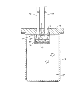
W ~ 98~1~236 PCT~US97/15460 DESCRIPTION OF DRAWINGS
FIGURE 1 is a schematic side view of a thin film bridge (TFB) pyrotechnic
pressure cartridge including a header assembly, manufactured in accordance
with the invention technique, reference FIG. 4 below. FIGURE lA schematically
5 depicts an enabling circuit therefor.
FIGURE 2 is an expanded cross-section of the thin film resistive element,
herein.
FIGURE 3 is an expanded cross-section of a prior art, generic
Semiconductor Bridge (SCB).
FIGURE 4 is a top view of the attachment of the thin film resistive
element/resistor chip to the header assembly.
FIGURE 5 is a schematic side view of a TFB similar to FIG. 1 and showing
a coaxial header assembly modification.
DESCRIPTION OF PREFERRED EMBODIMENTS
FIGU~E 1 illustrates a film bridge, TFB, pyrotechnic pretensioner
cartridge with a positive, powder retention, mechanism 11, which in this
invention is a requirement for the successful and consistent transfer of initiation
stimulus from the thin film bridge to the pressed prime powder/explosive mix.
The prime/explosive mix 12 of this invention within the loaded header
'0 assembly 8 includes hydroborate based materials. Titanium Subhydride
Potassium Perchlorate (TiH 1.6~i KCIO~, Zirconium Potassium Perchlorate, and
any other material capable of initiation using heat conduction or transmission
can be used.
The positive retention mechanism 11 is thus a requirement for the
consistent transfer of initiation stimulus from the thin film bridge 1 to the pressed
powder/explosive mix 12. The positive retention/compressive forces come into
play as follows: the prime mix 12 is consolidated around the thin film bridge 1
SUBSTITUTE SHEET (RULE 26)
CA 02233636 l998-03-3l
W O 98/10236 PCT~US97/15460
and electrical conductors 10, shown as PINS A and B in FIG. lA. During various
environmental exposures, this consolidated prime mix tends to lift away from thethin film bridge, TFB, hence the need for a positive retention or constant
compressive force.
The compactor, which is required for this purpose, consists of a positive
retention device 13, a wavy washer sic, contained between auxiliary powder
plate 14 and compression plate 15. As was demonstrated in Experiments
Numbers 1 and 2 described hereinafter, any positive retention is ~l~ett~ d to
none, with the wavy washer compactor 13 providing the optimum compressive
force. The presence of a positive and continuous compressive force maintaining
intimate contact between the explosive mix and the resistive bridge element 1
accordingly ensures a highly reliable transfer of initiation energy and
reproducible firing characteristics.
The pyrotechnic pressure cartridge includes a loaded header assemblv 8,
through which pass conductive pins; see FIG. lA. Pins A and B therein ha~ e
contact with film resistance bridge, FRB 1, yielding a resistance of 1.80 - 2.40ohms. See also FIG. 4 illustratin~ the thin film resistive element 1 and header
assembly 8.
FIGURE 2 is an expanded cross-section of a typical film resisti~e element
FRB 1. The base substrate/ceramic wafer 2 is typically .025" thick fine or ultrafine A1203. The fir~t steF~ in productinn is the sputtering or thermal ~aporation
of the selected r~istive layer 1 to achie~e a sheet resisti~ity of 0.l to 20 ohm~ rer
square. Nichrome is thermall~ e~ aporated upon the substrate, Al2O3, 99.6"~.,
pure; whereas Tantalum Nitride, Ta2N, if alternately selected, is sputtered ontothe .025" thick alumina A12O~. During ~ither the sputtering or evaporation
process, a seed layer of pure gold 3, in the neighborhood of 0.6 to 200 micro-
inches is also similarly applied. The final layer of gold 4 or other suitable metal,
SlJt~:j 111 UTE SHE~ET (RULE 26)
CA 02233636 1998-03-31
WO 98,J~236 PCT/US97~15460
e.g. such as aluminum or platinum which enables a bonding with aluminum
wire 10, is then electroplated on, to a thickness desired to support extemal
aluminum pin/wire bonding. The plated substrate is then subjected to a series ofphotolithography and etching steps to remove the unwanted material, yielding a
wafer of completed resistive elements, which can then be diced up, attached and
wirebonded to a suitable header assembly 8 such as appears in FIG. 4.
Significantly, these header assemblies may vary in diameter to accommodate a
variety of applications.
FIGURE 3 is an expanded cross-section of a typical, prior art,
Semiconductor Bridge (SCB). The starting material for the SCB manufacturing
process consists of a thin, intrinsic silicon film 5, in the neighborhood of 2
micrometers thick, that has been epitaxially grown on either a sapphire 6 or
single crystal silicon wafer approximately 500 micrometers thick. The first stepin the fabrication of an SCB consists of uniformly doping the thin silicon film 5 to
obtain the desired conductivity, resistance. The doping process typically consists
of diffusing varying impurities at some high temperature, followed by either
sputtering or evaporating the bonding layer 7, typically aluminum, onto the
previously doped silicon film 5. The wafer then is subjected to a series of
photolithography and etching steps to remove the unwanted material, yielding a
wafer of completed Semiconductor Bridges, which can be diced up, attacned and
wirebonded to the next higher assembly. A major disadvantage of this
technology is the wide variation in resistance values that occurs during heating.
The bridge resistance will typically double from its initial value, then drop tonearly one half its initial value as the melting point of the bridge is reached.In contrast, the selective Nichrome and Tantalum Nitride thin film bridges
herein have extremely stable resistances when heated. Likewise, multiple units
SUBSTITUTESHEET(RULE26)
CA 02233636 1998-03-31
W O 98/10236 PCTnUS97/15460
may easily be fired ~rom a commc~n ener~y source with the overall resistive loadbeing easily predicted at any instant.
FIGURE 4 depicts the resisLiv~ thin film att~t hm~nt 1 to the surface of the
header assembly 8 by way of either epoxy 9 or eutectic means. The wires 10 used
to connect ~e ~in fi~n bridge are either single or multiple 0.001 to 0.020 inch
diameter, aluminum. The plef~led method of their attachment to the substrate
is by way of ultrasonic wire bonding. It is critical to this invention that the wire
bonding be at a temperature low enough to prevent the formation of
interrnetallic voiding, hence weakening the bond to substrate pad interface.
FIGURE 5 depicts a coaxial modification of header assembly 8, described
~bove and illustrated in FIG. 1. Through the metal header 8, the right most
electrical conductor PIN A is shown to be ~rounded, the same being embedded,
at its confined end, in a dielectric, viz, glass.
The following experiments have been performed according to the
~le~ d description of this invention:
EXPERIMENT NO. 1
An experiment was performed to demonstrate the effects of various
positive retention mechanisms, including a silicone rubber compression pad,
magnesium dimpled closure, and a wavy washer concept. Several groups of
pressure cartridges were manufactured with the previously mentioned poslhve
retention concepts, and subjected to 200 cycles of temperature shock between -12C and +90 C. Listed below are the thin film bridge burnout times for these
confi~urations.
CONFIGURATION AVERAGE BURNOUT AVERAGE BURNOUT
40 C +9~ C
No Positive Retention 75 rnicroseconds~ 67 microseconds~ -
S;1 icone Rubber Pad 51 microseconds 59 microseconds
- 10-
SUBSTITUTE SHEET (RULE 26~
CA 02233636 1998-03-31
WO 98110236 PCT~lJS97/1~460
Dirr~le Closure 52 microseconds 43 rnicroseconas
Wavy Washer 48 microseconds 47 microseconds
Experienced failures to initiate.
EXPERIMENT NO. 2
A second experiment was conducted similar to Experiment No. 1 except th~t the
therrnal exposure consisted of 25 cycles of temperature shock between -6~- C and + 1''5
C. The results are as listed below.
CONFIGURATION AVERAGE BURNOUT AVERAGE BURNOUT
40 C +95 C
No Positive Retention 74 microseconds~ 66 microseconds"
Silicone Rubber Pad 56 microseconds 58 microseconds
Dimyle Closure 48 microseconds 41 microseconds
Wavy Washer 46 microseconds 43 microseconds
~ Experienced failures to initiate.
Testing indicated that without a positive retention mechanism in place, the
function times, as determined by bridge burnout, are approximately 50',o longer and
failure to initiate may occur.
SUPPLEMENTAL EXPERIMENTS
Several additional experiments have been conducted with Thin Film Bridges,
20 TFB, both with Nichrome and Tantalum Nitride resistive elements, and v ariousSemiconductor Bridges (SCB), all in the 2 ohm nominal range The SCB, using
phosphorous as the dopant, were evaluated on both sapphire and silicon substrates,
and had bridge geometries tailored for ESD robustness. The results are as listed belc)w,
along with a comparison in some cases of typical hot wire devices currently
25 commercially available.
8RIDGE FUNCllON ENERGY ESD ESD
CONFIGURATION TIME CONSUMED ROBUSTNESS ROBUSTNESS
/mi~roseconds)Imill~oul~c)RRGIMEN IA .REGIMEN 7R
SCB Savvhire Substrate 52 0.80 Passed Failed
30 SCB Silicon Substrate 50 0.90 Failed Not Tested
SU~S 111 ~JTE SHEET (RULE 26)
CA 02233636 1998-03-31
W O 98110236 PCTAUS97/15460
Nichro~eT~ 50 0.62 p~cc~d rassed
T~ lum NitndeTFB 41 0.60 r~CC~d ~assed
Ho~ireDevice 400 S-6 r~ d Passed
Regimen lA denotes a 500 picofarad capacitor charged to ~ kV, then discharged
S through a 5K ohm resistor into the test specimen. The discharge switch is defined as
two approaching metal spheres.
Regimen 2B denotes a 150 picofarad capacitor charged to 8 kV, then discharged
through a 330 ohm resistor into the test specimen, ~ ith a similar discharge su itch.
Many modifications and variations of this invention are possible in light ot
10 the above teachings. For example, the utility of the invention described herein
extends (in addition to automotive safety svstems) to commercial aircraft as ~ell
as commercial blasting and oil well usage wherein reduced energy, smaller
firesets and both repeatable and fast function times are sought. We therefore
intend the above terminology to illustratively describe the in~ention's preferred
15 embodiment and not to limit its scope. Within the scope of the appended claims,
in which reference numerals are merely for convenience and are not limiting, onemay practice the invention other than as the above specification describes.
The scope of invention is thus defined in the following claims, wherein
we claim.
- 12-
S~S 1 1 1 ~JTE SI IEET (RULE 26)