Note: Descriptions are shown in the official language in which they were submitted.
CA 0223367l l998-04-0l
WO97/12757 PCT~S96/15358
METHOD FOR PRES~K-vlN-~ PRECISION EDGES
USING DIAMOND-LIKE NANOCOMPOSITE FILM
FIELD OF THE lNV~N-llON
The present invention relates to erosion
resistant coatings, and especially precision-edge
preserving coatings made from diamond-like materials used
to keep substrate edges precise and sharp.
BACKGROUND OF THE INVENTION
The preservation o~ sharp edges is important
~or many products and industries. Many bladed industrial
and medical tools are only useful i~ they can have sharp
edges which can be maintained for reasonably long periods
of time. The sharpness which an edge has is the result
of the precision of the edge formed by the substrate and
any coatings thereon. Razor blades, for example, have an
edge ~ormed by producing a radius o~ curvature at the
blade's extreme tip o~ from about 75 to about 1000
angstroms. For comparison purposes, a human hair has a
width of about 100 micrometers. Such delicate precision
substrate edges are often coated to preserve the
precision o~ the edge for longer durations by attempting
to inhibit the degradation o~ the edge.
Precision edge degradation can be caused by
corrosive and/or erosive forces. Razor blades, for
example dull quite easily; to an extent, immediately upon
~irst use. Steel used ~or razor blades is there~ore
o~ten coated ~irst with a sputtered metal coating,
SUBSTITUTE SHEET (RULE 26)
CA 02233671 1998-04-01
WO97/12757 PCT~S96/15358
~ollowed by a coating of polytetrafluoroethylene (PTFE).
While the PTFE coating is usually tens to thousands of
angstroms thick, it appears to be substantially removed
~rom the blade upon first use. Enough PTFE seems to
survive to provide a measure of continued lubrication.
However, the PTFE coatings do not appear to prevent the
degradation of the precision edge.
Dulling of precision edges may be due to an
increase in the radius of curvature at the blade's
extreme tip, cracks, chips or breaks at the edge causing
a jagged edge, erosion of edge material, or a combination
of these ~actors. For razor blades, the degradation of
the precision edge causes increased friction leading to
user discomfort. Eventually the blade is replaced, or if
a part of a disposable implement, the entire razor is
simply discarded. For more expensive cutting implements
in industrial or medical fields, etc., the dulling o~
precision-edged tools results in the need for sharpening
or re-edging which takes time, requires the purchase of
replacement equipment, and increases costs.
The depositing of harder material coatings has
been tried in an attempt to preserve edge integrity. For
many applications, the coating should also have excellent
thermal stability; i.e. be able to withstand extreme
heat, as from use itself (saw blade) or ~rom
sterilization procedures (autoclaving surgical tools).
Metal-based coatings such as steel, zinc,
aluminum, chromium, nickel, alloys, cadmium, tantalum,
palladium, boron, silicon, copper, gallium, rhenium,
alloys thereof, etc. have demonstrated precision edge
preservation and are used in many industries to provide
SUBSTITUTE SHEEr (RULE 26)
CA 02233671 1998-04-01
WO97/12757 PCT~S96/15358
-- 3
protective coatings for sharp edges. However, coatings
made ~rom these materials are generally suitable only for
metallic substrates.
~ 5 Silicate based coatings are known to be
resistant to air, acid, alkali, and gases at elevated
temperatures. However, coatings made ~rom silicates are
not particularly strong materials and would not provide
appropriate protection for precision edges.
Certain ceramic materials used as coatings have
displayed good corrosion resistance and could conceivably
be used as edge preserving coatings. However, ceramics
are brittle and subject to thermal shock ~ailure. They
are typically and rough and porous and would not provide
the desired low friction.
Certain hard diamond-like coatings (DLCs), have
been tried. However, a coating must not only be hard,
but must have excellent adherence to the substrate being
coated. Known DLCs o~ten re~uire an interlayer to
adequately adhere them to a substrate. Ordinarily the
presence o~ such an interlayer may not pose a problem.
However, to preserve a precision edge, the total
thickness o~ all deposited coatings must not appreciably
increase the radius o~ curvature at the extreme tip o~
the edge which is very small. Further, the additional
process of depositing interlayers between the DLC and the
substrate increases the production cost. This can be
signi~icant, and even economically unsound ~or low cost
items, such as disposable razors and disposable razor
~ blades.
SUBSTITUTE SHEET (RULE 26)
CA 02233671 1998-04-01
wo97/l27s7 PCT~S96/15358
There~ore, a strong, hard, highly adherent,
temperature, pH and chemical insensitive coating that can
be applied to both metal and non-metal sur~aces to
preserve precision edges without applying interlayers,
would be highly desirable.
SUMMARY OF THE I~v~NllON
The present invention is directed to precision
edge-preserving, corrosion and erosion resistant coatings
made ~rom a class o~ diamond-like materials, and
substrates coated therewith. The diamond-like
nanocomposite materials can be "tuned" or predictably and
desirably altered by manipulating the chemical
composition, to result in the best combination o~
properties, o~ering maximum edge preservation protection
to the coated substrates.
In one embodiment, the present invention
relates to a method ~or preserving precision edges o~ a
precision-edged substrate, particularly a sharp-edged
substrate, by providing a substrate to be coated and
applying to the substrate a coating made ~rom a class of
diamond-like materials. The coatings are ~ormed ~rom
interpenetrating networks comprising a ~irst network o~
carbon in a diamond-like carbon network stabilized by
hydrogen, a silicon network stabilized by oxygen and,
optionally, at least one network o~ dopant elements, or
dopant compounds containing elements ~rom Groups l-7b and
8 of the periodic table.
A still ~urther embodiment o~ the present
invention relates to a precision-edged apparatus
SUBSTITUTE SHEEr (RIJLE 26)
CA 02233671 1998-04-01
WO97/12757 PCT~S96/15358
comprising a precision-edged substrate coated with a
precision edge-preserving coating. The coating applied
to the substrate is made ~rom a class o~ diamond-like
material having interpenetrating atomic scale networks o~
carbon in a diamond-llke carbon network stabilized by
hydrogen, a glass-like silicon network stabilized by
oxygen, and optionally at least one additional network o~
dopant elements or compounds containing elements,selected
~rom the group consisting of elements from Groups 1-7b
and 8 o~ the periodic table.
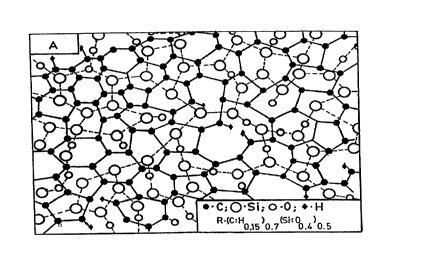
BRIEF DESCRIPTIO~ OF THE DRAWINGS
FIG. l is a schematic diagram showing the
principle microstructure o~ two-network (A), intermediate
(B), and three-network (C) nanocomposites.
FIG. 2 is a schematic diagram detailing the
main method o~ ~abrication o~ the DLN coatings.
FIG. 3 is a schematic diagram detailing the
methods o~ ~abrication o~ DLN coatings using re~lected
beam flow.
_ =
FIG 4 is a schematic diagram detailing a
pre~erred DLN ~abrication and deposition chamber.
FIG. 5 is an enlarged cross-section view o~ a
razor blade coated wlth th~ DLN coating.
FIG 6 is an enlarged cross-section view o~ a
razor blade coated with the DLN coating and an
interlayer.
SUBSTITUTE SHEET (RULE 26)
CA 02233671 1998-04-01
WO97/12757 PCT~S96/15358
-- 6
FIG. 7 is perspective view of a razor having
DLN-coated razor blades incorporated into the head.
FIG. 8 is a graph of plotted values of the
force required to make cuts in the wool felt cut test
versus the number of cuts for chromium and DLN coated
blades.
DET~TT~n DESCRIPTION OF THE lNVl~;NllON
The present invention is directed to precision
edge-preserving, corrosion and erosion resistant coatings
made from a class of diamond-like materials and
substrates coated therewith. The diamond-like materials
can be "tuned" or predictably and desirably altered by
manipulating the amounts of substituent to result in the
best combination of properties to offer maximum edge
preservation protection to the precision-edged
substrates.
In one embodiment, the present invention
relates to a method for preserving precision edges of a
substrate, particularly a sharp-edged substrate, by
applying to the substrate a coating made from a class of
diamond-like materials. The coatings are formed from
interpenetrating networks comprising a first network of
carbon in a diamond-like carbon network stabilized by
hydrogen, a silicon network stabilized by oxygen and,
optionally, at least one network of dopant elements, or
dopant compounds containing elements from Groups 1-7b and
8 of the periodic table.
SUBSTITUTE SHEEl- ~ULE 26)
CA 02233671 1998-04-01
WO97/12757 PCT~S96/15358
-- 7
For the purposes of this application, a
precision edge is understood to be the area of ultimate
narrowing of a substrate, resulting in the convergence of
two sides of the substrate to achieve a small radius of
curvature at a tip. A small radius o~ curvature is
understood to be one of from about 25 angstroms up to
several microns. For very sharp blades, the radius of
curvature is from about 75 angstroms to about lO00
angstroms. For other less~sharp cutting tools, the
radius at the tip may be up to hundreds of microns, while
still being considered a precision edge.
Corrosion is defined as the electrochemical
degradation of metals or alloys due to reaction with
their environment, which is accelerated by the presence
of acids or bases. In general, the corrodibility o~ a
metal or alloy depends upon its position in the activity
series. Corrosion products often take the ~orm of
metallic oxides or halides. In addition, corrosion may
be considered to be the degradation of non-metal
substrates by exposure to natural environmental
conditions as well as exposure to organic materials.
In addition to the edge-preserving and
corrosion-resistant properties of the coatings of the
present invention, the coatings are strong and erosion
resistant, such as to chemicals, abrasion, or ablation
while also being highly thermally stable. The coatings
would there~ore be impervious to biological or chemical
attack. The resistance of the coatings of the present
invention to erosion, reduces the possibility of, for
- example, physical chipping- This results in the surface
o~ the ~ubstrate being less likely to exposure to
~ environmental corrosive forces. The coatings have
SUBSTITUTE SHEET (RULE 26)
CA 02233671 1998-04-01
WO 97/12757 PCT/US96/15358
-- 8
excellent adherence to various substrates and are
resistant to thermal shock at elevated temperatures
beyond those known to erode known diamond-like coatings.
In one embodiment, Fig. 5 shows an enlarged
cross-sectional view of a razor blade 18 with a
precision-edged tip 24 coated with the DLN coating of the
present lnvention. In Fig. 5, a substrate 20 is coated
with a layer of DLN 21. A thin coating of
lO polytetrafluoroethylene (PTFE) 22 is shown deposited on
the DLN coating 21.
Fig. 6 shows a coated blade l9 with a
precision-edged tip 24 comprising a substrate 20 that has
15 been coated with an interlayer 23. The interlayer 23 is
then coated wlth the DLN coating 21, which is finally
coated with the PTFE coating 22. The interlayer is a
thin layer of material selected ~rom silicon, silicon
carbide, vanadium, tantalum, niobium, molybdenum and
20 alloys thereof, alone or in combination with one another.
The interlayers are deposited to a thickness of from
about 50 to about 500 angstroms. The PTFE is deposited
to a thickness of from about lO angstroms to about lO00
angstroms, preferably from about 25 to about 75
25 angstroms.
In one embodiment, the blades may be assembled
into a razor. Fig. 7 shows the blades 18 of Fig. 5
engaged in the head assembly 26 of a disposable razor 25.
30 An opening 27 in the head allows debris to pass from the
shaving plane. It is therefore understood that the DLN
coated blades of the present invention may be
manufactured as blades, such as replacement double-edged
SUBSTITUTE SHEET (RULE 26)
CA 0223367l l998-04-Ol
WO 97/12757 PCT/US96/15358
g _ , .
or single-edged blade, or may be incorporated into razor
assemblies.
The ~undamental structure o~ the preferred
5 corrosion and erosion resistant atomic scale diamond-like
nanocomposites (DLNs) used to coat the selected
substrates is comprised o~ two or more selE-stabilized
random networks, each stabilized chemically by additional
atomic species, while both networks also structurally
10 stabilize each other. An example o~ a material with such
a structure is the diamond-like nanocomposite (DLN) which
is the subject o~ U.S. Patent No. 5,352,493 and U.S.
Serial No. 08/249,167 ~iled May 24, 1994.
In the DLN, a random carbon network, mainly in
the ~orm o~ Sp3 bonded carbon ls chemically stabilized by
hydrogen atoms, and a glass-like silicon network is
chemically stabilized by oxygen atoms, resulting in a
purely amorphous structure. "Amorphous" as used herein
20 re~ers to a random structure or arrangement o:E atoms in a
solid state that results in no long range regular
ordering, and no crystallinity or granularity. The DLN
materials have an amorphous structure and do not contain
clusters greater than 10 Angstroms. This absence o:E
25 clusters at the atomic scale is a characteristic o~ the
DLN coatings o:E the present lnvention. Clusters can
destroy amorphous nature o~ the structure, and can serve
as active centers oi~ degradation. Cluster ~ormation is
prevented in the sources, in the primary plasma, in the
30 chamber space, and during Eilm growth.
- The atomic structure o~ the class oE diamond-
like nanocomposite (DLN) ma~erials o~ the present
- invention is shown in FIG. l(A). The materials may have
SUBSTITUTE SHEET (RULE 26)
CA 02233671 1998-04-01
WO97/12757 PCT~S96/15358
- 10 -
one or more separate disordered networks of dopants, as
shown in FIG. l(B) and l(C). The dopants may be any one
or a combination of the transition metals and non-metals
of the Groups l-7b and 8 of the periodic table, and all
three types of networks (C-H; Si-O and the dopant
network, Me-Me) bonded to each other predominantly by
weak chemical bonds. The network elements other than the
C-H network may be re~erred to as alloying elements.
Further, silicon and oxygen atoms may also be used in the
dopant networks with other elements and compounds.
The DLN coatings of the present invention may
comprise a two component network: the diamond-like
carbon-hydrogen network interpenetrated with the glass-
like silicon-oxygen network. A three component network
may also be used comprising the Si-O and C-H networks
with one or more dopant networks, with the dopants being
interspersed with the previously mentioned two
interpenetrating networks. In this instance three or
more interpenetrating networks will be present in the DLN
to form a so-called Me-DLN (metal-diamond-like
nanocomposite) network. It is understood that non-metal
dopant networks, may be incorporated as the optionally
present dopant networks interpenetrating the C-H and Si-O
networks.
The three networks (C-H matrix, si-o matrix and
a dopant matrix) are bonded to one another mainly by weak
chemical bonds. Carbide formation can be prevented even
at metal concentrations as high as 50~ (verified using
Auger electron spectroscopy, electron spectroscopy for
chemical analysis (ESCA), extended x-ray absorption fine
structure spectroscopy (EXAFS) and Fourier transform
infrared spectroscopy (FTIR)). Again, the properties o~
SUBSTITUTE SHEET (R~ILE 26)
CA 0223367l l998-04-Ol
WO97/12757 PCT~S96/15358
these materials can be varied over wide ranges depending
on the dopant and the concentration selected, as well as
- the deposition technique and parameters. As already
mentioned, the structure of these composites can be
tailored at the molecular level. There~ore, unique
electrical, optical, and other desirable solid state
properties with desired mechanical strength, hardness and
chemical resistance can be imparted on the DLN coatings.
Pre~erred dopant elements to be used in the Me-
DLN network, and which are particularly e~fective ~or use
as dopants in a corrosion-resistant Me-DLN coating are B,
Si, Ge, Te, O, Mo, W, Ta, Nb, Pd, Ir, Pt, V, Fe, Co, Mg,
Mn, Ni, Ti, Zr, Cr, Re, H~, Cu, Al, N, Ag and Au; with W,
Cr, Zr, Ti and H~ being pre~erred. Pre~erred compounds
which may be used as dopants include TiN, BN, AlN, ZrN
and CrN; with TiN and ZrN being most pre~erred.
The carbon content in the diamond-like
nanocomposite is greater than about 40 atomic ~ o~ the
DLN, pre~erably ~rom about 40 to about 98 atomic ~, more
pre~erably ~rom about 50 to about 98 atomic ~. Although
the DLN may theoretically be prepared without any
hydrogen, the hydrogen content is preferably at least
about l atomic ~ and up to about 40 atomic ~ o~ the
carbon concentration. The sum o~ the silicon, oxygen and
dopant elements and dopant containing compounds is
greater than about 2 atomic ~ o~ the DLN. In one
pre~erred embodiment, the ratio o~ carbon to silicon
atoms is ~rom about 2:l to about 8:l, hydrogen to carbon
atoms is about O.Ol:l to about 0.4:l, silicon to oxygen
atoms is about 0.5:l to about 3:l, and dopant to carbon
atoms is about O:l to about l.5:l. There~ore, in the DLN
network, ~or every l part carbon, there is ~rom about
SUBSTITUTE SHEET (RULE 26)
CA 0223367l l998-04-Ol
WO97/12757 PCT~S96/lS358
- 12 -
0.01 to about 0.4 parts hydrogen, ~rom about 0.125 to
about 0.5 parts silicon, and from about 0.0375 to about
1.0 parts oxygen. In such a scheme, i~ a third dopant
network were present, ~or every 1 part carbon, there
would be ~rom about O.Q1 to about 1.5 parts dopants
depending upon the desired characteristics to be imparted
to the Me-DLN network.
The low intrinsic stress ~ound in the DLNs
contributes to their corrosion resistance properties. A
coating must not only be unreactive to a corrosive agent,
but should also act as a barrier layer, preventing
contact between the corrosive agent and the protected
substrate. DLC ~ilms typically possess high intrlnsic
stresses, and as a result usually su~er ~rom pin holes
and overall porosity. Due to the comparatively low
stress present in DLN ~ilms and coatings, these coatings
are pore-~ree, and there~ore resist chemical attack and
permeation.
The presence o~ the glass-like silicon network,
stabilized by oxygen, serves to prevent the growth o~
graphitic carbon at high temperatures, to prevent metal
cluster ~ormation in metal-containing three-network
nanocomposites, and reduce the internal stress in the
nanocomposite structure and thereby enhance the adhesion
to substrates. This appears to lead to superior
adherence o~ the DLNs o~ the present invention to the
substrate material.
As already mentioned, to improve adherence o~
coatings, DLC coatings o~ten require an intermediate
layer between the substrate and the DLC coating. O~ten,
i~ the DLC coatings are too thick, delamination occurs.
SUBSTITUTE SHEEr (RULE 26)
CA 02233671 1998-04-01
Wo 97/12757 PCT/US96/15358
- 13 -
Surprisingly, with the DLN coatings of the present
invention, adherence is so good that an interlayer is
usually not required. As a result, the DLN coating may
be applied directly to the substrate, and more thickly,
5 without risking delamination from the substrate. The
ability to apply a thicker layer of DLN coating results
from the low intrinsic stresg due to the Si-0 network,
and is believed to contribute to the superior erosion
resistance of the DLN-coated substrates. Of course,
lO interlayers may be used with the DLNs if desired. The
tunability of the DLN structure also insures good
adherence o~ the DLN to the interlayer as the DLN may be
doped with a dopant to optimize compatibility and
adherence to the interlayer as well as to the substrate.
15 Such "tuning" is accomplished by incrementally altering
the particular dopant as well as the dopant
concentration. The DLNs may also have their properties
altered when no dopants are included. In addition to
altering chemical composition, changes in properties in
20 the two-network DLN system also can be achieved by
altering the deposition conditions in terms of
temperature and pressure, et~- The DLNs theref~ore adhere
well to both metal-containing and non-metal containing
substrates.
The DLNs of the present invention have
temperature stability far exceeding that of traditional
diamond-like (DLC) materials. Crystalline diamond is
stable to approximately llO~Q~C, upon which graphitization
30 occurs. Quartz has long term thermal stability to 1470~C,
and short term thermal stability up to 1700~C.
Traditional, non-alloyed diamond-like (DLC) films are
stable only to about 600~C before graphitizatiOn occurs.
- By contrast, the DLN structures used to provide the
SIJBSTITUTE SHEEl- (RULE 26)
CA 02233671 1998-04-01
WO97/12757 PCT~S96/15358
- 14 -
corrosion and erosion resistant coatings of the present
invention have long term stability to 1250~C and short
term stabillty to 2000~C. Therefore the thermal stability
of the DLNs exceeds that of DLCs while preserving the
amorphous, diamond-like state.
Further, in the range of from about 600~C to
about 1000~C, the chemical bonds of the carbon matrix of
DLN materials partly change from Sp3 to sp2. However, the
general structure of the nanocomposite and their
"diamond-like" properties are preserved. By contrast,
under similar conditions, the usual "diamond-like" carbon
(DLC) is graphitized and loses its diamond-like
properties. In the range of from 400~C to 500~C
(preferably 430~C), a reverse transition is observed,
whereby the ratio of Sp3 to sp2 is increased. It is
believed that a varying percentage of the carbon in the
DLNs is Sp3 bonded carbon.
The density of the C-H and Si-O two network DLN
varies from about l.8 to about 2.l g/cm3. The rest of the
space is taken up by a random network of nanopores with
diameters varying from about 0.28 to about 0.35 nm. The
nanopore network does not form clusters or micropores.
The properties of the two network DLN may then be
tailored by adding dopant. The dopants fill the nanopore
network in a random fashion, eventually resulting, at a
certain dopant concentration, in an additional network
without clusters or microcrystalline grains, even at
concentrations as high as 50 atomic ~. At concentrations
below about lO atomic ~, the dopants are distributed as
separate atoms in the nanopores of the diamond-like
matrix. The average distance between dopant atoms in
this quasi-random structure can be controlled by the
SUBSTITUTE SHEET (RULE 26)
CA 02233671 1998-04-01
WO97/12757 PCT~S96/15358
- 15 -
concentration of the dopant. When the relative
concentration of the dopant element or compound reaches
- about 20-25 atomic ~, the dopants form the third (Me-Me)
network in the DLN structure as shown in FIG. l(C).
The electrical properties of the DLN structures
of the present invention can be continuously varied over
a wide magnitude (at least about 20 orders) from a highly
dielectric state to a highly conductive state while
preserving and improving the properties of the DLN state.
A transition to a superconducting state, with the absence
of electrical resistivity, is observed at low
temperatures for certain three-network nanocomposite
networks.
Another advantage of the DLNs of the present
invention is their relative hardness and durability. The
DLNs, especially the metal doped DLNs combine high
microhardness with high elasticity. The microhardness
values of the DLNs of the present invention range from
about 5 to about 30 GPa.
The DLNs may be synthesized via co-deposition
by clusterless beams of ions, atoms or radicals of the
relevant elements, where the mean free path of each
particle species exceeds the distance between its source
and the growing particle film surface, and each beam
contains particles of well-defined energy. Carbon-
containing particle beams can be produced by plasma
discharge in a plasmatron and extracted as charged
particles by a high-voltage ~ield in a vacuum chamber and
~ directed onto the substrate.
SUBSTITUTE SHEEI (RULE 26)
CA 0223367l l998-04-Ol
WO97/12757 PCT~S96/15358
- 16 -
Figure 2 shows one pre~erred embodiment of the
coating chamber used ~or the DLN coating deposition
process. A vacuum deposition chamber 1 is provided to
coat a substrate sample. A precursor inlet system 13,
comprises a metal tube and a porous ceramic material 3
through which a liquid precursor, pre~erably a
polysiloxane, is injected. The precursor inlet system 13
is shown incorporated into the chamber through the
chamber base plate 11. The thermocathode 2 comprises a
resistively heated thoriated tungsten ~ilament 4.
Substrates, 5 to be coated with DLN ~ilm are attached to
the substrate holder 6. The power supply 8 is used ~or
biasing the substrates (DC or RF). In practice the
system is "pumped down" using normal vacuum pump down
procedures. A gate valve (not shown) located~on port 7
is closed and the system is back~illed with dry air,
nitrogen or argon until the chamber reaches atmospheric
pressure. The door of the chamber, 9, is then opened and
substrate to be coated 5 are attached to the substrate
holder 6 using any o~ many possible methods (spring clip,
screw, clamp, etc.). Special ~ixtures may be required
~or substrates o~ special shapes. The substrate holder
is designed in a way that it will also hold a cylinder
sample (not shown), which, in operation, rotates both
about the axis o~ the central drive sha~t 10, and its own
axis which is perpendicular to 10. In this way, the axis
o~ the cylinder would be perpendicular to the axis o~ 10.
When the substrates, ~or example razor blades
either singly or in a stacked arrangement, are loaded,
the door o~ the chamber is closed, the chamber evacuated,
and the gate valve opened to bring system pressure down
to at least 10-5 to 10-6 Torr, which is the desired range
o~ system base pressure. When the above base pressure is
SUBSTITUTE SHEET (RIJLE 26)
CA 02233671 1998-04-01
WO 97/12757 PCT/US96/15358
-- 17
achieved, argon gas is introduced into the chamber via a
needle valve or mass flow controller, until the chamber
- pressure reaches approximately 5x10⁻⁵ to lx10-3 Torr,
preferably about 1-3x10⁻⁴ Torr. The filament current, the
~ 5 filament bias and the electromagnet power supply are then
switched on. The filament current is the current that
passes through the thermocathode (also called the
filament or the cathode). The filament bias i5 the
constant floating voltage applied to the filament
(approximately -150V in relatlon to ground). Plasma
current is measured as the current between the filament
and the base plate or ground. This voltage provides the
field that moves electrons emitted by the filament to the
base plate 11. The electromagnet power supply provides
current to the electromagnet, which creates a magnetic
field that results in the electron path becoming a
spiral, increasing the electron path length and improving
the probability of collisions between the electrons and
the vapor molecules created due to precursor evaporation.
The substrate bias power supply is concurrently switched
on.
Switching on these power supplies results in
creation of an argon plasma, which is used to clean the
substrates prior to deposition. After the required
duration of cleaning, the precursor supply is opened.
Precursor flow is controlled via a needle valve and
occurs due to the difference in pressure between the
chamber and the outside atmosphere. When precursor flow
and vaporization in the chamber has stabilized, the argon
gas flow is turned of:~. The ionized precursor vapors
- form a plasma, ions from which are accelerated towards
the substrate holder due to the substrate bias. Thus,
deposition of DL~ film onto the substrate occurs.
SUBSTITUTE SHEET (RULE 26)
CA 0223367l l998-04-Ol
WO 97/12757 PCT/US96/15358
-- 18
Co-deposition of a dopant material is carried
out as i~ollows. Argon flow to the magnetron is commenced
and the magnetron 8 is switched on a~ter the base
pressure has been reached. A shutter 12 is used to
prevent deposition while the substrate is cleaned via
sputtering. When cleaning has been accomplished, the
shutter is opened and sputtering is carried out at the
desired power level. This may occur prior to commencement
o:E DLN ~ilm deposition, during DLN ~ilm deposition, a~ter
DLN Eilm deposition, or intermittently during DLN Eilm
deposition, depending on what kind oi~ ~ilm structure and
composition to be deposited are desired. Using DC or RF
sputtering, materials o~ all kinds (metals, ceramics,
alloys, etc.) can be used i~or co-deposition.
The growth conditions i~or nanocomposite ~ilms
are as follows, with re:Eerence to FIG. 2. The pressure in
the deposition chamber 1 should not exceed 10-3
torr, with the pressure in the active zone of the plasma
generation 2, in the range ~rom about 1.0 x 10⁻³ to about
5.0 x 10⁻² torr. The temperature o:E the substrate should
not exceed about 200~C with the temperature of the cathode
~ilaments being in the range ~rom about 2100 to about
2950~C. The current in the cathode i~ilament is ~rom about
70 to about 130 A, with the voltage across the ~ilament
being :Erom about 20 to about 30 V. The voltage with
respect to the ground is from about 70 to about 130 V
with the plasma current being i~rom about 0.5 to about
20.0 A. The voltage o~ the substrate holder is i~rom
about 0.1 to about 5.0 Kv, with all the carbon-
containing and Si-containing species having kinetic
energy in the range o~ ~rom about 100 to about 1200 eV
and :Erom about 25 to about 300 eV respectively. The
metal beams consist o~ i~ree atoms or monatomic ions. The
SUBSTITUTE SHEET (RULE 26)
CA 0223367l l998-04-0l
W097/12757 PCT~S96/15358
-- 19 -- ,
kinetic energy of the metal atoms/ions does not exceed
~rom about 25eV. With a precursor ~low rate ~rom about
~ 0.5 to about 5.0 cc/hour, the growth rate o~ the DLN is
~rom about 0.1 to about 2.0 micrometers/hour.
The pre~erred range of operation ~or most
applications is a pressure of about 1-3x10-~ Torr, a
plasma current o~ about 1 amp., a filament current o~
~rom about 60 to about 75 amp., a substrate voltage o~
~rom about 600 to about 1000 V DC, or ~orward power of
about 100 W in RF mode. The pre~erred ~requency ~or RF
mode is ~rom about 90 to about 300 KHz. The pre~erred
magnetron power depends on the type of material,
composition and structure desired ~or the DLN coating.
In a ~urther pre~erred embodiment, a plasma
discharge in a triode plasmatron is used for DLN
deposition, as shown schematically in FIG. 3, with the
plasma energy density above about 5 Kwh/gram-atom o~
carbon. The charged particles are extracted by a high
voltage ~ield in the vacuum chamber and directed onto the
substrate. It is pre~erable that the potential o~ the
substrate holder is ~rom about -0.3 to about +5.0 Kv, and
most pre~erably 1.0 +/- 0.2 Kv for DC and RF. In the RF
mode, the ~requency is in the range o~ ~rom about 0 to
about 25 Mhz, and pre~erably ~rom about 90 to about 300
kHz ~or RF. The ratio o~ the electron emission to the
carbon precursor ~low in the plasmatron is ~rom about 0.5
to about 1.5 electrons per particle.
Organosilicon compounds, such as siloxane, are
preferred precursors ~or C, H, Si and O. One pre~erred
organosilicon compound is polyphenylmethylsiloxane,
containing 1 to 10 Si atoms. The high boiling point
SUBSTlTllTE SHEET (RULE 26)
CA 02233671 1998-04-01
WO97/12757 PCT~S96/15358
- 20 -
siloxanes may be introduced directly into the active
plasma region through a porous ceramic or metallo-ceramic
(3 in FIGS. 3 and 4) which is heated via radiation
thermocathodes 4. The photon and electron emission of
the thermocathodes affect the evaporation, fragmentation
and ionization of the precursor molecules on the surface
of the ceramic, which thereby functions as an ion source
for the plasma generator. An alternative method for
injection of the siloxane precursors is to use direct
injection ~rom a diffusion pump.
The formation of dopant-containing beams may be
realized by any one of, or combination o~, the following
methods: l) thermal evaporation; 2) ion-sputtering; 3)
ion beams. The dopant-containing beams are directed onto
the growing film surface through the vacuum chamber to
exclude interparticle collisions in the deposition
chamber itself. Substrates are placed in an adjacent
chamber on a rotating substrate holder, (for example a
drum) which ensures double rotary motion, said adjacent
chamber being connected to the plasma generation chamber
by an opening for the emission of the atomic or ionic
beams, as shown schematically in FIG. 3. Alternatively,
the plasma generation may be carried out within the
chamber containing the substrates (Fig. 2). A DC or a
radio frequency potential is generally applied to the
substrates during the deposition process. No external
substrate heating is required. The substrate holder may
be designed specifically to hold parts of different
shapes such as cylinders, as would be apparent to one
skilled in the field. Useful variation o~ the above
described methods ~or deposition of DLN films include the
use of sputtered silicon and oxygen gas as precursors for
the Si and ~2 ~ the use of sputtered carbon and hydrogen or
SUBSTITUTE SHEET (RU~E 26)
CA 0223367l l998-04-Ol
WO97/12757 PCT~S96/15358
- 21 -
hydrocarbon gas used as carbon and hydrogen precursors,
or any combinatlon thereof.
For deposition on non-conducting substrates,
such as plastic, a method whereby a flow of neutral
radicals is reflected from a high voltage target and
directed to the substrate as shown schematically in
FIG. 4. The process employs depositions similarly to
those shown in FIG. 3, except that a reflecting electrode
is used to generate a neutral beam. This process
eliminates surface damage of the substrate resulting from
charged and/or fast particles impinging on the substrate
during growth.
Extremely uniform and nonporous thin dielectric
films may be deposited according to the present
invention. The thickness of the deposited DLN coating
has no theoretical limit. Existing technology and
available equipment have allowed atomic-scale composite
films and coating thicknesses typically in the range from
about tens of angstroms up to 10 micrometers. The
thickness of DLN deposited to adequately protect a sharp
edge will depend upon the nature of the substrate. Very
small sharp blades may only require DLN coatings from
about 5 nanometers to about 150 nanometers, while other
apparatuses may require a protective DLN layer which is
several micrometers (microns) thick. Therefore, the
above-described DLN coatings of the present invention may
be deposited on the selected substrate, or on interlayers
i~ desired, in thicknesses ranging from about 5
nanometers to about 12 micrometers, preferably from about
- 20 nanometers to about 12 micrometers, depending only on
the desired application of the coated substrate.
SUBSTITUTE SHEET (RULE 26)
CA 02233671 1998-04-01
WO97/12757 PCT~S96/15358
- 22 -
The deposition may be tailored or "tuned" to
meet the properties required for a particular
application. The random interpenetrating of the two- or
three-network DLNs guarantees uniform strength of the
structures in all directions. The structures are free of
micropores even at thicknesses of about 80 Angstroms (8
nm). The DLNs are therefore extremely stable and possess
unique combinations of chemical, mechanical, electronic,
and superconducting properties.
Many uses for the precision edge-preserving DLN
coatings of the present invention exist, including but
not limited to the coating of metals and non-metals,
surgical instruments, razor blades, industrial and non-
industrial tools, cutlery, knives, pocket knives, and anyprecision-edged substrates which are vulnerable to
corrosive and/or erosive attack, and dulling. The
following examples serve only to further illustrate
aspects of the present invention and should not be
construed as limiting the invention.
EXAMPLE 1
Deposition of Undo~ed DLN Coatinqs on Razor Blades
One set of 2000 razor blades was coated on both
sides with undoped DLN. The razor blades were mounted on
a steel fixture with the blade edges facing the
deposition sources (the blades held parallel to the
beam). Deposition was carried out at a pressure of 1.1 x
10-4 Torr, a plasma current of 1.0-1.1 amp. and an RF load
power of 125W. The deposition took place ~or 30 minutes.
Shutters were used to shield the substrates during
SUBSTITUTE SHEEr (RIJLE 26)
CA 0223367l l998-04-Ol
WO97/12757 PCT~S96/15358
startup and shutdown of the plasmatron. At the
deposition rate o~ 0.7 micrometers/hr, the test run
resulted in a deposited DLN thickness o~ 3000 angstroms
(0.3 micrometers) on a blade sur~ace held ~lat ~acing the
deposition beam, and a 300 angstrom ~ilm on a sur~ace
held at a 10~ angle to the deposition beam. The thickness
on the ultimate blade tip was approximately 3000-5000
angstroms, which was too high, resulting a dulling of the
blade.
EXAMPLE 2
A second coating run nearly identical to that
described in Example 1 was conducted, except that the
test time was 10 minutes. The shorter test time resulted
in a deposited DLN coating thickness on the blade edges
o~ approximately 300-500 angstroms. The radius o~ the
blade tip a~ter coating was 200-300 angstroms.
EXAMPLE 3
De~osition o~ Poped DLN Coatinqs
Additional blades were coated with Zr-DLN and
W-DLN under the ~ollowing chamber conditions. RF bias
~requency was lO0-250 kHz, the load power was 80-120W,
~orward power was 100-150W, with the tungsten (W) and
zirconium (Zr) doping at ~rom about 10-20~.
SUBSTITUTE SHEEr (RULE 26)
CA 02233671 1998-04-01
WO 97/12757 PCT/US96/15358
EXAMPLE 4
Wool Felt Cuttinq Test
The blades coated according to the procedures
o~ Examples 1-3 were tested by applying the blades
against wool ~elt and cutting the ~elt 500 times. The
di~erence between the ~orce required to make the cut the
~irst and last (500th) time was determined. A lower
cu~ting ~orce was re~uired by the blades coated with the
DLN versus chromium coated blades having a PTFE layer o~ -
2000-3000 angstroms. See Figure 8.
EXA~qPLE 5
Mechanical Properties o~ DLN Films
High hardness and mechanical modulus
measurements were obtained on 9 di~ferent compositions o~
DLN and doped-DLN ~ilms. Measurements were carried out
using a nanoindenter (Nanoinstruments, Knoxville, TN).
Hardness ranged from about 6 to about 21 GPa. Elastic
25 modulus o~ ~rom about 60-220 GPa was achieved.
Hardness/modulus degradation in the ~ilms was mini~al
a~ter exposure to 500~C.
Many other modi~ications and variations o~ the
present invention are possible to the skilled
practitioner in the ~ield in light o~ the teachings
herein. It is there~ore understood that, within the
scope o~ the claims, the present invention can be
practiced other than as herein speci~ically described.
SUBSTITUTE SHEET (RULE 26)