Note: Descriptions are shown in the official language in which they were submitted.
CA 02233942 1998-04-03
W O 98/12670 PCT/CA97/00663
BlO~n~rRTC nDENT~CAl~ON SYSTEM FOR PROVnDnNG SECU~E ACCESS
Field of the Invention
This invention relates generally to personal identification systems and more
particularly relates to a biometric security identification system (BSIS).
Background of the Invention
Biometric security identification systems, such as fingerprint sc~nning and input
devices are becoming more commonplace as the need to validate authorized users of
computers, databases, and secure spaces grows. As computers become more mini~hlrized~ so
0 too are other cu~ u~lication and security devices decreasing in size. One of the more
important reasons~ however. to mini~tllrize electronic devices is to lessen the burden of
porting them.
The use of security systems is generally well Icnown. Their use is increasing with
s greater availability of digital electronic components at a relatively low cost. Such systems are
known for securing buildings, banks, automobiles, computers and many other devices. For
example, U.S. Pat. No. 4, 951, 249 discloses a computer security system which protects
computer software from unauthorized access by requiring the user to supply a name and a
password during the operating system loading procedure ("boot-up") of a personal computer
20 (PC). This is accomplished by the insertion of a special card into an input/output expansion
slot of the PC. During the loading of the operating system of the PC, the basic inputloutput
system (BIOS) scans memory addresses of the card for an identification code, consisting of a
55AA hex code. When this hex code is located, the BIOS instructions are vectored to the
address where the target hex code resides and instructions at the following addresses are
~5 executed as part of the initialization routines of the system boot-up procedure.
This PC security system, lltili7ing password protection, is typical of many systems
that are currently available. Password protection requires a user's narne and a password
associated with that user's name. Only once an associated password is detected for a valid
30 user's name does the PC complete the boot-up roL~ine. Though passwords may be useful in
some instances, they are inadequate in many respects. For exarnple, an unauthorized skilled
CA 02233942 1998-04-03
WO 98/12670 PCT/CA97/00663
user with a correct password in hand, can gain entry to such a processor based system. Yet
another undesirable feature of the foregoing system is that passwords on occasion are
forgotten, and furthermore, and more importantly, passwords have been known to be
decrypted.
s
As of late one of the most ubiquitous electronic components is the digital processor.
Multi-purpose and dedicated processors of various types control devices ranging from bank
machines, to cash registers and automobiles. With ever increasing use of these processor
based devices, there is greater concern that unauthorized use will become more prevalent.
o ~hus, the verification and/or authentication of authorized users of processor based systems is
a burgeoning industry.
Alarrns and security systems to warn of unauthorized use of automobiles and other
processor controlled systems are available, however, these security systems have been known
ls to be circumvented. Unfortunately, many commercially available solutions aimed at
preventing theft or unauthorized use of automobiles have also been circumvented. As of late,
initiatives have been underway in the security industry, to provide biometric input devices to
validate users of electronic and other systems, that are to have restricted access. One
limitation associated with many typical comrnercially available biometric systems is the large
~o physical size of the im~ging devices. Concern with placing a biometric input device in an
location that is ~rces~ihle to the public is the risk of the input device being v~n~l"li7Prl
In the field of digital and analog comm~mic~tions7 wireless devices are becomingmore commonplace. Inexpensive computer systems are currently commercially available
2s wherein printers communicate with computers which in turn communicate with other
c~ lpu~ , via infra red tr~n~mitters and receivers. Other devices, using other optical
co~ l.,ic~tion systems, such as data transmitting/receiving wrist watches are now available
in department stores at ~ .LallLially affordable prices; these wrist watches include processors
and software for c~ ,l,ullication with a colll~uL~:. and for downloa ling and uploading small
30 amounts of data as required.
CA 02233942 1998-04-03
W O 98/12670 PCT/CA97/00663
Ob~ect of the Invention
It is an object of this invention to provide a portable biometric input device for
sensing input biometric data, and transmitting the data to a receiver.
5 Summary of the Invention
In a first broad embodiment the invention seeks to provide a portable biometric input
device comprising: biometric sensing means for sensing biometric input information.
generating biometric data therefrom, and providing the biometric data in relation to the
lo sensed biometric input information; tr~n~mi~ion means for receiving at least an aspect of the
biometric data and for transmitting a signal in dependence upon the at least an aspect of the
biometric data; and a battery for providing power to the device.
In an embodiment, the transmission means is a wireless tr~ncmi~ion means for
5 transmitting a signal in dependence upon the at least an aspect of the biometric data.
In an embodiment. the tr:~n~ ion means comprises a biometric data encoder and aninfrared transmitter for transmitting a signal in dependence upon the at least an aspcct of the
biometric data.
In an embodiment. the device further comprises storage means for storing data related
to said biometric data.
In an embodiment, the device further comprises processor means for processing the
25 biometric data.
In an embodiment, the processor means is for comparing the biometric data with
previously stored biometric data to provide comparison results; and the signal in dependence
upon at least an aspect of the biometric data comprises a signa} in depen~l~nce upon the
30 comparison results.
CA 02233942 1998-04-03
W O98/12670 PCT/CA97/00663
In an embodiment, the device further comprises means to receive a password and
wherein the ~ c~iion means is for tr~n~mitting a signal in dependence upon at least an
aspect of the biometric data and the password.
In an embodiment, the device further comprises means to receive a password and
wherein the processor means is for co...l-~. ;.,g the biometric data with previously stored
biometric data and the password and a previously stored password to provide col~palison
results; and the signal in dependence upon at least an aspect of the biometric data comprises a
signal in dependence upon the co~ "~Qn results.
In an embodiment, the device fi~rther comprises means for encrypting at least anaspect the biometric data; and the tr~n~mi~ion means is for receiving the encrypted data and
for tr~n~mitting a signal in dependence upon the at least an aspect of the encrypted data.
In an embodiment, the means for encrypting the biometric data comprise
public/private key encryption means.
Alternatively, the means for encrypting the biometric data comprise session key
encryption means.
In an embodiment, the biometric input means is a fingerprint im~ging device.
In an embodiment, the device further comprises a housing in the form of a watch
r,~Pn~pnt and a watch face.
2s
In an embodiment, the biometric input means comprises associated electronic
Cil~;Ui~l,y and conductive pads disposed on the watch face.
In a further broad embodiment, the invention seeks to provide a portable biometric
input sensor comprising: an array of sense ~le1llPnte spaced apart and comprising a sensing
electrode for sensing biometric input; drive means coupled to at least some of the sense
CA 02233942 1998-04-03
W O9811267~ PCT/CA97100663
elements for controlling and addressing each of the at least some sense elements according to
a predetermined sequence, for receiving a signal in dependence upon the biometric input. and
for providing biometric data in dependence upon the sensed biometric input; processor means
for processing biometric data; and, wireless transmission means for transmitting to a receiver
s a signal that corresponds to at least an aspect of the biometric data.
In an embodiment~ the device further comprises means for encrypting the biometric
data further comprising means for encrypting at least an aspect the biometric data; and the
tr~n~mi~ion means is for receiving the encrypted data and for transmitting a signal in
I o dependence upon the at least an aspect of the encrypted data.
In an embodiment. the means for encrypting the biometric data comprise
public/private key encryption means.
In an embodiment, the means for encrypting the biometric data comprise session key
encryption means.
In another broad embodiment the invention seeks to provide a biometric security
identification system comprising: a portable transmitting module comprising a biometric
sensing means. means for encoding biometric data and wireless tr~n~mi~ion means for
tr~n~mit~in~ the encoded biometric data as an encoded signal; and a receiving module
comprising means for receiving the encoded signal, means for extracting the encoded
biometric data~ and means for comparing the encoded biometric data with predetermined
reference values, and means for authorizing access to a host system.
2s
In an embodiment, the biometric sensing means comprises a fingerprint scanner.
In an embodiment, the device further comprises means for encrypting the biometric
data further comprising means for encrypting at least an aspect the biometric data; the
- 30 tr~n~mi~.sion means is for receiving the encrypted data and for transmitting a signal in
dependence upon the at least an aspect of the encrypted data; and the means for extracting the
CA 02233942 1998-04-03
W O 98/12670 PC~/CA97/00663
encoded biometric data comprises means for decrypting and for extracting the encoded
biometric data.
In an embodiment, the means for encrypting the biometric data comprise
public/private key encryption means.
In an embodiment, the means for encrypting the biometric data comprise session key
encryption means.
o In yet another broad aspect, the invention seeks to provide a portable biometric input device
comprising: sensing means including a platen upon which to rest a finger, said sensing means
for sensing the presence and location of fingerprint ridges upon the device; processor means
for processing sensed data; and, wireless k~n~mi~ion means for transmitting a signal that
corresponds to at lcast an aspect of the sensed data; and a battery for providing power to the
1 5 device.
The advantages of a system in accordance with this invention are numerous For example,
providing a lightweight fingerprint input tr~n~ u~r capable of wireless communications with
a remote system obviates the requirement of securing the input tr~n~ducer from vandals and
prevents tampering therewith. Providing an input sensor that serves as a user's personalized
key, offers distinct and obvious advantages. Firstly, the sensor may be protected by the user,
being his or her own personal device. and furthermore, a user's personalized sensor may
comrnunicate with several different devices that require validation in the form of a users
biometric input data, for example, the input sensor may provide a valid access code in the
forrn of a biometric key, to unlock a locked car door, a house door, and/or to provide access
to a banking m~hin~ or a computer. Furthermore, a user's personal sensor can be
programmed with its own identification key which can accompany a user's biometric data in
t_e validation process, to validate both the sensor and the user.
Brief D~ "ion of the D. ~
Exemplary embodiments of the invention will now be discussed in conjunction withthe ~rh~ drawings in which:
CA 02233942 1998-04-03
W O 98/12670 PCT/CA97/00663
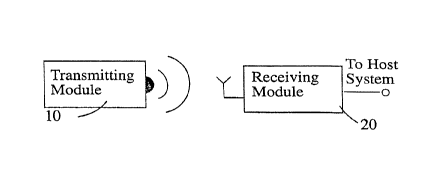
Fig. I is a block diagram of the biometric security identification system (BSIS)according to the invention;
Fig. 2 is a simplified diagram of a sensing device for use with the present invention
showing an array of sensing elements together with associated addressing circuitry;
Fig. 3 is a simplified diagram of a sensing element for use with the present invention;
Fig. 4 is a s~.h~m~tic diagram of an amplifier circuit for use with the present invention;
Fig. 5a is a digital watch according to the present invention;
Fig. ~b is an analogue watch according to the invention;
o Fig. 6 is a block diagram of the transmitting module of Fig. I;
Fig. 7 shows a block diagram of the receiving module of Fig. 1;
Fig. 8 is a flowchart for illustrating a mode of operation of an embodiment of a BSIS
according to the present invention;
Fig. 9 is a flowchart for illustrating a mode of operation of an cmbodiment of a BSIS
15 according to the present invention;
~ig. 10 is a flowchart for illustrating a mode of operation of an embodiment of a BSIS
according to the present invention further C~ illg bi-directional communication;Fig. 11 is a flowchart for illustrating a mode of operation of an embodiment of a BSIS
using bi-directional communication and a time out according to the present invention;
Fig. 12 is a biometric credit card according to the present invention;
Fig. 13 is a device according to the present invention incorporated into a keychain and
using infrared wireless communication; and
Fig. 14 is a device according to the present invention incorporated into a keychain and
using RF wireless commllnic~tion.
Detailed Description
Fig. I illustrates the block diagram of a biometric security identification system
(BSIS) according to the invention. The system comprises a transmitting module 10 and a
receiving module 20 connected over a tran~mic~ion channel in the form of a wireless
30 tr~n~mie~ion channel. The tr~n~mitting module 10 measures a biometric characteristic of a
person requesting access to a protected host system and converts the biometric characteristic
CA 02233942 l998-04-03
W 098/12670 PCT/CA97/00663
into a biometric ic~entifi~ti-)n (ID) code. The ll,.n~ r module is adapted to be carried or
worn by the user, and therefore can take any suitable form, such as a wrist watch, a badge, a
wallet, etc.
The biomekic information may be acco~ pallied by a password for increased security
of the identification process. In this way, access to the protected host system is denied to
unauthorized users, who may have a similar biometric ID. Similar biometric ID may occur if
the tr~n~inrer has a low sensitivity, for example for cost or/and mini~ ion reasons. The
password could be any m~rl~int? readable code like a PIN, an account number, or a time-
o varying code. Selected passwords can be unique to the watch itself, or they can be chosen by
the user.
It is apparent that various types of trz~n.~duçers may be used, such as image ort~ p~ Lulc~ t~n~iurers~ electromagnetic field sensors, optical sensors. etc. Preferably, the
sensitivity of the tr~n.~ rf r allows for capture of biometric data which reasonably
distinguishes the user. In an embodiment, the transmitting module is in the form of a wrist
watch provided with a fingerprint reader and described in more detail bclow.
The biometric ID is transmitted to receiving module 20, which is attached to a host
system. The tr~n~mi.~.~ion is preferably made by motlnl~ting an infrared (IR) carrier with the
biometric ID, but any other type of communication between the tr~n~mitting module 10 and
receiving module 20 may be used. Preferably wireless communication means are used as
dictated by selected design parameters, such as the tli~t~nre between the modules, the power
budget, etc. Preferably, and for obvious security reasons, a wireless communication means
employed should minimi7e the risk of interception and recording of a biometric ID.
At receiving module 20, the biometric ID is compared to a reference ID pre-stored in
a memory. If the current biometric ID (IDC) m~trhr$ a reference ID (IDREF3, access to the
host system is authorized. The host system could be a computer system, an ATM banking
machine, a door latch or any other system which must be secured against unauthorized
CA 02233942 1998-04-03
WO 98/12670 ~CT/CA97/00663
access. In an alternative embodiment, the biometric ID is compared in the transmitting
module 10 and an access code is sent to the receiving module 2~) for comparison.
Referring to Fig. 2. part of a sensing device for use in an embodiment of the present
5 invention and implemented on a semiconductor chip is shown comprising a single active
matrix addressed sensing pad 119 having an X-Y array of sense elements consisting of r rows
(1 to r) with c sensing elements 117 in each row. In practice there may be about 30Q rows and
200 columns of regularly-spaced elements occupying an area of approximately 2 cm x 3 cm.
This area is for accepting a fingertip for sçz~nning Should such a sensing pad 119 be made
lo larger~ it could be used for sc~nning other items such as a palm of a hand.
Sensor elements 117 are disposed in such a fashion that they are capable of
distinguishing the smallest desired feature of a fingerprint. Preferably, the placement and
spacing of the sensor elements allow an image of a fingerprint, once scanned, to contain all
5 required features for analysis. The sensing element 117 is smaller than half the smallest
sensible feature size allowing a suitable image to be generated. Empirical studies reveal that a
square plate of about 50 !lm edge length is suitable for fingerprint sensing. Although the
~al~lus is described with reference to an array of sensing elements 117 having substantially
square shape. it is possible to use different configurations of sensing elements 117 such as
20 concentric circles or a spiral and different shapes such as triangles, circles. or rectangles.
The array of sensing elements 117 is connected through an analog switch matrix to
facilitate reading the finge.y..lll image out of the sensing array 119. Timing and sequencing
logic 116 selects each element in the array in turn to produce a complete image of a
2s fingerprint presented to the device. The signal may be output directly as an analog signal or
may be converted to a digital signal prior to output from the device.
The sensing pad 119 further comprises a ground ring 115 and bonding pads 118
rlesigned for connection to other components or to p~ck~ging The ground ring 115 also
30 serves to provide a cornmon ground for the sensing pad. Accordingly, it is important that the
ground ring 115 and integrated circuit elements be designed so as to minimi7~ noise to each
CA 02233942 1998-04-03
WO98/12670 PCT/CA97/00663
sensing element 117. The signal to noise ratio that is acceptable will vary between
applications and should be adjusted to meet the needs of a specific design. When possible~
p~ck~ging should be selected to limit noise.
Referring to Fig. 3, a single sensing plate 120 is shown. Such a sensing plate 120 is
designed to be used in arrays and preferably is smaller than half the smallest sensible feature
size as indicated above. Charge sensing electrode 121 is connected to an active element which
is shown as a three terminal switching device in the form of a field effect transistor (FET)
having a source, a drain, and a gate 126. The gate 126 is connected to the sensing electrode
o 121 by an interconnect 124. Disposed bet.~,veen the gate 126 and the transistor 130 is a gate
oxide 127. Such transistor configuration is known in the art.
Above the charge sensing electrode 121 is disposed an overglass 122 which serves to
protect the charge sensing electrode 121 and to space the electrode and a fingertip presented
thereto. Below the charge sensing electrode 121 is disposed a field oxide 125. ~ finger placed
against the overglass 122 induces charge in the charge sensing electrode 121. By amplifying
the charges induced by a fingertip on the charge sensing electrode 121 with an amplifier
circuit such as is shown in Fig. 4, the inclllce~l charges can be rendered easily distinguishable.
Referring to Fig. 4, a sensing pad 120 is electrically grounded. A second side is
connected through electrostatic discharge protection 131 in the forrn of resistors and diodes.
A filter circuit 132 and 133 improves circuit operation. Transistors 134, 135, 136, and 137
provide amplification of inf~ ecl voltages allowing a signal at an output of transistor 136 to
be digitized by a low cost A/D COllV~:;lt~l.
Assuming that the charge density on the fingertip is ~h~ 11y even, induced
charges on the charge sensing electrode 121 will depend solely on the rliet:~nt~e between the
charge sensing electrode 121 and the skin of the fingertip inci~lcing the charge. Further, as the
induced charge falls off with the rli~t~nt~e, the closest skin of the fingertip will induce a larger
proportion of the charge. The sensor is employed in the above fashion to image fingertips.
CA 02233942 1998-04-03
W 098/1267~ PCT/CA97/00663
Referring to Fig. 5a, a watch is shown comprising (in part~ the present invention. The
watch 50 is secured in place on a person7s wrist for example by way of a strap 51. Alternative
methods such as a chain as is common in pocket watches, a pouch (not shown)~ velcro~ a pin,
or means for secllring the watch to a sporting apparatus may also be used. A time display
means 52 in the form of an LCD display, an LED display, an analogue time display~ a voice
generated time, or a Braille time display is disposed upon the watch 50 in a conventional
manner. Preferably, the time display means 52 is offset to allow for sufficient contiguous
surface area for a biometric sensor 53. Alternatively, the biometric sensor 53 is designed to be
superimposed upon the time display means 52 and not interfere therewith as shown in Fig.
o 5b. An emitter port in the form of an infra red emitter port 55 is located on the watch 50 such
that light emitted from the infra red port 55 is directed toward a sensor (not shown) in use. In
Fig. 5a and Fig. Sb, the infra red emitter port 55 is located on the top of the watch above the
face and pointing substantially coplanar to the watch face. In this orientation. an emitted
signal is directed away from the body of a user and forward during normal use.
The biometric sensor means 53 is of the form described above and shown in Figs. 27
3, and 4. Alternatively, the biometric sensor means 53 is a capacitive fingerprint scanner
requiring pre-charging as are well known in the art. Further alternatively, the biometric
sensing means 53 is an optical biometric sc~nning device in the forrn of a retinal scanner, an
~o optical fingerprint scanner, an optical palm scanner, or any other suitable (and portable)
biometric sensing device.
Referring to Fig. 5b, an analogue watch 150 is shown. ~nalogue watches of this type
are well known and are in common use. On to the face of the analogue watch 150 are
deposited a plurality of metal pads 155 and associated circuitry 156. The pads 155 and the
associated circuitry 156 act as sensors and addressing circuitry and combine to form the sense
electrode for a biometric input device. The analogue watch 150 is ~ ignPd to be easily read
in the presence of the pads 155 and the associated circuitry 156. This is accomplished by
ensuring that a short hand on the watch 150 is long enough to be partially visible at each
- 30 outside edge of the metal pads 150 in each possible orientation. Alternatively, this is
accomplished by ~lesigning the hands of the watch to be visible through or between the pads
Il
CA 02233942 1998-04-03
W 098/12670 PCT/CA97/00663
150. Further ~ltern:ltively, this is accomplished by ~le~igning the pads 150 such that
information on positions of the watch hands is transmitted through or by the metal pads 150.
Further alternatively, this is accomplished by ~lçcigning the watch face with an offset
analogue time indication providing sufficient space for the pads 150 as is shown in Fig. 5a.
The associated ci~ y 156 is coupled to driver and sensing circuitry for reading the
electrode in the form of metal pads 155 and for determining the presence of a fingerprint or
other biometric input. The analogue watch 150 also comprises an infra red emitter port 55.
lo Alternatively in Fig. 5a and Fig. 5b, the infra red emitter port 55 comprises a
transceiver capable of transmitting and receiving information in the form of infra red signals.
An emitter is sufficient for carrying out the invention but a transceiver adds additional
functionality. A watch, such as those shown in Figs. 5a and Sb can accept information to
further enhance security of the invention during use. Further, a transceiver is useful in
progr~mming the device for password access or for new authorized users. Further, a
transceiver is useful in storing a time log of accesses and providing same to a computer at
intervals.
Alternatively, the emitter 55 is a wireless emitter other than infrared. Furtheralternatively, the emitter 55 is in the form of a coupling device for coupling to the receiving
module 20 and sending a signal thereto via a non-wireless electrical connection.Alternatively, the transceiver 55 is a wireless transceiver other than infrared. Further
alt~rn~tively, the transceiver 55 is in the form of a coupling device for coupling to the
receiving module 20 and sending a signal thereto or receiving a signal thc.~;;rlolll via a non-
wireless electrical connection.
Fig. 6 shows a block ~liAgrAm of the tran~mitting module 10 of the BSIS. The module
10 comprises a power source in the form of a battery 5. The battery provides power to
electronic circuits within the trAn~mitting module 10. A reader 11 comprises a transducer, or
sensor 15, 16, 17, and a drive circuit 18. The sensor is in the form of a contact im~ging device
for SÇ:~nning a fingerprint. The contact im:~ging device may be in the form of Figs. 2. 3, and 4
12
CA 02233942 1998-04-03
W O 98/12670 PCT/CA97/00663
or may be a conventional capacitive contact im~ging device. Conventional capacitive contact
im~ging devices use a silicon substrate with an array of capacitive pads, each capacitor being
associated with a driver. The sensing pads are disposed in close but non-contacting
relationship. A small gap between adJacent elements ensures that adjacent edges of the
5 elements do not wipe against one another when a finger is pressed against the sensing surface.
The sensing surface is formed by film deposition on the substrate surface. Sensing pads are
regularly spaced apart equally sized electrodes built by metal deposition on an ap~ pliate
glass or quartz sl]hstr~t~? Alternatively, the sensing pads are irregular and/or unequally
spaced. A reader used for the transducer of an embodiment of the present invention is of a
10 simplified design, adapted for large scale mslnnf~cture. The reader comprises a glass substrate
15 for supporting a capacitive array 16 and a contact surface ~sheet) 17. The array 16
comprises Indium-Tungsten oxide traces which are overlapped with hard gold. Eachcapacitive element has a sense electrode and a switching device such that, when a finger is
pressed on the contact surface 17 each sense electrode and the respective overlying portion of
5 the finger surface forrn opposite plates of a capacitor~ the finger surface being at ground
potential. The insulating film and air gap, when present, provides the capacitor dielectric. The
capacitances of these individual capacitors vary as a function of the spacing between the
finger and the contact surface, with smaller capacitance values occurring where the troughs in
the finger surface are aligned with a sensor than where ridges are so aligned.
Drive circuit 19 is, preferably, not disposed on the substrate as in conventional
sensors. It is preferably couplcd to switching devices for conkolling and addressing each
capacitive pad according to a mapping sequence whereby a predetermined potential is applied
to each capacitive pad. When a finger is placed on sheet 17 charges are in-lucerl in array 16.
~s Charge is induced in each capacitor in an uneven manner in dependence upon ridges and
troughs in the fingertip. The sensor reads these in~ ecl charges in the form of changes in
capacitance or capacitive charge and transforms them into a bitmap particular to the
fingerprint or a group of fing~ fillL~.
30Alternatively, the array of capacitive plates 17 is applied to a plastic film using metal-
film processing or photographic image processing techniques. The plastic film is then applied
13
CA 02233942 1998-04-03
W O 98/12670 PCT/CA97/00663
to any surface. such as a wallet, a key chain, a pen knife, a personal digital assistant, a
transportable computer or a watch. Drive circuit 19 is then attached to the array of capacitive
pads using conductive epoxy adhesives, or an anisotropic adhesive process. This allows for
an inexpensive sensor suhstr~t~ which can be produced on a large scale using conventional
s ~CD techniques.
The bitmap collected from the capacitive array is then input to processing unit 12
which encodes the bitmap co~ n~ the fingerprint information and generates a biometric
ID. In one embodiment, processor 12 is an 8-bit microprocessor, such as Intel 8051.
o Processor 12 may include a standard encryption module which applies an encryption
algorithm for generating an encoded biometric ID.
An infrared transmitter 19 receives the biometric ID, modulates an infrared carrier
with this information and then transmits an authorization request signal to receiving module
20.
1s
A keypad 13 and a display 14 are preferably provided at the transmitting module 10.
Keypad 13 is used for providing further data or functionality in the form of ON/OFF
functionality and a password. In the embodiment comprising a watch, display means 14
includes time information.
Receiving module 20 is shown in Fig. 7. Receiving module 20 is provided with
~p~ ate transducer means 21 for receiving the authorization request signal and converting
it into an electrical signal. Transducer 21 may be for example an IrDA diode. The transducer
is controlled by a control Unit 25 in dep.onrl~nc~e upon the current operating mode as
2s (l~?tf~ninec~ by a mode selector 26. Modes of operation for the device are discussed below.
The converted electrical signal is applied to decoder 22 where the biometric ID is extracted in
the conventional mode. The recovered biometric IDC and a reference IDRE~ are applied to a
co~ Lor 23. The reference ID is obtained from a memory 24, where it has been previously
stored, using any of the conventional methods. If a password is also included in the received
30 signal together with the biometric IDC, the p;l~7~7WUld iS extracted by decoder 22 in addition to
the biometric IDC, and compared with a reference password in c~lllpald~or 23. When the
14
CA 02233942 1998-04-03
W O 98112670 PCTICA97/00663
result of the comparison indicates that the biometric IDC and the password are acceptable~
access to the host system is permitted.
The receiving module 20 is initially configured in an ENROLL mode for obtaining
5 and for storing one or more reference biometric samples. Enrolling software is normally
in~ce~ible after the first use, or in a multi-user system. re-entering the enroll mode is
accomplished through a function key and is limited to an authorized person or authorized
persons. After e~rollment is completed, the module enters its NORMAL mode.
0 The flow chart of Fig. 8 shows the operation of an embodiment of the invention. In
step 30~ the biometric data is read at the tr~n.~mi~ion module 10 with reader 11. As indicated
above, in a preferred embodiment, reader 11 collects data indicative of the image of a
fingerprint. Next, the biometric data is encoded in processing means 12, in step 31.
Transmitter 16 broadcasts the biometric data, as illustrated in step 32. Next, in step 33.
15 receiving module 20 receives the biometric data and decodes the biometric ID therefrom, and
checks the mode indicator in step 34. When the receiving module is in the "enroll" mode, the
biometric ID is stored in memory 24 in step 35, and the receiving module is switched to the
"access" mode of operation in step 36.
~o When the receiving module 20 is in the "access" mode, the received biometric ID is
compared with the reference biometric ID in step 37. If the received signal comprises also a
password, receiving module 20 sepal~tes the password from the biometric ID, and
additionally compares the password against a reference password in step 38. Finally, access to
the host system is authorized or not, depending on the result of the comparison(s), as shown
2s in steps 39 and 40 respectively.
Alternatively, the transmitting module 10 is provided with a a change password
initiator in the form of a key or a button allowing a user of the transmitting module }0 to
enter a mode to alter their password. In this embodiment, an initial albi~ .y password (such
~ 30 as none or"password") is set. Entering the mode to alter the password requires user
verification of the existing password~ user entry of a new password and user verification of
CA 02233942 l998-04-03
W O 98/12670 PCT/CAg7/00663
the new password. Password selection algorithms of this type are known in the art of
computer network security and operating systems. The password is stored in the receiving
module 20. Alternatively, the password is stored in the transmitting module 10.
s Referring to Fig. 9 a flow chart of an embodiment wherein biometric data
th~ntic~tion is performed within the tr~n~mitting module 10 and an access key ist~ lliLLed therefrom to the receiving module 2~) is shown. Only "access" mode is described
for this embodiment, "enroll" mode functions in a fashion similar to that set out above. This
embodiment is particularly useful in that theft of the transmitting module 10 is discouraged.
The biometric data is read at the trzln.~mi~.~ion module 10 with reader 11. As indicated
above. in a preferred embodiment, reader 11 collects data indicative of the image of a
fingerprint. Next, the biomekic data is decoded for comparison. The decoding accounts for
rotation and mi~lignm~nt in the biometric input. The decoded data is compared to at least
previously stored biometric data. When password protection is also used. a password is
required and verified. When the verification of the password and the fingerprint fails (i.e. the
password is incorrect or the decoded biometric data failed to register correctly against any
previously stored biometric data) no further action occurs. ~lternatively, a signal indicative of
invalid registration is tr~n.cmittetl Further alternatively, the signal contains information in the
form of the biometric data to identify the unauthorized user of the device. When the
verification s~lcceeA~ the biometric data is encoded in processing means 12. Alternatively, an
access key is encoded in processing means 12.
Tr~n~mitt~?r 16 bro~ tc the encoded data to the receiving module 20 which receives
2s the encoded data and decodes it. At the receiving module (not shown~, the data is verified to
be an acceptable user authorization and provides access to the host system or releases a host
locking mechanism.
I~eferring to Fig. 10 a flow chart of an embodiment of the present invention using bi-
directional communication is shown. Biometric information is read from a biometric input
means. The information is decoded and then stored in an electronic storage means. The
16
CA 02233942 1998-04-03
W 098/12670 PCT/CA97/00663
electronic storage means is in the form of RAM. Alternatively~ the electronic storage mean
comprises magnetic storage means~ optical storage means. mechanical storage means, or
other suitable low power storage means. The decoded information is analyzed to determine
whether the information corresponds to an authorized user of the host system. When an
authorized user is detected through a comparison, an access code is stored in a buffer. When
the biometric information does not correspond to an authorized user, an error code is stored in
the buffer. In response to a request from an external system for the code stored within the
buffer, either the error code or the authorization code ~whichever was last stored) is provided.
The external system responds to the code in a predetermined fashion.
Referring to Fig. 11, a flow chart for an embodiment similar to that of Fig. 10 is
shown. The flow chart of Fig. 1 1 shows only the lower portion of the flow chart - those parts
associated with bi-directional communication. A time-out is introduced upon storage of a
code. When a request is not presented within a predetermined time, the buffer is e}ased and
the method returns to a start. This prevents use of a device, embodying a method according to
this invention. when found or taken by clearing any data related to the biometric input from
the buffer. Second~ a request from an external system comprises a further code parameter.
The code parameter may be in the form of an encryption key, an access category, a device
number, etc. According to the flow chart, a default code is provided to the external system
20 when the received code parameter is unknown. When the code parameter is known~ an access
code in dependence upon the code parameter is provided to the external system. The method
then returns to a start.
Referring to Fig. 12, a credit card biometric input device is shown. The device
2s comprises a substantially flat substrate 209. A biometric input means 210 in the form of a
finger print detector is disposed on the substrate as is a battery 211, an edge connector 212,
~tl~ting means 214 in the form of card edges, and elcctronic circuitry 21S. The circuitry
comprises electronic storage and processing means for verifying biometric input and
providing an access code. The processor means is also for accepting a parameter code from an
30 external system and encrypting the access code before transmitting same. In use~ a user of
such a device places their finger tip onto the biometric input means 210. Their fingerprint is
17
CA 02233942 l998-04-03
W O98/12670 PCT/CA97/00663
recorded. analyzed, and verified in the electronic storage and processor means 215. When the
user is authorized, an access code is stored in a buffer and a time-out is put in place. When a
rec~uest for the access code is provided prior to the time-out, the access code is transmitted.
7 he device may also function according to the flow charts of Figs. 8, 9, 10, and 1 1.
s
The embodiment of Fig. 12, is useful as a credit card and for electronic finance.
Un~tt~n-led electronic devices accept the card in a similar fashion to current automatic teller
m~hinf~s (ATM) and only return the card when it is not reported stolen. f~tt~n-led transaction
locations, such as stores, would erase the buffer and recluire input of the biometric
lo information in their presence. In this way, the device serves the purpose of both a credit card
and an electronic "cash" card.
In Fig. 13 a key chain embodiment of the invention is shown. The Icey chain 220 is
attached to a biometric input device 209a comprising biometric input means 210, buttons
15 218, an infrared transceiver 219a, and electronic circuitry (not shown) housed within the
device. In operation the device acts like other devices described above. The buttons may be
used for password entry, function selection, or to distinguish operations such as opening a car
door, a garage door, a trunk for a car, etc.
In Fig. 14 a further key chain embodiment of the invention is shown. The key chain
220 is attached to a biometric input device 209a comprising biometric input means 210~
buttons 218. an ~F transceiver 219b, and electronic circuitry (not shown) housed within the
device. In operation the device acts like other devices described above. The buttons may be
used for password entry, function selection, or to distinguish operations such as opening a car
zs door, a garage door, a trunlc for a car, etc. In an embodiment, uni-directional com~nunication
is used between a portable biometric input device according to this invention and a receiving
module. Alternatively, biometric data authentication is performed using two way
conl~ ,ications between the ~ lirlg module 10 and the receiving module 20. ~urther
~1tern~tively, biometric data ~llthentication is pcLro~ ed using multi-channel multi-party
30 c~>mmllnications to add functionality such as access logs, central access control, access
permission authorization from a third location, etc.
18
CA 02233942 1998-04-03
W O 98/12670 PCT/CA97/00663
In a further embodiment, the transmitting module 10 and the receiving module 20 are
programmed via a communication port using a computer. Thc comm--nic:~tion port is
preferably bi-directional. Preferably, the communication port is the transceiver in the
s transmitting module 10 and the tr~n~d-lcer in the receiving module 20.
A device according to the present invention may be used to provide secure access to
computers. computer networks, buildings, safes, houses, portable electronic locks,
automobiles, h~nking services in the form of automatic teller m~chines, electronic commerce,
o household cabinets for rendering them child safe, television services, pay per view television
services, electrical appliance, garages, hotel rooms, educational facilities. health club
facilities, etc. The device is useful where p~ WOIdS, magnetic strips, physical key and lock
merh~ni~m~, electronic locks, ID cards and other securc forms of identification are used.
s In a further embodiment and according to a method according to the present
invention, the transmitter is an audio tr~n~mittt-r capable of transmitting tones in dependence
upon the biometric data. One form of the tones is a series of telephone tones indicative of the
identity of an individual and capable of being understood by a telephone system. A further
form of tones are similar to those of a computer modem or fax machine. devices sending
digital data across analogue telephone lines.
In order to improve the security of embodiments of this invention. it is possible to
employ encryption technology. The encryption technologies are generally known and include
public/private key encryption, session key encryption, and other encryption schemes for
secure data tr~n.~mi~ion. In private/public key encryption, a receiver sends a public key to a
device according to the present invention and tr~n~mi~ions from the device to the receiver
are encrypted using the public key. Only the receiver, having the private key, can decrypt the
trz~n~mi.c~ion. A group of public keys can be used or public keys can vary regularly in order to
prevent interception and replay of a tr~n~mie~ion.
- 30 In session key encryption an encryption key is selected for a particular session based on a
predeterrnined algorithm or some other method. The key is used for the session and then
19
CA 02233942 1998-04-03
W O98/12670 PCT/CA97100663
discarded. In this fashion, interception and recording of transmitted signals is of no use as the
session key will change for subsequent sessions.
It is also sl~g{~sted to increase security by verifying the device type in use according
5 to the invention. Establishing a device type and protocol allows some receivers to inhibit
access to devices of certain security access levels or protocols.
Numerous other embodiments may be envisaged without departing from the spirit and
scope of the invention.