Note: Descriptions are shown in the official language in which they were submitted.
CA 02234517 1998-05-28
~v 92~21 170 PCI'/US9~/0
~, PIN IN THIS AM~NDED
TEXT TRl~N~-l~T~lsl
BLUE-GREEN LASER DIODE
BA~RO~ND OF T~ ~NY~NTTON
5Semiconductor laser diod~s are generally known
and disclosed, for example, in Chapter 12 of Sze, Phys~cs
of Semiconductor Devices, 2nd ed. pp. 681-742 (1981). To
date, most commercially available laser diodes are
fabricated from Group III-V compol~n~ semiconductor6 and
10 their ~lloys such as G~As and AlG~As. These devices emit
light in the infrared and red portion~ of the spectrum,
eg., at wavelengths between 630 and 1550 nm. Laser
diodes of these types are used in a wide range of
appllcations such as communications, recording, sensing
15 and imaging systems.
Nonetheless, there are many applications for
which the wavelength of light generated by infrared and
red laser diodes is not suit~ble. Commercially viable
laser diodes which emit radiation at shorter wavelengths,
20 for example in the green and blue portions of the
spectrum (ie., at wavelengths between 590 and 430 nm)
would have widespread application. Shorter wavelength
laser diodes would also increase the performance and
capabilities of mAny system6 which currently use infrared
25 and red laser diodes.
Wide band gap II-VI semiconductors and alloys,
and in particular ZnSe, have for many years been called
promising materials for the fabrication of blue and green
light emitting devices. In the 1960's, laser action was
30 demonstrated in several II-VI ~emiconductors using
electron-beam pumping technigues. Colak et al., Electron
BeAm Pumped II-VI L~sers, J. Crystal Growth 72, 504
(1985) includes a review of this work. There have also
been more recent demonstration~ of photopumped and
35 electron-beam pumped lasing action from epitaxial II-VI
semiconductor materials. See eg., Potts et al., Electron
Beam Pumped Lastng In ZnSe Grown ~y Molecular-Beam
60557 -4570D
CA 02234517 1998-05-28
WC '~21170 PCTJUS92/03~8
Epltaxy, Appl Phys Lett , 50, 7 (1987) and ~ing et ~l ,
L~ser Action In ~he ~lue-Gre~n From optlc~lly ~ump~d
(8n,Cd)S~/ZnSe S~ngle Qu~ntum Well StructurQs, Appl
Phy6 Lett 57, p 2756 (l990) As re--arch on wide band
5 gap II-YI ~emiconductor dQvices ~6~ d, ~-v-ral k-y
technological difficulties w~re identifi~d These
difficulties included l) the inability to ~L Gduce lo~-
re~istivity p-type ZnSe and related alloy~; 2) the
inability to form d~vic--quality ohmic contacts to p-type
lO ZnSe and related alloy~, and 3) the lack of a 6uitable
lattice-match~d heterostructur~ material ~ystem
Modern epitaxial growth tec~n~gues such a6
molecul~r beam ~pitaxy (MBE) and metalorganic chemical
vapor deposition (MOCVD) are now used to fabricat~ device
15 quality undoped ~nd n-type ZnSe layers, typically on GaAs
substrates The growth of low re~iRtivity p-type ZnSe
u~ing Li and N (NH3) a~ Aorants has also been reported
For ~ome time it appear~d that the upper limit of
obtAinable net acceptor conc~ntratlon~ (N~-ND) wa~ ~bout
20 l017cm-3 Recently, however, signiflcantly gr~ater net
acceptor concentration~ h~ve bQ~n achi-vQd ln ZnSQ N
grown by MBE using nitrogen ~r~ radicals proA~c~ by an
rf pla~ma 60urcQ S~e ~g , Park Qt al , P-type ZnSe By
N~trogen Atom Be~m Doping Our~ng Mol~cular B~m ~p~tax~l
25 Growth, Appl Phy6 Lett 57, 2127 (l990) Th~ largQct
net acceptor concontration in ZnSe achieved through the
use of the~e techniquQ~ is 2XlOI~C~ 3 . U~ing th~e
technologies, rudimentary blue light em~tting diode~ have
been reported by 6everal laboratorie- 8ee ~g , the Park
30 et al Appl Phy~ L~tt article rQferred to imm-diat~ly
above
Of the wid~ band gap II-VI s~miconductor
sy~tems that are reasonably w~ll developed, iQ ., ZnS~Te,
CdZnSe, ZnSSe and CdZnS, only CdZnS-ZnS~ offers a
3g lattice-matched ~ystQm Unfortunat-ly, thi~ ~y~tem
offer~ only a very ~mall band gap difference (about O OS
eV), which i~ far too ~mall for the carrier confinem~nt
60557-4570D
CA 02234517 1998-05-28
~1 ~2/21170 PCl'rUS92/03
needed for simple double hetero~tructure laser diodes.
Therefore, to achieve A band gap difference greater than
0.2 eV, it would be n~co~ry to use a 6trained-layer
system (eg., ZnSe-Cd~Znl,Se with x > 0.2). To prevent
5 misfit di~loc~tion~ which degr~de the luminescence
efficiency, the thickness of the ctrained layer should be
kept less than the critical thickne~. However, a ~imple
double hetero6tructure la~er made accordingly would have
an active layer thickness ~o thin (due to the large
lo mismatch required for sufficient b~nd gap difference)
that the optical mode would be very poorly confined.
Thus, the confinement factor (overlap between the optical
mode and the light generating region) would be small, and
substrate losses would be high, causing prohibitively
15 high threshold current~. Therefore, si~ple double
heterostructure laser diodes are not practical in these
wide band gap II-VI materiAl~.
~ or the~e rea~ons, tbere have ~een no known
demonstrations of laser diodes fabricated from II-VI
20 compound 6emiconductors. Commercially ~i~ble laser
diodes of thi~ type would be extremely desirable and have
widespread application.
Because of the wide range of important
applications for these devices, considerable amounts of
25 research and development have been devoted to these
materials. Many ma~or obQtacles to the ~.Gduction of
commercially viable II-VI devices have been identified as
a result of this work. In fact, despite all this
reseArch, rudimentary blue light emitting diodes (LEDs)
30 fabricated from an epitaxial II-VI semiconductor (ZnSe)
were only first reported in 1988. See eg., Ya~uda et al.,
Appl . Phys . Lett . 52, 57 ( 1988). There are no known
reports of laser diodes fabricated from these materials.
A significant problem was the inability to p-
35 type dope ZnSe or other appropriate II-VI ~miconductor
material~ to sufficient net acceptor concentrations.
Improvements have recently been made in this area. See
60557-4570D
CA 02234517 1998-05-28
W~ 2/21170 PCT/US92/037
eg., P~rk et al., P-~ype 8nSe By Nl trogen Atom ~m
Doping Dur~ng Nolecul~r Be~D ~pltaxi~l Growth, Appl.
Phys. Lett. vol. 57, p. 2127 (1990).
Another recQnt advance in II-VI t~chnology
5 lnvolves growlng ~pit~xial ~ at low t-mperatur-
~uslng molecul~r b~am ~pitaxy and ~ th~roal-cracklng
source for the Group VI elc~ent. 8ee eg., Ch-ng et al.,
Low Temper~ture Grolrth Of Znse By ~ol-cul~r B-~ ~p~taxy
Us~ng Cr~ckod Selenlum, Appl. Phys. Lett., vol. 56, p.
10 848 (lg90).
The abllity to make low r--l-tanc- ohmlc
contacts to both the p- and n-type II-VI e-~iconductor
a18O presented probl~m~. Good ohmic contact~ are
nece~s~ry for commercially vlable ~eg., low oper~ting
15 voltage and low heat generation) II-VI device~.
Conventional tech~ques for fabricating ohmic
metal-~emiconductor contacts utillze a metal ~y~tem
(often ther~ally alloyed) to produce a 8m~11 barrier to
carrier in~ection, and/or to dope the semiconductor
20 contact layer with ~hallow (energy level) i~purities as
heavily a~ po~ible at the ~urface of the layer. DUQ to
the ~mall barrier height and the high doping lovel in the
~emiconductor layer, the potential barriers are ~o thin
that tunneling of carriers through the barriQrs become~
25 very significant. Mo~t all commerci~lly viable
cemiconductor devi¢-~ and integr~ted circuit~ ~mploy thls
approach for current in~sction.
It was commonly assumed that this tech~jque
(eg., doping and Au evaporation) would al~o b- cultable
30 for producing ohmic contacts to p-type ZnSe and other II-
VI ~emiconductors. In f~ct, now that low resistance p-
type ZnSe can be reproducibly grown, it has been
determined th~t convention~l t-chnique~ c~nnot be relied
upon to produce acceptable ohmic contacts. The ~table
35 low-barrier metal system and very high doplng levels are,
a~ of yet, not avail~ble for these semiconductor~. One
exception to these probl~ ZnT-, which can b- ~asily
- 60557-4570D
~ ~ .r~ _
CA 02234~17 1998-0~-28
60557-4570
doped p-type. It ls also possible to make ohmlc contacts for thls
semlconductor using conventlonal techniques. Nonetheless, it 1~
evident that there is a need for improved ohmic contact technology
for other p-type II-VI wlde band gap semlconductors.
~RIEF DESCRIPTION OF THL DRA~INGS
Fig. 1 is a cross sectlonal view (not to scale)
illustrating the structure of a II-VI semlconductor laser diode in
accordance wlth the present lnventlon.
Flg. 2 is a schematic lllustratlon of a molecular beam
epitaxy system used to fabricate the laser diode shown ln Fig. 1.
Fig. 3 ls a graph of the I-V characterlstlc of sample Au
ohmic contacts on p-type ZnSe and slmllar to that lncorporated
into the laser dlode shown ln Fig. 1.
Flg. 4 ls an energy band dlagram of an ohmlc contact to
p-type ZnSe whlch is slmllar to that lncorporated lnto the la~er
dlode shown ln Fig. 1.
Flg. 5 is a graph of the mea~ured optical power output
from the laser diode shown in Fig. 1 as a functlon of applled
current.
Flg. 61 is a graph of the measured intensity of light
output from the laser diode shown in Fig. 1 as a function of
wavelength, the upper trace representlng spontaneous (non-lasing)
light and the lower trace representing stlmulated ~laslng) light.
Flg. 62 is a detalled lllustratlon of the central
wavelength portlon of the graph of the stimulated llght output in
Fig. 61.
Fig. 7 is a cross sectional vlew illustrating the
structure of an alternatlve rib waveguide embodlnent of the laser
shown in Fig. 1.
Fig. 8 is a graph of the low-temperature
photoluminescence (PL) spectrum of the p-type ohmlc contact layer
sample similar to that incorporated lnto the laser diode shown ln
Flg. 1.
Fig. 9 18 a dlagram of a molecular beam epltaxy chamber
for doplng semlconductors in accordance wlth the present
lnvention.
60557-4570D
CA 02234~17 1998-0~-28
60557-4570
Flg. lOAl ls a graph of the PL lntensity vs. energy for
a particular sample.
Flg. l0A2 shows a portlon of the graph of Flg. 10
drawn to an enlarged scale.
Flg. lOBl is a graph of the PL intensity vs. energy for
a further sa~ple.
Flg. lOB2 shows a portion of the graph of Fig. 10
drawn to an enlarged scale.
Flg. ll~A) i8 a graph of 1/C2 versus bias voltage for a
semlconductor sample de~crlbed ln the Detalled Descrlptlon Of The
Preferred Embodiments.
Flg. ll(B) is a graph of a net acceptor density versus
depletion wldth for a ~emiconductor descrlbed in the Detalled
De~cription Of The Preferred Embodlments.
Fig. 12(A) is a cross sectlonal vlew (not to scale) of a
light emitting diode described in the Detailed Description Of The
Preferred Embodlments.
Flg. 12(B) 18 a graph of the EL lntenslty versus
wavelength relatlonshlp of the llght emltting diode shown ln Flg.
12(A) at 77K.
Fig. 13 18 a graph of the EL lnten~ity versus wavelength
relatlonshlp for the llght emltting diode shown ln Fig. 12~A) at
room temperature.
Flg. 14 i8 a cross sectional view (not to scale) of a
second llght emitting diode described in the Detailed Description
Of The Preferred Embodiments.
DETAILED DESCRIPTION OF THE PREFERRED EHBODIHENTS
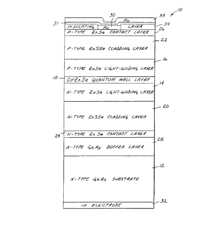
The structure of a laser diode 10 ln accordance wlth the
present invention is illustrated generally in Figure 1. Laser
dlode 10 is a wlde band gap II-VI device fabricated from
heteroepitaxial layers of ZnSxSel x~ ZnSe, and CdyZnl ySe grown by
molecular beam epitaxy (MBE) on a GaAs substrate. Prototypes of
this device have exhibited la~er action, emitting coherent blue-
green light near 490 nm from a CdyZnl ySe quantum well structure
under pulsed current in~ection at 77 K.
6 60557-4570D
CA 022345l7 l998-05-28
60557-4570
Laser diode 10 i8 fabricated on a GaAs sub~trate 12, and
lncludes lower (flr~t) and upper (~econd) ZnSe llght-guiding
layers 14 and 16,
60557-457OD
6a
CA 02234517 1998-05-28
~ _92/211~0 PCT/US92/0
respectiv~ly, ~teparated by a Cd~Zn~Se quantum well active
layer 18. The surfAces of light-guiding layers 14 and 16
opposite active layer 18 are bounded by lower and upper
ZnS~Se~ cladding layers 20 ~nd 22, respectively. A lower
5 ZnSQ ohmic contact layer 24 i~ positioned on the curface
of lower ~ ng layer 20 opposite light-guiding layer
14, while an upper ZnSe ohmic contact layer 26 is
positioned on the surface of upper cl~ ng layer 22
opposite light-guiding layer 16. A GaAs buffer layer 28
10 $eparate~ ~ubstrate 12 from lower ZnSe contact layer 24
to assure high crystalline quality of the contact and
su~sequently deposited layers. A polyimide insulating
layer 34 coYer~ the surface of upper ohmic contact layer
26 opposite upper cladding layer 22. Electr$cal contact
15 to the ohmic contact layer 26 iB made by Au electrode 30
which is formed in a window stripe in insulating layer
34. A t~in Ti layer 31 and subsequently a final Au layer
33 are applied over polyimide layer 34 and exposed
portions of Au electrode 30 to facilitate lead bonding.
20 Electrical contact to the lower sidQ of la~er diode 10 is
made by an In electrode 32 on the surface of substrate 12
opposite the lower ohmic contact layer 24.
Layers 24, 20 and 14 are all doped n-type with
Cl (ie., are of a first conductivity type) in prototypes
25 of laser diode 10. Layers 16, 22 and 26 are all doped p-
type with N (ie., are of a second conductivity type).
Active layer 18 is an undoped quantum well layer of
CdO2ZnO~Se semiconductor deposited to a thickness of 0.01
~m. Light-guiding layers 14 and 16 are both 0.5~m thick.
30 Lower light-guiding layer 14 i8 doped to a net donor
concentration of lxlO~7cm-3, while upper light-guiding layer
16 is doped to a net acceptor concentration of 2xlOI~cm-3.
Claddlng layers 20 and 22 are layer~ of ZnSOO7SeO93
sem~conductor depositQd to thickne-ses of 2.5~m ~nd
1.5~m, respectively. The net donor concentration of the
lower cladding layer is lxlO~3cm-3. The net acceptor
concentration of the upper cladding layer is 2xlO~7cm~.
60557-4570D
CA 02234517 1998-05-28
WC~ ~t~2117o PCI/US92/0378L
Ohmic contact l~yers 24 and 26 ar- both depocited to a
thickness of O l~m in these prototyp- d~vices The lower
contact layer i6 doped n-type to a net donor
concentration of lxlO"cm~ The upper contact layer i8
5 doped p-type to a net acceptor ~-o,~ tr~tion of lxlO~cm3
Other param-ter~ and materi~l~ can also be u~ed
in the fabrication of laser diode~ 10 in accordance with
the pre~ent invention For example, the thickne~se~ of
layers 24, 20, 14, 16, 22 and 26 can be vari~d as needed
lo for given applicat$ons Typical thicknQs6 rangQs for
contact, cladding and light-guiding layors ar- O 03 to
1 0 ~m, 0 5 to 5 0 ~m, and 0 1 to 1 0 ~m, re~pectivQly
In general, the thickne~-s of light-guiding layers 14
and 16 ~hould be chosen to minimize the width of the
15 optical mode If the layer~ 14 and 16 are too thin, the
evanescent tails will extend far into cladding layers 20
and 22 Cladding layers 20 and 22 must be thick enough
to make absorption of th- optical ~ode in ~ub~trate 12
and electrod~ 32 negligible The compo~ition of the
20 CdsZn~sSe (which det-rmines the la~er w~velength) with x
of approximately 0 2 was ~elected to provid~ rge
enough band gap difference (~ of approximately 0 2 eV)
to facilitate effective carrier confinement Larger x
will provide deeper quantum wQlls, but would require a
25 thinner layer due to increa~sd lattice mismatch, thereby
decreasing the efficiency of the collection of carrierC
into the well
The composltion of the ~nSy~ with y of
approximatQly 0 07 was ~ cted to provid~ ~ufficient
30 difference in refractive index from the index of the ZnSe
guiding layer~ to form a low-los~ wav-gulde Thl~
composition also provides excellent morphology since it
is nearly lattlce matched to the GaA~ ~ub~trat- at the
growth temperature of 300 C
Other n-type dopants which may b- u~ed include
Ga, Al, In, I, F, and Br Oxygen or Li acceptors can
also be used for the p-type dopants Other Group V p-
60557-4570D
CA 02234517 1998-05-28
~_g2/21170 PCT/US92/03
type dopants which might be u~d include ar~enic and
phosphorous. Greater donor and acceptor concentrations
can also be used, although they should not be 80 high as
to cause exce~ive free-carrier absorption.
The prototype~ of l~er diode 10 are fabricated
on Si-doped n~-type GaA~ ~ub~trat- 12 having a (100)
cry~tal orientation. Sub~trat~s 12 of this type are
commercially available from a number of manufacturers
including Sumitomo Electric Indùstries, Ltd. GaAs buffer
lO layer 28 is deposited to a thickness of 1 ~m in this
embodiment, and doped n+ with Si to a net donor
concentration of lxlOI~cm~3. Other appropriate 6ubstrates
(eg., ZnSe, GaInAs or Ge) and buffer layers such as
AlGaAs, AlAs, GaInP, AlInP, AlInAs or GaInAs can also be
15 used. The thickness of buffer layer 28 can al60 be
varied while providing an appropriate high-quality
surface for growing the II-VI semiconductors. If an
appropriate high-guality ~ub~trate and appropriate
surface preparation iB u~ed, buffer layer 28 may not be
20 needed.
The lattice con6tants of the ZnSSe cladding
layers 20 and 22 and the ad~acent ZnSe layers 24, 14 and
16, 26, respectively, are mismatched by about 0.3%.
Preliminary transmi6sion electron microscopy (TEM)
25 studies indicate that the ZnSe of light-guiding l~yers 14
and 16 is at least partially relaxed by dislocations
formed at the interf~ces of the light-guiding layers and
the adjacent ZnSSe cla~ng layers 20 and 22,
respectively. These preliminary ~tudies also indicate
30 that the thickness of the CdZnSe quantum well active
layer 18 is less than the critical thickne~R for this
material system. Quantum well active layer 18 is
therefore pseudomorphic, minimizing dislocations in the
light-emitting region of laser diode 10. The ~aximum
35 pseudomorphic thicknQs~es for ~trained epit~xial layers
~uch as 18 depends on the composition and can be
c~lculated from formulae describQd in MatthQws et al.,
60557-4570D
CA 02234517 1998-05-28
WC /21170 PCT/US92/0378~
-- 10 --
D~cts In Ep~t~x~al Mult~l~yer~, J. Cry~tal Growth, vol
27, p 118 ~1974) The inclusion of quantum well layer
18, which could al~o be ~ F~ Aomorphlc layer of other
semiconductor material such a~ ZnSeTe, facilitates the
5 low threshold curr-nt operatlon Or la~er diode 10 when
po~itloned within the thicker, low-lo~ II-VI waveguide
The waveguide can be made with higher r-fractlve index
light-guiding layers 14 and 16 ~nd lower refractive index
cladding layers 20 and 22 which can have a relatively
10 small dif~erence in their band gaps and need not be
exactly lattice m~tched The composition o~ the light-
guiding layers may be graded to minimize dislocations
and/or to form a graded index waveguide
Figure 2 is an illustration of a molecular beam
15 epitaxy (MBE) ~ystem 50 u~ed to f~bric~te the laser diode
10 described above MBE system 50 includes two MBE
chambers 52 and 54 interconn-ctet by ultrahlgh vacuum
(UHV) pipeline 56 Each chamber 52 and 54 includes a
high energy electron gun 58, a pho~phoruQ ~creen 60, a
20 substrate heater 90 and a flux monitor 6Z MBE chamber6
~uch a~ 52 and 54 are g~nerally known and commercially
available A Perkin-Elmer Model 430 MBE system was used
to produce the prototype la~er diodes 10
MBE chamber 52 i~ used to grow the GaAs buffer
25 layer 28 on sub~trate 12 and include~ a Ga erfu~ion cell
64 and an A~ cracking cell 66 A 8i efru~ion cell 6B iB
al60 provided ~B a ~ource o~ n-type dopant~ Substrate
12 i~ cleaned and prepar~d u~lng con~ntional or
otherwi~e known tec~n~ues, and mount-d to a Molybdenum
30 sample block (not shown in Fig 2) by In solder before
being positioned within chamber S2 By way of example,
substrate preparation t-c~n~ques de6cribed in th- Cheng
et al. articl~ Mol~cul~r-B-~m Eplt~xy Growth o~ 8nSe
Us~ng A Cr~c~c~d Sel en ~ um Source, J . Vac . Sc~ . Technol ,
35 B8, 181 (1990) were used to produc- the prototype laser
diode 10 The Si doped buffer l~yer 28 can be grown on
substrate 12 by operating MBE chamber 52 in a
60557-4570D
CA 02234517 1998-05-28
~2/21l70 PCT/US92/03
conventional manner, such ag that described in ~echnology
and Physics of Molecular Be~m ~p~t~xy, ed. E.H.c. Parker,
Plenum Pres~, 1985. The rQsulting ~uffer layer 28 ha~ an
As-rich ~urface which exhibited a c(4x4) reconstruction
5 as observed by reflection high energy electron
diffraction (Kh~ ). The sample block bearing the GaAs
substrate 12 and buffer layer 28 is then tran~fered to
MBE chamber 54 through UHV pipeline 56 for further
proces~ing.
Device layer_ 24, 20, 14, 18, 16, 22, and 26
are all grown on the buffer layer 28 ~nd GaAs substrate
12 within MBE chamber 54. To this end, chamber 54
includes a Zn effusion cell 70, cracked-Se effuqion cell
72, ZnS effusion cell 74 (as a source of S), Cd effusion
15 cell 76 and a standard Se (ie., primarily Se6) effusion
cell 79. A~ shown, cracked-Se effusion cell 72 includes
a bulk evaporator 84 and high temperature cracking zone
82, and provides a 60urce of cracked Se (including Se2 and
other Se molecules with les~ than 6 atoms). The bulk
20 evaporator 84 and high temperature cracking zone 82 used
to produce the prototype laser diodes lo are of a custom
design, the details and capabilities of which are
described in the Cheng et al. J. Vac. Sci. Technol.
article referenced above. Cl effusion cell 78 which
25 utilizes ZnCl2 source material provideR the Cl n-type
dopant. The p-type dopant i8 provided by N free-radical
source 80. Free-radical source 80 i8 connected to a
source 86 of ultra-pure N2through leak-valve 88. The
free-radical source 80 used in tbe fabrication of la6er
30 diodes 10 is commercially available from Oxford Applied
Research Ltd. of Oxfordshire, England (Model No. MPD21).
This ~ource ha~ a length of 390 mm. The beam exit plate
at the end of the 60urce is made of pyrolytic boron
nitride (PBN) and haq nine 0.2 mm diameter holes through
35 it. This source is mounted on a ~t~n~ard port for an
effusion cell through a lo" extension tube. N2 source 86
u~ed to fabricate la~er diode~ 10 i~ of re~earch purity
60557-4570D
CA 02234~17 1998-0~-28
grade produced by Matheson Gas Products. The pressure at the
inlet of the leak-valve of source 86 is 5 psi.
MBE chamber 54 is operated in the manner described
in the Cheng et al. article "Growth Of p- and n- Type ZnSe by
Molecular Beam Epitaxy", J. Crystal Growth 95, 512 (1989)
using the Se6 source 79 as the source of Se to grow the n-type
contact, cladding and light-guiding layers 24, 20 and 14,
respectively, of the prototype laser diode 10. Quantum well
active layer 18 is grown in a manner described in the Samarth
et al. article, "Molecular Beam Epitaxy of CdSe and the
Derivative Alloys Znl xCdxSe and Cd1 xMnxSe", J. Electronic
Materials, vol. 19. No. 6, p. 543 (1990).
MVE chamber 54 is operated in a manner described in
the Parker et al. article entitled "p-type ZnSe by Nitrogen
Atom Beam Doping During Molecular Beam Epitaxial Growth",
published in Appl. Phys. Lett. 57 (20), 12 November 1990,
using the Se6 source 79 to grow the p-type light-guiding layer
16 and cladding layer 22. Relevant portions of the above-
referenced article are summarized immediately below.
An atomic dopant beam (either nitrogen or oxygen),
produced by a free-radical source, is used to dope ZnSe during
molecular beam epitaxy which produces p-type ZnSe epitaxial
thin films. When electromagnetic power at the frequency of
13.52 MHz is coupled to an RF plasma discharge chamber of the
free-radical source, atomic dopant species are generated
inside the chamber of the free-radical source from a gaseous
source of ultra-high purity. A diffuser plate having 18 holes
of about 0.3 mm diameter each was used to separate the free-
radical source and the molecular beam epitaxy chamber. The
amount of the atomic dopant species generated is controlled by
the level of the RF power coupled to, and the pressure in the
RF plasma discharge chamber. The atomic dopant species, which
effuse into the molecular
60557-4570D
CA 02234517 1998-05-28
W~92/21170 PCT/US92/037
- 13 -
beam epitaxy ch~mber through openings in the diffuser
plate, are u~ed as the dopants during the molecular beam
epitaxy growth of ZnSe.
In one embodiment, ZnSe thin layers are grown
5 on a well-polished GaAs surface with the surfacQ normal
vector es~entially along the t0011 crystal orientation.
There are many ~uppliers of either the GaAs substrate,
available from, for example, Sumitomo Electric
Industries, Ltd., 1-1 Koyakita l-Chome, Itami, Hyogo, 664
10 Japan, or the GaAs epitaxial layer, available from Splre
Corporation, Patriots Park, ~edford, M~ chusett~,
01730, for this purpose. Before loading into the
molecular beam epitaxy sy6tem for the ZnSe growth, the
GaAs substrates are degrea~ed in trichloroethane,
15 acetone, and isopropanol, rinsed in deionized water and
blown dry by high purity nitrogen gas. The degreased
substrates are chemically etched in a solution consisting
of six parts of sulfuric acid, one part of hydrogen
peroxide and one part of deionized water for several
20 minutes (about two to five minutes). The substrate is
rinsed in deionized water and blown dry by high purity
nitrogen gas. The degreased and chemically-etched GaAs
substrates are t~en attached to a Mo samplQ block u~ing
molten In of high purity a~ solder. The ~ub~trate
25 assembly is immediately lo~ded into the molecular beam
epitaxy system. The GaAs substrates are heated in the
ultra-high vacuum growth chamber to about 610~C for a~out
one to five minutes to desorb the native oxides and
expose the underlying cry6talline strUcture on which the
30 ZnSe with the ~ame crystal 6tructure iB to be grown. The
typical growth conditions for ZnSe by molecular beam
epitaxy are a Zn to Se beam eguivalent pre~sure ratio of
1:2 (in the range of about 1:4 to 2:1) and a growth
temperature of 275~C (in the range of about 250~C to
35 400~C). Typical layer thickne~e~ and growth rate~ are
2 ~m and 0.5 ~m/h (in the range of about 0.4 ~m/h to
2.0 ~m/h) respectively. The atomic dopants generated by
60557-4570D
CA 02234517 1998-05-28
W~2/2ll70 PCT/US92/037~-
- 14 -
the free-radical ~ource ar~ incorporated into t~ ZnSe by
opening the mechanical 6hutter whicb block~ the line of
sight path betw~en t~e free-radical source and the heated
substrates
The ma~or focus in recent year~ r~g~rding
research on the wide-bandgap II~-VIA com~ou
~Qmiconductor, ZnS~ (~ ~2 67-Y at room tu~perature), has
b~en on producing low re~i~tivity p-type ~aterial Tbe
pr~sent invention utilize- a m~thod and apparatu~ for thQ
10 ln-situ production of ~pitaxial structur-~ comprising
ZnSe pn ~unction~ Thi~ i~ u~-ful in th- fabrication of
efficient light-emitting deYices, ~uch a~ light--mitting
diode~ and diode lasers which operate in the blue region
of the vi~ible ~pQctrum
Either nitrogen or oxygen are an excellent p-
type dopant element in ZnSe In addition to providing
large net acceptor densitie~ (greater than about 5xlO~Icm3
and low compQn~ation ~ND/NA le~ than about 0 8)),
nitrogen and oxyg-n ar~ ~tabl~ ln ZnSe at t-mp-ratures up
20 to 375~C
Large concentrations of net nitrogen acceptor
impuritie~ are incorporated into ZnS~/GaA~ ~pitaxiA1
layer6 which involves nitrogQn atom beam doping during
molecular beam epitaxial growth Net accQptor d~n~ities
25 as largQ as 4 9xlO~7cm3 hav~ b-en m~asured in th~ re~ultant
p-type ZnSe material
Fig 9 ~hows a mol ~ r b~am ~pltaxy cy~t~m
110 MolQcular beam ~pitaxy ~y~tem 110 includes a
molecular b~am epitaxy chamber 112 which ~nclo~-s a
30 6ubstrate 114 NolQcular b~am epitaxy chamb-r 112
~ncludes an electron gun 116, a rho~horus scr-en 118 and
a flux monitor 120 Effusion cell~ 122, 124, 126, and
128 are carried in molecular beam epitaxy chamber 112
Effueion cells 122, 124, 126, and 128 may compri~e, for
35 example, effusion cells for Zn, Se, and ZnCl2 Molecular
beam epitaxy ~y~tem 10 also includes a free-radical
source 130 Free-radical source 130 may comprise a
60557-4570D
CA 02234517 1998-05-28
W~J ~2/21170 PCI'/US92/03;....
source of any group VA or oxygen free-radicals. For
example, free-radical source 130 may provide a ~ource of
nitrogen free-radicals, in which free-radical source 130
is supplisd with ultra-pure Nl fro~ ~n ultra-pure N2
5 ~ource 132 through a valve 133. Fr-e-radical ~ource 130
is available from Oxford Applied Rer-Arch Ltd.
(Oxfordshire, UK). Free-radical source 130 might
comprise other type~ of sources which produce free-
radicals. For example, an electron cyclotron resonance
(ECR) free-radical 60urce may be u~ed (available from,
for example, Wavemat, Inc., 44780 Helm Street, Plymouth,
Michigan). A microwave cracker coupled into the gas
source through a microwave tube may be used to produce
free-radical~. A DC plasma di~charge chamber may also be
15 used. Furthermore, any appropriate thermal cracker or
disassociation cell (available from, for example, EPI,
261 East Fifth Street, St. Paul, Minnesota 55101) may be
used.
ZnSe layers were grown on GaAs sub~trates in a
20 molecular beam epitaxy sy6tem of the type described
herein. The6e layers were grown at a substrate
temperature of 275~C with a Zn to Se beam equivalent
pressure ratio of 1:2 (typical layer thickne66es and
growth rates were 2 ~m and 0.5 ~mth, rQspectively).
25 P-type doping of the ZnSe layers wa8 achieved by a free-
radical source which was incorporated in the molecular
beam epitaxy system, rather than a conventional effusion
source. The free-radical 60urce provided a flux of
atomic nitrogen (together with a much larger flux of non-
30 di6sociated N2) created in a RF plasma di6charge chamber
A RF frequency of 13.5 MHz was used to generate nitrogen
atoms from a ga6eous source of ultra-pure N2. The atomic
nitrogen flux level was controlled by suitably adjusting
the intensity of the RF plagma discharge.
The nitrogen actively incorporated into the
ZnSe was much greater using the free-radical atomic beam
than that of molecular nitrogen, a~ evidenced by
60557-4570D
CA 02234~17 1998-0~-28
comparing lOK photoluminescence (PL) spectra recorded from
ZnSe layers grown with a flux of N2 only and with a flux of N
+ N2. As shown in Figs. lOA1 and A2, the lOK PL spectrum
recorded from a ZnSe layer grown using a flux of N2 only, (in
this case an equilibrium background pressure of N2 in the
molecular beam epitaxy chamber of 5x10⁻⁷ Torr was maintained)
appears to be identical to that recorded from undoped ZnSe
heteroepitaxial layers (see R.M Park, C.M. Rouleau, M.B.
Troffer, T. Koyama, and T. Yodo, J. Mater. Res., 5, 475
(1990)). The dominant peaks in the excitonic regime are the
split free-exciton (Ex) and donor-bound-exciton (I2)
transitions, the splitting being due to the thermal expansion
coefficient mismatch between ZnSe and GaAs which renders the
ZnSe layers under inplane biaxial tension (see K. Shahzad,
D.J. Olego, D.A. Cammack, Phys. Rev. B 39, 13016 (1989)).
Consequently, at such low background N2 partial pressures,
molecular nitrogen is completely unreactive at the ZnSe
surface. The situation changes dramatically, however when a
plasma discharge is created in the free-radical source, as
shown in the lOK spectrum of Figs. lOB1 and B2. Again the
background N2 partial pressure in the molecular beam epitaxy
chamber during growth was 5x10⁻⁷ Torr with power applied to
the RF plasma discharge. The excitonic regime is dominated by
split acceptor-bound-exciton (IN1) transitions due to the
incorporation of nitrogen acceptor impurities (see P.J. Dean,
W. Stutius, G.F. Neumark, B.J. Fitzpatrick, and R.N. Bhargava,
Phys. Rev. B 27, 2419 (1983)). In addition, the complete PL
spectrum is dominated by donor-to-acceptor (D-A) transitions
(QNO-represents the no phonon transition, with several LO
phonon replicas of QNO also indicated) as opposed to excitonic
transitions. Thus, the rate of substitutional incorporation
of atomic nitrogen is much greater than that of molecular
nitrogen at the growing ZnSe surface. The sample from which
the PL spectrum shown in Figs. lOB1 and B2 was obtained was
found to have a net acceptor concentration of lxlO17cm~3.
- 16 -
60557-4570D
CA 02234517 1998-05-28
W~92/21170 PCT/US92/03
- 17 -
Net acceptor concentrations, NA-ND, in the
nitrogen doped ZnSe/GaAs layers were determined using
capacitance-voltage (C-V) profiling. Since the ZnSe
epitaxial layers were ~ .. on semi-insul~ting GaAs,
5 planar profiling between two Schottky contacts on the
ZnSe surface was carried out. T~e surface contact
pattern consisted of a ~eries of 762 ~m diameter Cr/Au
dots physically isolated from a large Cr/Au ~lL~unding
electrode. The separation between the inner (dot)
lo electrodes and the outer electrode was 25 ~m, a sm~ll
separation being necessary ln order to maintain a low
series resistance. The contact pattern was created by
thermally evaporating 75 ~ of Cr followed by lOOo A of Au
and performing photolithographic and lift-off processes.
15 In all of these measurements the outer electrode was held
at ground potential and bias was applied to the inner
Schottky contact.
With this sign convention the ma~ority carrier
type is given by the sign of the slope of the l/C2 versus
20 V plot; a pOfiitiVe slope would indicat~ th~ material to
be p-type. The net acceptor (NA-ND) concentration is
proportional to the slope of l/C2 versus V. The l/C2
versus V plot and the NA-ND ver~us depletion width profile
obtained from a heavily-doped ZnSe layer are illustrated
25 in Figs. ll(a) and ll(b), respectively. As 6hown in
Figs. ll(a) and ll(b), the material is p-type with a net
acceptor concentration around 3.4xlOI7cm-3. As shown in
Fig. ll(b), the doping profile is rather flat from zero
bias (0.068 ~m) out to where rever~e bias breakdown
30 occurs (1.126 ~m). Breakdown o~ L~d at 3.8 V which is
consistent with avalanche breakdown in ZnSe material
doped at this level, ie, 3.4xlO~cm~3 p-type.
Further evidence of the p-type nature of the
nitrogen doped ZnSe material was obtained through the
35 fabrication of blue light-emitting diodes based on
epitaxially grown ZnSe:N/ZnSe:Cl pn homo~unctions. The
n-type ZnSe layers in the~ pn ~unctions were grown using
60557-4570D
CA 02234517 1998-05-28
w092/2l170 PCT/US92/03782
- 18 -
Cl as th~ dop~nt QlemQnt, t~Q ~ource Or the Cl atom~
being a ZnClt effusion cell inco~v~ated in the molecular
beam epitaxy ~ystem
~ number of ZnSe ~amples grown u~ng molecular
S beam epltaxy were tested The r~ult6 were a~ follow~
1 Undoped Zn8e
Zn to Se b-a~ eguivalent pressure
ratio 1 2
lo Growth Temperature 275 C
Results Low t-mp-rature
photolumine~cence ~pe_L~um indlc~ted
sample wa~ not p-typs C-Y
mea~urem-nt indicat-d ~mple was
in~ulating
2 Doped ZnSe u~ing N~ with no RF power to
free-radical source
Zn to Se beam eguivalent pressure
ratio 1 2
Growth Temperature 275 C
RF power 0 watt~
Backyr~ul~d pre~ure 5x10⁻⁷ Torr
Result~ Low temperature
photoluminescence spectrum indic~ted
~ample wa~ not p-type C-Y
mea~urements indicated ~mple was
in~ul~ting.
3 Doped ZnSe using N2 wlth RF pow~r to free-
radical ~ource
Zn to S- b-am equivalent pre~ure
ratio 1 2
Growth temperature 275 C
RF power 320 watt~
Background pre~sure 5x10⁷ Torr
Re~ult~ Low tempQrature
60557-4570D
CA 02234517 1998-05-28
~._92/21170 PCT/US92/03 _
~ -- 19 --
photoluminocr~nc~ spectrum, current-
voltage mea~urement ~nd capacitance-
voltage mea~urement lndicated that
sample was p-type. ND/N~SO.8 (high
doping efficiency) and NA-
ND=3 . 4xlO~7cm~3.
4. Doped ZnSe using ~2 with RF power to free-
radical source:
Zn to Se beam equivalQnt pressure
ratio: 1:2
Growth temperature: 275~C
RF power: 3 20 watts
~ackground pre~sure: 5x10⁻⁷ Torr
Results: Low tempersture
photoluminescence ~pectrum, current-
voltagemeasurement, and cap~citance-
voltage measurement indicated that
sample wa6 p-type and N~-
2 0 ND-3 . OX10~6Cm-3 . .
Fig. 12(a) ~hows a light emitting diode 134.
Light emltting diode 134 includes a p-type GaAs ~ub~trate
136. P-type GaA~ substrate 136 forms the base for
25 molecular beam epitaxial growth. A p-type ZnSe nitrogen
doped layer 13 8 is depo6ited upon p-type GaAs substrate
136. P-type ZnSe layer 138 i~ deposited in accordance
with the present invention u~lng a nitrogen free-radical
source. An n-type ZnSe chlorine doped layer 140 is
30 deposited upon p-type ZnSe layer 138. An n+ ZnSe cap
layer 142 is deposited upon n-type ZnSe layer 140. The
deposition of layers 138, 140, and 142 i5 through
molecular beam epitaxial growth. Ohmic contact~ 144 and
146 form electrical contacts to n~ ZnSe cap layer 14Z and
35 p-type GaAs substrate 136, respectivQly. I n o n e
embodiment, p-type ZnSe layer 138 has a thickness of 2~m
and has a net acceptor concentration o~ 1xlol~cm-3. N-type
60557-4570D
W('~2/21170 CA 02234517 1998-05-28 PCT/US92/03
- 20 -
ZnSe l~yer 140 has a thickness of O 5 ~m ~nd a net donor
concentr~tion of lxlO1~cm3 The n~ ZnSe cap layer 142 has
a thickness of 500 A and a net donor concentration of
SxlO~cm3
s Fig 12(a) shows th- p-typ- ZnSe layer iB grown
fir~t on a p'-typ~ GaA~ ~ubstrate Thi~ type of "buried
p-type layer" structure avoids the ~erious problems
associated wlth ohmic contact formation to p-type ZnSe
(See M A Ha~se, H Ch~ng, J M DePuydt, and J E Potts,
lO J Appl Phys , 67, 448 (l990)) However, a di~advantage
with this device design iB that a large hole b~rrier
exlsts At the p~-GaAs/p-ZnSe h-tero-interface (~ee L
Kassel, H Ab~d, J W G~rland, P M Raccah, J E Potts,
M A Haase, and H Cheng, Appl Phy6 Lett , 56 42
(1990)) In tbis type of de~ice, hole in~ection across
the p+-GaA~/p-ZnSe hetero-interface i~ only realized ~t
~val~nche breakdown Con~-quently, large turn-on
voltages are required to observe electroluminescence
associated with the ZnSe pn homo~unction
Light-emitting diod~ rabrication wa6
accomplished u~ing conventional photolithographic
techniques with devicQ i~olation being achieved by wet
chemical etching to form 400 ~m diameter me~as The top
electrode metalization was ring shap-d and w~ p~tterned
25 by vacuum evaporation and lift-orf Ultrasonic gold ball
bonding was used to make cont~ct to the devices for
electroluminescence characterization
A typical electrolumine-c-nc- ~pectrum r-corded
at 77K for light emitting diode 134 ~hown in Fig 12(a),
30 is illustrated in Fig 12(b) Th- device operating
voltage ~nd current were 13 5 V ~nd 40 mA, r~spectlvely,
for the ~pectrum ~hown in Fig 12(a) A~ c~n be ~een
from Fig 12(b), the visible electrolumine~cence is
dominated by blue emis~ion, the spQctrum comprising
35 number of resolved line~ principally at 447 7 nm, 459 6
nm and 464 7 nm The two highest energy peaks in the
spectrum corre~pond clo~ely in energy to the
60s57-4s70D
CA 02234517 1998-05-28
W~92~21170 PCT/VS92/037
electroluminescence peaks ob~erved at 77~ from blue
light-emitting diodes fabricated using a nitrogen-ion
implantation and annealing procQdure as reported by
Akimoto et al (See K. Akimoto, T. Hiyajima, and Y. Mori,
5 Jpn. J. Appl. Phys., 28, L528 (1989)). Infrared emission
at 844 nm was al~o recorded from the~e devices
(simultaneously with the blue emis~ion) which appear~ to
be the result of electron injection into the p+-type GaA~
material under avalanche breakdown conditions at the
lo hetero-junction (not shown in Fig. 12(b)).
An electroluminescence spectrum recorded at
room temperature from the devlce 6tructure illustrated in
Fig. 12(a) (visible region only) is ~hown in Fig. 13. As
can be seen from the figure, dominant emission in the
15 blue region of the visible spectrum is observed, peaking
in intensity at a wavelength of 465 nm. For the
particuIar spectrum ~hown in Fig. 13, the voltage applied
and current drawn were 22 V and 20 mA, respectively.
Fig. 14 shows a light emitting diode 148.
20 Light emitting diode 148 is a p on n device which
operates similar to light emitting diode 134 of ~ig.
12(a). Light emitting diode 148 includes an n~ GaAs
substrate 150, an n-type ZnSe layer 152 and p-type ZnSe
layer 154. Contacts 156 and 158 make electrical contact
25 with p-type ZnSe layer 154 and n+ GaAs ~ubstrate 150.
The p-type ZnSe layer 154 i~ deposited using molecular
beam epitaxy and a group VA free-radical source described
above. In one embodiment, diode 148 shown in Fig. 14 n-
type ZnSe layer 152 has a net donor concentration of
30 about lxlO~cm-~ and a thicknes~ of about 2.0 ~m and p-type
ZnSe layer 154 has a net acceptor concentration of about
lxlO~7cm~3 and a thickness of 0.5 ~m.
Using the method and apparatus de~cribed above,
n-type IIB-VIA semiconductor film may alco be produced.
35 The resultant IIB-VIA semiconductor film may be used in
pn junction devices such as light emitting diodes and
light detectors as well as diode lasers and transistors.
60557-4570D
CA 02234517 1998-05-28
W ~ ~/21170 PC~rJUS9210378
The free-radical source i~ in-~Gd~ced into a molso~llar
bQam epitaxy growth chamber to provldo a dopant to a IIB-
VIA ~e~iconductor during mol~cul~r bQam opltaxial growth.
The free-radical source ~ay be nitrogen, phosphorus,
5 arsenic, and anti~ony. Oxyg-n ~ay al~o be used as a
~uitable free-radical ~ource. The method and appar~tus
may be used for N-doping and O-doping of ZnSe. P-type
tern~ry II~-YIA semiconductor~ including Zn~Cd~Se, ZnSe~
~Te~, ZnSe~S" ZnSI~Te~, and Zn~Cd~S.
lo Referring again to Figure 1 and th- pr-sQnt
invention, lower ZnSSe cla~in~ layer 20 iB doped n-type
using the ZnCl2 ~ource. Other a~pect~ of the tsr~n~ques
used to grow cladding layers 20 and 22 are de~cribed in
the M~t~umur~ et al. article, Opt~mum Compos~t~on In MB~-
15 ZnS~Se~JZnS~ For ~gh QU~l~ty ~teroep~t~l Growth, J.
Crys. Growth, vol. 99, p. 446 (1990).
A low resistivity p-type Zn8e ohmic contact
l~yer 26 has been achieved by growing the contact layer
at low temperature within MBE chamber 54 utilizing the
20 cracked Se source 72 (ie., cracking zone 82 and
evaporator 84), while at tho came time doping the
se~lconductor material of the contact l~yer p-type in
accordance with the method d~cribed above. The low
temperature growth technique usQd to produce the contact
25 layer 26 of the prototype laser diode 10 i~ deficribed
generally in th~ ChQng et al. article Low Temper~ure
Growth O~ ZnS~ By Nolecul~r Be~m Ep~t~xy Us~ng Cr~cked
Selen~um, Appl. Phy~. Lett. (Feb. 1990). The
~emiconductor body with layer~ 28, 24, 20, 14, 18, 16 and
30 22 on ~ubfitrato 12 i~ heated to a temperatur- le~ than
250~ C but high enough to promote cry~talllne growth of
the ZnSe doped with the N p-type dopant~ to a net
acceptor concentration of at lea~t lx1017cm~. A net
acceptor roncQntration of lxlOI~c~3 wa~ achieved in the
35 ohmic contact layer 26 of prototype la~er diod-c 10, wh~n
grown at a substrate temperatur- of about 150- C.
How~ver, it is anticipated that ohmic contact layer~ 26
60557-4570D
CA 02234517 1998-05-28
J2ttll70 PCT~US92/03
- 23 -
with acceptable characteristics can be achieved at other
growth temperatures down to at least 130~ C. Other
operating parameters of MBE chamber 54 used to produce
the ohmic contact layer 26 of the prototype la~er diodes
5 10 are as follows:
Zn beam equivalent pressure: 1.0x10⁷ Torr*
Se cracking zone temperature: 600~ C*
Se bulk ev~porator temperature: 250~ C*
Growth rate: 0.3-0.6 ~m/hr
Surface rQconstruction: Zn-stabilized
Nitrogen pressure in chamber: >3.5x10⁷ Torr*
rf power: 150-250 ~
* parameters dependant upon specific MBE system
configuration
Figure 3 is the current-voltage characteristic
of a sample with two coplanar Au metal electrodes on a p-
type ZnSe contact layer produced for test purposes in a
20 manner substantially similar to that described above.
The ohmic nature of this contact is indicated by the
substantially linear nature of the curve over the -6 to
+6 volt range.
The mechani~ms believed to enable the ohmic
25 nature of contact layer 26 can be described with
reference to Figure 4 which is an energy band diagram of
the Au - p-type ZnSe contact layer interface. In
addition to the expected shallow impurities 100 utilized
by conventional ohmic contacts, additional electronic
30 energy states 102 are formed in the contact layer. These
additional energy states 102 are relatively deep (within
the forbidden gap) with respect to the valence band
maximum, campared to the depth of the shallow impurity
level 100. Energy states 102 are in effect intermediate
35 energy states located at an energy less than the Au Fermi
level and greater than the ~hallow impurity level 100.
Since the probability of charge carriers tunneling
60557-4570D
CA 02234517 1998-05-28
W~ /2ll70 PCT/US92~0378
- 24 -
between two given energy states incr~ YponQntially
with decreasing distance between the two ~tates,
additional energy ~tates 102 greatly increase the
tunneling probability by prov~d~ng a t-mporary re~idence
5 for the carrier~ and facilitate ~ulti-~tep or cascade
tunneling. The optimum condition is illu-trated in
Figure 4 where Ep is the ~ermi energy and E~ i~ the
acceptor energy. A diagramatic depiction of an electron
making a multi-step tunneling transfer between the ZnSe
lo and Au layers through the additional energy state~ 102 i6
also ~hown in Figure 4. Even better cont_cts are
attainable with electronic state~ ~t more than one energy
level, ~uch that tunneling can occur from ~tate to ~tate
across the barrier.
It i~ anticipated that the introduction of
additionsl energy 6tates 102 can be achieved by a number
of methods. Doping during growth, diffusion, ion
implantation or other known t~c~niques can be used to
incorporate impurities whlch produce deep l-vel~. One
20 import_nt type of deep level impurity is the i50-
electronic trap. ~y way of example, Te iB thought to
form a hole trap in ZnSe. The _dditlonal energy ~tates
102 can also be achieved by introducing proper native
crystal defects ~uch a~, but not limited to,
25 di~locations, vacancies, interstitials or co~plexes into
contact layer 26. Thi~ can be dona during the daposition
of the contact layer by choo~ng tha molecular 8pecie~ of
the precursor~, and/or by other appropriate growth
condition6. Native defect~ can also be generated by
30 post ~wth treatment~ such a~ ~rradiation by electron
beams, ion b-ams, radical b-ams or el-ctromagnetic
radiation. However, thasa te~hn~ques mu~t be implemented
without detrimentally degrading the conductivity of the
ZnSe or other ~emiconductor material u~ed for the contact
35 layer.
It therQfore appQ_rs that the u~eful p-type
contact ~ayer 26 ha~ a number of propertie~. The net
60557-4570D
CA 02234517 1998-05-28
W~ ~2/21170 PCTJUS92/03
acceptor density NA-ND is large, preferrably at least
lxlO~cm3. This serves to reduce the width of the barrier
through which the charge carriers must tunnel. The p-
type dopant concentration (nitrogen in laser diode lO)
5 must also be larqe, preferrably at least lxlO~9cm-3. In
addition to forming the ~hallow acceptor levels, the
nitrogen impurities also appear to participate in the
formation of the deep energy states. At a minimum, the
amount of nitrogen required is that which will provide
10 adequate concentrations of both types of levels. The
growth conditions must also be appropriate to form the
defects at the energy levels de~cribed above. The low
temperature growth technique described above has been
shown to produce these material properties (contact
15 resistances less than 0.4 ohm-cm2 have been achieved).
The low-temperature photoluminescence (PL)
spectrum from a good ohmic contact layer such as 26 is
shown in Figure 8. The observed characteristics include:
l) the very weak near band edgQ PL; 2) the appearance of
20 the defect band at 2.3 eV (18,500 cm-l); and 3) the
presence of a band (presumably a~sociated with donor-
acceptor-pair recombination) at about 2.5 eV (20,400 cm~
The band edge PL is expected to be weak for materials
which have significant concentrations of deep levels
25 since the deep levels provide long wavelength and
nonradiative channels which compete with the near band
edge proce~ses. The emission band at approximately 2.3
eY is as~ociated with a transition from the conduction
band to a deep (acceptor) level about 0.5 eV above the
30 valence ~and maximum. Thi~ is near the energy position
that iB believed to be the most effective for cascade
tunneling. The emission band at 2.5 eY i8 believed to be
related to transitions from donor to acceptor states. No
or minimal donor states would be preferrable, eliminating
35 this transition, or shifting its occurance to ~lightly
higher energies.
60557-4570D
~'() ~2/21 1 7U CA 0 2 2 3 4 517 19 9 8 - 0 5 - 2 8 PCl tUS9t~0378
-- 26 --
I
In g~ner~ nd other than the d$frer-nce~
de~cr$bQd below, conventional procs-~e- (ie , tho~e us~d
for Si and III-V semlconductor devices) arQ used to
complete the fabrication of prototype laser diode 10
5 Following the deposition of contact layer 26, the as yet
incomplete la~er diode 10 i~ removed from MBE chamber 54
Electrode 30 includes Au which is ~acuum avaporated onto
contact layer 26 and patterned into a 6tripe (typically
~bout 20 ~m wide) u~ing conventional photollthography and
lo llft-off An in~ulating layer 34 of i~ then ~pplied ov-r
electrode 30 and th~ expo~ed ~urface of contact layer 26
~or an insulator that can be applied at low temperatures,
polyimide photoresi~t i~ preferred Prob$m$de 408 from
Ciba-Geigy Corp wa~ used to produce laser diode 10 A
15 stripe (about 20 ~m wide) of the polyimide layer 34
directly above electrode 30 i~ removed by UV exposure
through ~ photomask ~nd d~v-lopment u~ing the
manufacturer's recommended pl~ ~sing recipe, ~xc ~L for
the post-developmQnt cure To cure the dQveloped
20 polyimide, the devic~ wa~ flood exposed to 1 J/C~2 of W
light from a mask aligner, and baked at 125~ C on a hot
plate in ~ir for 3 minute~ Ti-Au layer 31 iB th-n
evaporated on the expo6ed ~urface of the Au electrode 30
and polyimide layer 34 to facilitate lead-bonding The
25 In used for MBE substrate bonding ~180 ~er~ed a8
electrode 32 on substrate 12 Opposite end~ of the
device were cleaved along (110) plane~ to form facQt
mirrors Cavity length of the prototype devices 10 i~
about 1000 ~m La-er dioae~ 10 werQ then bond-d p-side
3Q up to cer~mic sampl- hold-r~ wlth ~ilvQr-fllled ~poxy
Improved performanc~ of th-~e l~er deviceR can
be gained by providing bett~r lateral confinement of the
optical mode This can be achieved by forming an index-
guided la~er 10' such as that ~hown in Figure 7 Index-
35 guided laser 10' i5 6imilar to la~er lO ~nd can befabricated with the 6ame II-VI ~emiconductor layers
Portions of l~er 10' which corre~pond to tho~e of l~ser
60557-4570D
CA 02234517 1998-05-28
2/21170 PCT/US92/03
- 27 -
lO are indicated with identical but primed (ie., "X"')
reference numer~ls. In the embodiment shown, laser lO'
includes a waveguide or rib 35 in the cladding layer 22'
and contact layer 26'. Rlb 35 can be formed to a width
5 of about 5 ~m by ion beam etching with a Xe or Ar ion
beam or by wet-chemical etching. Conventional
photoresist can be uRed as a ma~k for this process.
other known and conventional techniques can al~o be used
to provide lateral waveguiding. These techniques include
lO using ~ubstrates in which grooves h~ve been etched (ie.,
channelled-subRtrate la~er~), or etching a rib and re-
growing a top cladding layer (ie., a "buried
heterostructure" laser). Im~rovements in the threshold
current or the differential quantum efficiency may be
15 achieved by dielectric coatings of the facets to adjust
the reflectivities.
Initial tests of the prototype laser
diodes lO were conducted at 77 X by pulsing the devices,
typically with 500 n~ec pul~es and a 500 ~sec period.
20 Current measurements were made with a box-car averager,
while a large Si photodetector wa6 u~ed to collect and
monitor the output light intensity from one end facet of
the device. The measured light output as a function of
current (ie., L-I) characteristics from one of the
25 devices is illustrated in Figure 5. The threshold
current is 74 mA, whlch corrQ-ponds to a threshold
current density of 320 A/cm2. Differential quantum
efficiencies in excQss of 20% per facet have been
measured, as have pulsed output powers of over lO0 mW per
30 facet. The coherent light is ~trongly TE polarized and
a "speckle pattern" is clearly vi~ible. The output laser
beam has an elliptical far-field pattern, with a
divergence of roughly 40~x4~ for the central lobe. Side
lobes are visible, indicating higher order transverse
35 modes.
The mea~ured L-I characterictics, ~uch as that
shown in Figure 5, do indicate some dependence on pulse
60557-4570D
CA 02234~17 1998-0~-28
length. At high current densities, the gain in the single
quantum well prototype devices tends to saturate. At the same
time, the index of refraction is reduced due to the injection
of excess carriers, which tends to make the region under the
stripe of electrode 30 anti-guiding. Thermal effects become
important at these current densities as thermal gradients and
the temperature dependence of the index provide lateral
optical confinement. It is expected that these
characteristics will be alleviated by index-guided versions
such as laser diode 10'.
Figures 61 and 62 show a graph of the optical
spectra that are characteristic of the prototype laser diodes
10 at 77 K. The spectra illustrated in Figures 61 and 62 were
acquired using a SPEX 1403 double monochromator. At currents
below threshold, the spontaneous emission occurs at 490 mn and
has a FWHM of about 3nm. Above threshold, the 1060 ~m long
device operates in many longitudinal modes centered at 489.6
~m, and which are separated by 0.03 nm.
Laser operation has been observed in the prototype
laser diodes 10 for short periods of time at temperatures as
high as 200 K. At room temperature the devices emit at 502
nm, but do not lase.
The operating voltage of the prototype laser diodes
10 at the threshold current is approximately 15 V. This
characteristic indicates that there is still room for
improvement in the ohmic contact between electrode 30 and
contact layer 26 and/or improvement in the conductivity of p-
type layers 16, 22, and 26. Reducing this series resistance
and improving the heat-sinking of the device (ie., by solder-
bonding the p-type side down) are expected to facilitate CW
operation at higher temperature.
It is expected that the inventive concepts disclosed
herein and used to fabricate the prototype laser diode 10 are
equally well suited to the fabrication
- 28 -
60557-4570D
CA 02234517 1998-05-28
~ ~2t21170 PCT/US92/03
-- 2g --
of laser diodes from a wide variety of other compound II-
VI 5emiconductor alloy6, eBpecially from other ZnSe
alloys. For example, improved operatlng character~sics
will be achieved by using lattice matched materials such
5 ag Cd~Zn~S (with x of a~uximately 0.61) and ZnSe to form
the waveguide. The quantum well in 6uch a device may
include CdZnSe. ThiA ~emiconductor 6ystem will not
suffer from misfit dislocation~ which c~n decrease
efficiency and the useful li~etime of the devices. Also,
lo a multiple quantum WQll active layer made of a ~trained-
layer superlattice could replace the 6ingle pseudomorphic
quantum well layer 18.
Ohmic contact layer 26 might also be improved
by using thin layer~ of smaller band gap II-VI alloys
15 such as ZnSel~Tes, C~Znl~Se and Hg~Znl,Se. Group YI sources
other than Se2 can al~o be used to produce ohmic contacts
in accordance with the present invention. Other Group VI
specieR Xm wher- m<6, ~ w-ll a- other ~ource~ of the~Q
speciQs, should be suitable substitutQ~. Other metals
(eg., Pt) or other electric~lly conductive materials
having a large work function (eg., >5eV) and ~uitable for
a stable semiconductor interface can also be used as
electrodes. In conclu~ion, although the present
invention has been described with reference to preferred
25 embodiments, change~ can b- mads in form and detail
without departing from the ~pirit and scope of the
invention.
60557-4570D