Note: Descriptions are shown in the official language in which they were submitted.
CA 02234~32 1998-04-09
SVG-4016
MULTIPLE DETECTOR ALIGNMENT SYSTEM
FOR PHOTOLITHOGRAPHY
FIELD OF THE lNVL~ lON
The present invention relates generally to photolithography
as used in the manufacture of semiconductors, and more
specifically to a multiple purpose detector used to provide
imaging information.
R7~C'Kti:ROUND OF THE lNV~ lON
The manufacture of semiconductor circuits has as a key step
the use of photolithographic techniques. In the
photolithographic process, there is a need to position a wafer
coated with a photosensitive compound, generally known as photo
resist, relative to the image of a mask or reticle containing
circuit patterns thereon. Because the processing requires
multiple layers to be placed on the wafer, precise positioning of
these multiple layers is required. The position of the reticle
image and the wafer often must be known and aligned within a
range of some nanometers.
One such alignment system is disclosed in U.S. Patent
4,697,087 entitled "Reverse Dark Field Alignment System For
Scanning Lithographic Aligner" issuing to Frederick Y. Yu on
CA 02234~32 l998-04-09
SVG-4016
September 29, 1987, which is herein incorporated by reference.
Therein disclosed is an alignment system wherein a wafer having a
wafer target thereon, and a mask having a mask target thereon,
are aligned with respect to each other. In this alignment
system, a target on the wafer and a target on a reticle are
scanned relative to each other. The reflected light is detected
and compared to determine any misalignment. Another alignment
system is disclosed in U.S. Patent 4,549,084 entitled "Alignment
And Focusing Systems For Scanning Mask Aligner", issuing to David
A. Markle on October 22, 1985, which is herein incorporated by
reference. Therein disclosed is an alignment system employing a
pattern on the mask and wafer including optical grids
corresponding to the directions and spacing of the patterns so
that light transmitted through the grids is strongly modulated.
The light modulated from the mask and wafer alignment targets is
used to obtain alignment error signals, as well as to measure how
well the mask is focused on the wafer. Another alignment system
is disclosed in U. S. Patent 5,477,057 entitled "Off Axis
Alignment System For Scanning Photolithography", issuing to
David Angeley et al on December 19, 1995. Therein disclosed is
an alignment system having multiple detectors for detection of
light scattered and reflected from alignment marks placed on a
wafer.
CA 02234~32 1998-04-09
SVG-4016
While these alignment systems have proven adequate for their
intended purpose with scanning photolithography and continuous
light sources, they may have difficulty providing adequate
alignment signals in other applications, for example, with use of
pulsed illumination sources, or static or stepped
photolithography techniques where scanning may not be employed.
Therefore, there is a need to provide adequate alignment between
a reticle and a wafer when a pulsed illumination source is used,
as well as not being dependent on the scanning movement of a
reticle and wafer in order to obtain alignment information.
Additionally, there is a need to obtain other image information
from a single detector that is relatively simple and easy to
manufacture or modify, depending upon the particular application
and imaging information desired, such as focus or image quality
monitoring.
St~lARY OF THE INVEN~ION
The present invention is directed to a detector and system
used in obtaining imaging information, such as aligning a reticle
to a pre-existent pattern on a semiconductor wafer via alignment
of the reticle image to the pattern pre-existent over a detector
array and/or obtaining image quality information. The image of a
reticle having predetermined apertures therein is projected onto
CA 02234~32 1998-04-09
SVG-4016
a detector placed on an X-Y stage. The detector has a
photosensitive layer forming a rectangular or other regular array
of individual elements or cells, such as a CCD or charge coupled
device. Covering a portion of the photosensitive layer is an
opaque layer. The opaque layer has predetermined openings
matched to the apertures in the reticle. The openings are
configured such that positioning and image quality information,
such as focus and astigmatism, are obtained from the signal read
from the individual elements. The image of the reticle,
illuminated by a source, is projected by a projection optic onto
the predetermined or matched openings in the opaque layer,
thereby generating a signal. Multiple openings can be used on a
single monolithic photosensitive element, with the detector being
divided into sub-detector regions. One sub-detector region,
which may have multiple independent individual elements, has
openings in the opaque layer for determining position by
balancing the illumination from filled or exposed portions of
adjacent openings. The illumination filled portions are
illuminated by a predetermined illumination pattern from
apertures in the reticle. Other sub-detector regions detect
image quality, such as focus and astigmatism by projecting the
image of predetermined or matched apertures in the reticle onto
predetermined or matched holes in the opaque layer. In one
CA 02234~32 1998-04-09
SVG-4016
embodiment, optimum focus is obtained by focusing a predetermined
illumination pattern onto a predetermined opening, and maximizing
the signal. In another embodiment, astigmatism is obtained by
sequentially focusing a predetermined image of an aperture in the
reticle onto predetermined openings in the opaque layer having
orthogonal axes.
Accordingly, it is an object of the present invention to
provide a relatively simple detector having multiple purposes.
It is an additional object of the present invention to
provide a detector that can be easily manufactured and modified
depending upon the particular application.
It is an advantage of the present invention that imaging
information, such as alignment or position information is
obtained with a pulsed source.
It is a further advantage of the present invention that
alignment or position information is obtained without the need of
scanning.
It is a further advantage of the present invention that the
structure of the detector permits easy fabrication of multiple
elements for redundancy.
It is a feature of the present invention that predetermined
openings, which are matched to predetermined apertures in a
reticle, are placed in an opaque layer and the signals obtained
CA 02234~32 1998-04-09
SVG-4016
contain information that can be used for the purposes discussed
herein.
It is a further feature of the present invention that a
monolithic detector is used that is divided into sub-detectors
having different functions.
These and other objects, advantages, and features will be
readily apparent in view of the following detailed description.
BRIEF DESCRIPTION OF THE DRAWINGS
Fig. 1 is a block diagram illustrating a system according to
the present invention.
Fig. 2 is a schematic plan view of a wafer stage.
Fig. 3 i~ a schematic plan view of a detector illustrating
the openings therein.
Fig. 4 is a schematic plan view of a portion of the detector
illustrated in Fig. 3.
Fig. 5 is a cross section taken along line 4-4 in Fig. 4.
Fig. 6 is a schematic plan view of another portion of the
detector illustrated in Fig. 3.
Fig. 7 is a schematic plan view of a reticle or mask
illustrating the apertures therein.
Fig. 8A is a plan view illustrating an opening used for
obtaining focus information.
CA 02234~32 1998-04-09
SVG-4016
Fig. 8B is a graph illustrating the signals obtained from
the opening illustrated in Fig. 8A.
Fig. 9A is a plan view illustrating openings used for
obtaining astigmatism information.
Fig. 9B is a graph illustrating the signal obtained from the
openings illustrated in Fig. 9A.
DETAILED DESCRIPTION OF THE PREFERRED EMBODIMENTS
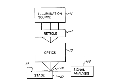
Fig. 1 generally illustrates a photolithographic system
utilizing the present invention. An illumination source 11
projects the image of a reticle 15 through optics 13 onto a
photosensitive resist covered wafer 12. The wafer 12 is placed
on an X-Y stage 10. A detector 14 is placed on the X-Y stage 10.
Apertures in the reticle 15 are matched to openings on the
detector 14. Detector 14 is moved so that the image of the
appropriate reticle pattern falls on the apertures in an opaque
layer. Signals from the detector 14 are interpreted by signal
analysis of the data in function box 114. The matched apertures
and openings provide desired imaging information, such as
alignment and position information as well as image quality
information.
Fig. 2 more clearly illustrates the top surface of the stage
10. Centrally positioned on the stage 10 is a wafer 12. The
CA 02234~32 1998-04-09
SVG-4016
detector 14 is preferably positioned in one corner of the stage
10. The stage is movable along X and Y axes permitting accurate
positioning of the detector 14.
Fig. 3 more clearly illustrates, but does not limit, the
structure of a detector according to the present invention. The
detector 14 is made up of a plurality of sub-detectors 16, 18,
and 20. Sub-detector 16 provides information relating to coarse
positioning. Sub-detector 18 provides information relating to
fine positioning. Sub-detector 20 provides information relating
to image quality. Sub-detector 16 is comprised of an exposed
detector array 34. The whole detector array could be a
conventional detector array such as a CCD or charge coupled
device. Other arrays that could be used are, for example a CMOS
array, a CMOS smart pixel array, and a photodiode array. This
requires adequate sensitivity at the wavelength the whole system
works at. Arrays such as CCD's or self scanned arrays are
available at the main wavelengths possible, 365, 248, and 193
nanometers. X-ray arrays are also available. An illumination
pattern 22, which is illustrated as an X-shape, but may be any
other predetermined shape, is projected onto the exposed detector
array 34. This illumination pattern is generated from an
aperture in a reticle or mask. The detector array 34 is able to
provide information relating to the general location of the
CA 02234~32 l998-04-09
SVG-4016
illumination pattern 22, thereby providing coarse positioning
information by standard pattern recognition techniques. The
coarse positioning information is used to obtain a fairly precise
location, to a few microns, of the detector 14 to facilitate the
positioning of the sub-detector 18 used in establishing fine
positioning information. The sub-detector 18 has an opaque
chrome layer 42 with openings 24, 24', 26, 26', 28, 28', 29 and
29' therein. The openings 24, 24', 26, 26', 28, 281, 29 and 29'
expose a portion of the detector array or photosensitive surface
or layer, such as a CCD or charge coupled device. Openings 24
and 24' are used to determine positioning in the X direction.
Openings 26 and 26' are used to determine positioning in the Y
direction. Openings 28, 28', 29 and 29' are skewed, in relation
to the X and Y movement of the stage 10, shown in Figs. 1 and 2,
and are used to obtain X and Y positioning information. The
longitudinal axis of openings 28, 281, 29 and 29' are preferably
skewed or offset 45~ from the X and Y axes of the stage 10, shown
in Figs. 1 and 2. The openings 28, 28', 29 and 29' permit the
detector of the present invention to be used with prior reticles
that utilize similarly shaped skewed alignment apertures. Sub-
detector 20 iS formed by openings 30, 31, and 32 formed in an
opaque chrome layer 42'. Opening 30 is used to obtain optimum
focusing information. Openings 31 and 32 are used to obtain
CA 02234~32 l998-04-09
SVG-4016
information relating to astigmatism. The openings 30, 31 and 32
in the opaque chrome layer 42' expose a photosensitive surface or
layer, such as a CCD or charged coupled device. The exposed
detector array 34 and the photosensitive surface or layer beneath
the opaque layers 42 and 42' are preferably made from a single
monolithic element. The detector 14 has openings 24, 24', 26,
261 28, 28', 29, 29', 30, 31, and 32 that are matched to
apertures formed in a reticle 15, shown in Fig. 1. By matched
it is meant that the dimensions of the aperture are related to
the dimensions of the openings such that the desired imaging
information is obtained and also each relevent opening is matched
to the element size of the array of detectors used. The
apertures formed in a reticle cause light from an illumination
source to be projected onto the openings 24, 24', 26, 26' 28,
281, 29, 29', 30, 31, and 32 in a predetermined way to establish
imaging information, such as positioning and image quality.
While only three sub-detectors 16, 18, and 20 have been
illustrated with respect to detector 14, it should be appreciated
that more than three sub-detectors 16, 18, and 20 may be formed
on a single monolithic photosensitive surface, such as a CCD or
charge coupled device. The application of an opaque chrome layer
42 or 42' to a portion of the photosensitive surface, and the
ease in which the openings are manufactured permits flexibility
CA 02234~32 1998-04-09
SVG-4016
and allows for multiple sub-detectors to be used. Additionally,
each sub-detector may have a plurality of similar openings
facilitating redundancy and signal averaging.
Fig. 4 more clearly illustrates a portion of the sub-
detector 18 and its operation. The rectangular openings 24 and
24' formed in the opaque chrome surface 42 expose a
photosensitive layer or surface 36 and 36'. The photosensitive
surfaces 36 and 36' produce an electrical signal when illuminated
by electromagnetic radiation from an illumination source. The
photosensitive surface is preferably formed in an array, for
example by a CCD or charge coupled device. The rectangular
openings 24 and 24' are separated by a distance d. A reticle or
mask having a matched or predetermined aperture creates an
illumination pattern 38 to be projected onto the sub-detector 18.
A portion of the illumination pattern 38 is caused to fall onto
the photosensitive surfaces 36 and 36'. The portion of the
illumination 38 falling onto the photosensitive surfaces 36 and
36' creates filled portions 40 and 40', respectively. The width
of the illumination 38 need only be greater than the distance d
between the openings 24 and 24', and less than the distance d
plus the combined width of the two openings 24 and 24'.
Therefore, the filled portions 40 and 40' could vary in width
creating different fill ratios. The precise positioning of a
CA 02234~32 1998-04-09
SVG-4016
reticle and stage on which the detector is mounted is easily
obtained by balancing the electrical signals generated by the
filled portions 40 and 40'. When the filled portions 40 and 40'
are equal, the illumination pattern 38 is precisely centered
between the openings 24 and 24'. Therefore, the reticle is
precisely positioned with reference to the detector, and
therefore the stage. This is accomplished without any scanning
and it may be done in a static environment without the need to
scan the detector and the reticle. Additionally, accurate
signals used for alignment are obtained with pulsed illumination
sources. A single pulse of illumination provides alignment
information. The circuitry needed to detect a balanced signal
generated from the filled portions 40 and 40' is relatively
simple and well known, and can be made very accurate. This
circuitry may be incorporated in the signal analysis 114,
illustrated in Fig. 1. The relatively simple and economical
structure also permits a plurality of similar openings in a
detector and apertures in a reticle to be formed, permitting
redundancy and averaging, which augments reliability and
accuracy. The position along a single axis can therefore very
accurately be obtained. By combining a plurality of openings and
apertures having intersecting or orthogonal axes, X and Y,
accurate alignment and positioning can very easily be obtained.
CA 02234~32 l998-04-09
SVG-4016
Noise levels and micro variations in position with time can be
determined by multiple time dispersed measurements
Fig. 5 is a cross section taken along line 4-4 in Fig. 4 and
illustrates the planar layered structure of the sub-detector 18.
The opaque chrome layer 42 iS formed on a silicon dioxide
protective layer 44. The requirements of opacity are not high as
the fill ratio is high. The protective layer 44 iS transparent
to the illumination and protects the photosensitive layer 46.
The photosensitive layer 46 iS formed on a substrate layer 48.
The layers 44, 46, and 48 are generally illustrative of a CCD or
charge coupled device which are commercially available. However,
on commercial devices, the protective layer 44 iS approximately 3
microns thick. This protective layer 44 may be reduced to 1
micron so that the opaque chrome layer 42 iS closer to the
photosensitive layer 46. This eliminates cross talk between the
elements of the detector array due to light spreading. Fig. 5
clearly illustrates the illumination pattern 38 and the filled
portions 40 and 40' illuminating the photosensitive layer 46.
Fig. 6 illustrates another portion of the sub-detector 18.
Fig. 6 more clearly illustrates the application of the present
invention to a different opening configuration. Openings 28,
28', 29 and 29' in the opaque chrome layer 421 expose the
photosensitive surface to electromagnetic illumination. Similar
CA 02234~32 l998-04-09
SVG-4016
matched or predetermined shaped apertures in a reticle form
illurnination patterns 138, 138', 139 and 139'. A portion of the
illumination patterns 138, 138', 139, and 139' illuminate the
photosensitive surface exposed by openings 28, 28', 29, and 29',
to form filled portions 140, 140', 141 and 141'. Analogous to the
embodiment illustrated in Fig. 4, the signals generated from the
filled portions 140, 140', 141, and 141' are balanced or made
equal so that precise alignment is obtained between the detector
14 affixed to the stage 10 and the reticle. The embodiment
illustrated in Fig. 6 has the advantage of being compatible with
existing reticles. Additionally, pairs of illumination patterns
138, 138', 139, and 139' are used with each pair of openings 140,
140', 141, and 141', respectfully. However, the illumination
pattern does not have to be divided, and may be a single pair of
illumination patterns, each spanning the distance between the
openings 28, 28', 29, and 291, respectfully.
Fig. 7 illustrates a reticle used to create the illumination
patterns illustrated in Figs. 4, 5, and 6. The apertures in the
reticle 15 are matched to the openings in detector 14. The
reticle or mask 15 is compr:ised of a sub-reticles 17, 19, and 21,
which correspond to the sub--detectors 16, 18, and 20, illustrated
in Fig. 3. Sub-reticle 17 has an X-shaped aperture 22' therein.
The aperture 22' forms the X-shaped illumination pattern 22
CA 02234~32 1998-04-09
SVG-4016
illustrated in Fig. 3. Sub-reticle 17 is used to obtain a
general or course alignment or position. Sub-reticle 19 has
apertures 38', 39', 238, 238', 239, and 239' therein. These
apertures 38', 39', 238, 238', 239, and 239' are of a
predetermined shape and location that are matched to the openings
in the sub-detector 18, illllstrated in Fig. 3. The apertures
38', 39', 238, 238', 239, 239' are projected or imaged onto the
sub-detector 18, illustrated in Fig. 3. The signals derived from
the illumination falling on the photosensitive layer are balanced
as explained with reference to Figs. 4, 5, and 6 in order to
obtain accurate position and alignment information. It should be
appreciated that when optics having a magnification are used, the
dimensions of the apertures in the reticle 15 are appropriately
proportioned in order to obtain the desired relationships for
obtain a signal providing position and alignment information.
For example, if reduction optics are used having a reduction
ratio of 4 to 1, the mask would be appropriately proportioned to
have predetermined sized apertures that are increased by a factor
of 4. Sub-reticle 21 has apertures 30', 31' and 32' therein with
predetermined positions and a shapes to match that of openings
30, 31, and 32 in sub-detect,or 20, illustrated in Fig. 3. The
apertures 30', 31', and 32' are imaged onto the openings 30, 31,
and 32 in sub-detector 20, illustrated in Fig. 3. The apertures
CA 02234~32 1998-04-09
SVG-4016
30' and 31' and 32' and openings 30, 31 and 32 are of a
predetermined shape and size or matched to provide image quality
information, such as focus and astigmatism. In this embodiment,
the apertures 30', 31' and 32 are sized so as to produce an image
whose isofocal intensity points matches the size of sub-detector
20. When imaged clearly or in focus the signal will be a
maximum. The reticle 15 may be made by any conventional reticle
manufacturing process, such as providing an opaque layer of
chrome on a glass substrate. The opaque layer of chrome is
etched to form the apertures therein by standard processing. The
embodiment of the patterned opaque layer over the detector may be
done by chrome coating the detector and patterning the layer by
E-beam techniques, as in standard reticle manufacture. This may
be done at the wafer stage of device fabrication. It is
anticipated that the surface of the detector will be made plane
to the accuracy required. Additionally, it should be appreciated
that the reticle 15 is only a small portion of a larger reticle
which will in general conta:in a circuit pattern thereon.
Figs. 8A and B illustrate how the focus image quality is
obtained. A relatively long, narrow rectangular opening 30 is
formed in the sub-detector :20, illustrated in Fig. 3. A matching
aperture 31 is formed in the sub-reticle 21, as illustrated in
Fig. 7, such that when in focus the image of the aperture 30' and
16
CA 02234~32 1998-04-09
SVG-4016
the edges of the opening 30 are coincident. Accordingly, when
the system is in optimum focus, a maximum signal is obtained, and
when the system is out of focus, a somewhat lesser signal is
obtained. This is illustrated in the graph of Fig. 8B. The in-
focus signal or optimum focus is illustrated as waveform 50
having a maximum signal amplitude. Waveform 52 illustrates the
signal when the system is out of focus, illustrating a lower
amplitude.
Figs. 9A and B illustrate an analogous technique to measure
astigmatism. Rectangular openings 31 and 32 have orthogonal
longitudinal axes, and are matched to predetermined size
apertures 31' and 32' in sub-reticle 21, illustrated in Fig. 7.
The apertures 31' and 32' a:re sized to provide an optimum or in-
focus image that is coincident with the edges of openings 31 and
32. Accordingly, when the system focus is zoomed in and out,
depending upon any astigmat:ism of the system, an optimal focus
along the X axes, corresponding to opening 32, and an optimal
focus along the Y axes, corresponding to opening 31, will be
obtained. This is illustrated in the graph of Fig. 9B, the X
axis of the graph represent:ing the focus and the Y axis of the
graph the signal amplitude. Waveform 54 represents the maximum
signal obtained from opening 32. The maximum point 58
corresponds to fx on the X axis of the graph. Similarly,
CA 02234~32 1998-04-09
SVG-4016
waveform 56 represents the signal from opening 31 corresponding
to fy on the Y axis of the graph. The distance between fxand fy
is representative of the astigmatism of the system.
While various shapes and functions have been illustrated in
the above embodiments, it should be appreciated that a variety of
shapes may easily be obtained to provide imaging information,
such as positioning and alignment information, as well as image
quality, on a single monolithic detector that is easily and
inexpensively manufactured. Additionally, it should be
appreciated that the present detector provides a plurality of
functions that can easily be changed or modified with little cost
as well as easily providing redundancy. A number of repetitive
openings may be used to provide redundancy in the event of a
failure of some of the elements. Additionally, the use of a
plurality or multiple repetitive openings permits signal
averaging to obtain a more :reliable information. Additionally,
the present invention permits positioning and alignment
information as well as image quality information to be obtained
with pulsed illumination sources or in systems that do not scan.
Accordingly, alignment information may be obtained for each
pulse of the illumination source, such as a pulsed laser. For
example, typically, a laser may pulse at 1000 Hz. This provides
an updated alignment signal every millisecond. Additionally,
CA 02234~32 1998-04-09
SVG-4016
variation or noise in the signal at steady state conditions is a
measure of vibration levels in the system. The accuracy of the
detector system depends upon the accuracy of the apertures and
openings. Typically, with the width of an opening of one micron
and approximately half the width being filled, 0.5 microns, by
the illumination pattern, would yield sensitivities of 2.5
nanometers with a typical commercially available CCD having
sensitivities in the order of 1%. This number may be varied by
adjusting the filled portion or fill ratio. A vernier
arrangement may be obtained by using multiple pairs of openings
that are offset from each other by a known amount or distance so
that a signal is obtained f:rom the multiplicity of the sets whose
most balanced sets supplies alignment information. Additionally,
different configurations may be used to measure other aspects of
image quality. For example, scatter may be approximated with the
use of a small sampling window, approximately one micron square,
that can be moved up to the line edge of an illumination pattern.
The signal varies with distance from the edge of the illumination
pattern, and its deviation from the diffraction limited
prediction may be used to monitor the scatter levels of a
lithographic tool. It is evident to one skilled in the art that
there are a multitude of reticle opening/opaque layer aperture
combinations that can exist to provide a multiplicity of
CA 02234~32 1998-04-09
SVG-4016
information on the image quality and position. Consequently,
there are detailed variances possible which will be clear to
those skilled in the art. Accordingly, although the preferred
embodiments have been illustrated and described, it will be
obvious to those skilled in the art that various modifications
may be made without departi:ng from the spirit and scope of this
invention, which i~ the use of matched pairs reticle : detector
apertures.