Note: Descriptions are shown in the official language in which they were submitted.
CA 02234673 1998-04-08
W O 97/15868 PCT~US96/OS828
FqLM CO~DYDSrrEFOR ELECTROSTAllC RECORDnNG
Field of the Invention
This invention relates to films that are capable of receiving images
directly deposited by electrostatic or electrographic processes and methods for
pl epa. ing such f Ims.
Back~round of the Invention
The terms "electrostatic" or "electrographic" are used generally
interçh~ng~?~hly for recording processes in which a recording head is utilized to
impose an electrostatic pattern upon a recording medium, and in which a toner
15 material is subsequently attracted to, and affixed to the electrostatic pattern.
Processes of this type are employed for p- ~p&l ing engine~oring graphics, a- Iwo- k for
adve, lisen-enLs, displays and the like.
In a typical electrostatic imaging process, a I t;coldillg head which
inr1ndes a linear array of a plurality of separately chal~eable electrodes, general1y
20 referred to as "nibs", is scanned acro,ss a recording medium, and the nibs are
selectively energized to impose an electrostatic pattern upon the m~rlillm The
charged medium is contacted with a toner, which typically comprises a liquid
co~ g a pigment or dye thereon. Excess toner is removed from the medium,
leaving toner only in the charged areas. The toner is subsequently dried or
25 otherwise fixed to produce a permanent image. The process can be utilized forsingle color or full color graphics and can be completed in a single pass across the
medium or in multiple passes across the m~tlinm
The recording medium is an important component of the
electrostatic im~ging system. The me-linm must be able to accept, retain, and
30 discharge the electrostatic pattern. The medium must also be co~ alible with the
toner system employed as well as the particular im~ing hardware, such as a single
or multiple pass electrostatic printer.
CA 02234673 1998-04-08
WO 97/15868 PCTAUS96/05828
Electrostatic printing of media conventionally requires the printing of
electrostatic images on a dielectric paper construction followed by ll~nsr~l- ofthat
image to polymer fi1ms. Such conventional electrostatic im~ing is disclosed in
U.S. Patent No. 5,1 14,520 (Wang et al.).
The diele~;ll ic paper construction typically comprises a paper or
paper-like substrate, a conductive layer coated on a major surface ofthe sul,~Ll~le, a
dielectric layer coated over the conductive layer, and a release layer coated above,
beneath, or with the dielectric layer to assure that the image received above the
dielectric layer can be transferred to the final substrate upon application of heat ~d
pressure. A commercially available example of this ll~n~rer process and the
products to accomplish that process is the ScotchprintrM Electronic Graphics
System available from Minnesota Mining and ~nufiqct1lring Company of St. Paul,
Minnesota.
Japanese Kokai Publication No. 3-69960 discloses a electrostatic
image recording adhesive sheet that can print electrostatic images directly. But this
publication does not disclose the composition of conductive coatings and dielectric
coatings sufficiently to achieve a commercial product capable of assured
reproducibility. In addition, it teaches that emulsion coatings should be employed
for polyvinyl chloride films, which tend to swell when brought into contact withorganic solvents.
Summary of the Invention
The art needs a process that can avoid the necessity of printing an
image on a temporary substrate and then tran~rt;lling that image to a permanent
substrate.
The art also needs a direct print film that can be used to produce
lasting, durable images on a permanent, durable substrate.
The art also needs a direct print film that can be plt;paled without
swelling the substrate but that permits the film to be collr~,l nlal~le.
One aspect of the present invention is the construction of a film for
the direct printing of electrostatic images.
CA 02234673 1998-04-08
WO 97/15868 PCT~US96/05828
In one aspect, the direct print film comprises a durable, conrc,llllal)le,
polymeric substrate having a conductive layer pre~,alt;d from a coating solutioncomprising conductive pigment and organic solvent.
"Durable" means the sul~ Les useful in the present invention are
S capable of u~ g the wear and tear associated with signage and may be used 2 to 5 years in exterior environments.
"Conrol nlable" means the substrates in a direct print film are capable
of co-3rol llling to uneven surfaces and I c~ ;n~ such collrc l l-laLion during use
without significant force applied per unit area of the film. Typically the
10 conformable substrate can be adhered with hand pressure and conrc,llll to a surface
having periodic or compound irregularities, such as a rivet or welded ridge on the
exterior metallic surface of a tractor trailer, without the substrate lifting from the
surface.Preferably, a conformable substrate in a direct print film exhibits a yield
point and/or permanent strain when subjected to a maximum tensile stress of about
3.5 X 10⁷N/m2 (5000 lbs./square inch) at room temperature according to ASTM
D638-94b (1994), when the caliper used for the test in~ludes the total cross-
sectional thickness of the substrate, the thickness of the adhesive, and the
thiçknesses of the conductive layer and dielectric layer.
ln another aspect, the direct print film comprises a vinyl-co..~ ;..g
polymeric substrate having a conductive layer coated thereon from organic solvent,
wherein the conductive layer comprises a carboxylated acrylic binder and a
conductive pigment comprising antimony and tin oxide.
In another aspect, the direct print film comprises a durable,
conformable, polymeric substrate having on a major surface a conductive layer
coated thereon from an organic solvent, and a dielectric layer coated on the
conductive layer, wherein the conductive layer comprises a conductive pigment
comprising intim~tçly mixed antimony and tin oxide.
Preferably, the conductive pigment in the conductive layer has a bulk
powder resistivity ranging from about 2 to about 15 Ohm-cm.
"Bulk powder resistivity" means electrical resistivity of the bulk
powder used in the conductive pigment according to the following test described by
CA 02234673 1998-04-08
W O 97/15868 PCT~US96/0~828
E.I. DuPont. one of the commercial suppliers of conductive pigments. As described
in Capano et al., "The Application of ZELEC ECP in Static Dis~ ative Systems"
(Du Pont Chemicals, Deepwater, New Jersey September 1992), a cylindrical cell,
with electrodes at the top and bottom is used to make bulk powder resistivity
5 measurements. A weighed amount of powder is placed into the cell and then
pressed with a laboratory press into a pellet. The ~ nce between the two
electrodes is then measured as a function of the pressure applied and the Ihicl~l~ess
of powder pellet. The bulk powder resistivities of Du Pont conductive pi~m.?nt~
commonly range from about 2 Ohm-cm to about 20 Ohm-cm accol di-~g to th~s test.
10 Another supplier of conductive pigm~ntc, Goldschmidt A.G. of Essen, Gerrnany,identifies bulk powder resistivity as "specific resistan~e" and employs a test method
available from Esprit Chemical Company of Rockland, Maryland. For purposes of
this application. the property of"bulk powder resistivity'~ includes the conce,ol of
the property of"specific re~ict~n~-e".
In another aspect, the direct print film Culllyl ises a durable,
conrullllable, polymeric substrate having on a major surface a conductive layer
coated thereon, and a dielectric layer coated on the conductive layer, wherein the
dielectric layer incl~ldes spacer particles and abrasive particles. Spacer particles,
which are generally of a lower hardness than abrasive particles and/or have a more
rounded configuration than abrasive particles, function to provide a rollghnç~c that
n,~ S a relatively small gap between the im~ging head of the electrostatic printer
and the rçm~ining surface of the direct print film. Abrasive particles function to
provide abrasivity to contact the im~ging head of the electrostatic printer in order to
clean oxidation and other unwanted debris from the imaging head.
Optionally, the direct print film has a field of pressure sensitive
adhesive coated on the other major surface of the direct print film, protected by a
release liner. The field of pressure sensitive adhesive permits the direct application
of the film having an image printed thereon to be adhered to a final location.
Another aspect ofthe invention is a method for p-~palillg
elecLlc,sl~lic print film.
CA 02234673 l99X - 04 - 08
WO 97/lS868 PCT/US96/05828
A feature of the present invention is the ability to directly print
electrostatic images on film of the present invention while concurrently ~ g
the imaging heads in an acceptable condition.
Another feature of the invention is ease of construction of a direct
5 print film.
An advantage of the present invention is the ability to ~ e
m~ntlf~r~turing steps for the preparation of electrostatic images on a final substrate.
Another advantage of the present invention is the ability to provide
for electrostatic direct printing a film that has a surface resistance in its conductive
layer of about 2 x ] o5 to about 3 x 1 o6 Ohms/O and that has a surface rPci~t~nce in
its dielectric layer of greater than about I x I o8 Ohms/O . This difference in surface
resistance results in clear, crisp images generated by the electrostatic printer.
"Surface Resistance" is the measure of D-C reCi~t~nce of
moderately conductive materia]s according to ASTM Test Designations D 4496-87
and D 257-93 and is important to films of the present invention to characterize
electrical performance of the conductive ]ayer of the present invention, which layer
functions as the ground plane of the capacitQr, that is being formed by the direct
print film of the present invention during electrostatic printing.
Another advantage of the present invention is the ability to provide a
direct print film where the conductive layer and the dielectric layer are both
compatible with the substrate.
Another advantage o~the present invention is the ability to provide a
direct print film that when imaged can provide an average color density of from
about 1.2 to about 1.5 optical density units using a reflection densitometer.
"Color Density" is the measure of the intensity of the individual
primary colors produced by the electrostatic printer on the recording medium to
forrn the latent image and is important to films of the present invention because
color density has a major impact upon the perceived aesthetics of the image on the
recording me-lium produced electrostatically.
Another advantage of the present invention is that the direct print
film of the present invention provides a durable image.
CA 02234673 1998-04-08
W O 97/15868PCT~US96/05828
Embo-liment~ of the invention are described in relation to the
following drawings.
Brief Description of the Drawings
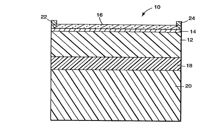
5Fig. 1 is a cross-sectional view of the film of the present invention.
Embodiments of the Invention
Referring to Fig. 1. a typical construction of a film of the present
invention 10 col,lplises a substrate film 12 having on a major surface thereof, a
10 conductive layer 14 and a dielectric layer 16. On the opposite major surface of film
substrate 12 resides optional pressure sensitive adhesive 18 protected by a release
liner 20.
Substrates
5Substrates are preferably a durable material that resists any swelling
or other loss of continuity when coated with the conductive layer and also resists
deleterious effects of exterior signing environments in~ 1ing large ambient
temperature ranges -60~C to + 107~C direct exposure to sun and is also
co"~""able for fixing to exterior surfaces wherein it may be adhered over surfaces
20 with some compound curvature or non unifo""iLy e.g. walls or surfaces with screw
heads or rivets slightly proud of the surface without easily ripping the material or
tenting . However in some aspects of the invention the substrate need not be
limited to these durable co"ro""able substrates. A less durable plastic is useful for
interior signing applications.
Substrates can be clear tr~n.sluc.ont or opaque depending on the
application of the invention. Opaque sub~ les are useful for viewing an image
from the image side of the printed sheet in lighting conditions such as artificial
lighting or sl~nlight. Tr~n~luc~nt substrates are particularly useful for backlit
usages, for example a luminous sign.
Substrates useful in the practice of the present invention are
conlmt;l~;ally available and many are designed to be exterior durable which is
--6--
CA 02234673 1998-04-08
WO 97/15868 PcT/u~~~l'7828
preferred. Nonlimiting examples of such sub~ es include ScotchcalTM Marking
Fitms and ScotchcalTM Series 9000 Short-Term Removable (STR~ Film available
from 3M Company, AveryTM GLTM Series Long Life Films, AveryTM XLTM Series
Long Life Films, AveryTM SXTM Series Long Life Films, suitable films from the
5 FasCalTM or FasFlexTM range of films or any other suitable marking, graphic orpromotional films available from Fasson, Avery or Meyercord. However, other
m~mlf~ctllrers of suitable materials exist and the invention shall not be limited to the
above. Almost any material composed of a plastic sheet could be used depending
on the use of the final image, for example, whether outdoor durability is required,
10 and providing that the conductive layer can adhere to the film surface sufflciently
well.
Useful substrates can have a variety of surface finishes such a matte
finish as provided with ScotchcalTM Series 9000 Short-Term Removable (STR)
Film or glossy finish as provided with ScotchcalTM 3650 Marking Film. Plastic films
15 can be extruded, calendared or cast dirr~, ~"L plastic materials may be used, such as
those exemplified by the ScotchcalTM plasticized poly(vinyl chloride) or Surlyn, an
ionomer. Any suitable plastic material can be employed. Nonlimitin?~ e,~all"~lesinclude polyester materials exemplified by MylarTM available from E.I. Du Pont de
Nemours & Company, MelinexTM available from Imperial Chemicals, Inc., and
20 CelanarTM available from Celanese Corporation. P, ere" ~d materials for substrates
can include those that are plasticized poly(vinyl chloride)s or ionomers although the
invention is not limited to these. Pl erel, ed materials are white opaque or
tr~n.CI-Icent materials but transparent materials and colored opaque, tr~ncluc.?nt or
ll~n~.~a~enL materials could be useful in special applications.
Typical thic~necs~s ofthe substrate are in the range of 0.05 to 0.7~
mm. However, the thickness can be outside this range and almost any thickness can
be useful provided the film resists tearing or splitting during the printing andapplication process. Given all considerations, any thiÇ~ness is useful provided the
substrate is not too thick to feed into an electrostatic printer of choice.
.
-
CA 02234673 1998 - 04 - OX
WO 97/15868 PCT/US96/05828
Conductive Layer
For electrostatic im~ging on film 10, a conductive coating layer 14 is
provided from an organic solvent-based conductive coating so1ution on the upper
major surface of film substrate 12. In direct conl-~:,l to the te~ehing ofthe Jal-Al-~se
Kokai Publication No. 3-69960 described above, the organic solvent-based
conductive coating solution does not swell col~ol--lable substrates used in the
present invention. Furthermore, conductive coating solutions employing organic
solvents are used to assure that the conductive layer has good ply adhesion with the
conro- ~--able substrate surface. Also, use of organic solvents in the conductive
coating solutions permit the conro----able substrate to avoid any pl;llUII~, of its upper
major surface to receive the conductive layer. Better wettability can be achieved on
an unprimed substrate, to avoid foaming caused by aqueous based coating
solutions.
The conductive coating layer can be electronically conductive or
ionically conductive. Electronically conductive layers employ a plurality of particles
of a transparent~ electrically conductive material such as antimony doped tin oxide
or the like, disposed in a polymeric matrix.
Attributes of conductive layer 14 include adhesion to film substrate
12, deposition using a suitable solvent system, and moisture inc~n.citivity after the
layer 14 is dried on substrate 12.
When an electrically conductive layer is desired, conductive layer l 4
is prepared from a solution of a conductive formulation that generally comprises a
binder, conductive pi~ment.c7 dispersant, and organic-based solvent, the latter of
which is removed during the m~n~lf~ctllring process.
The weight percent of solids to organic solvent in the conductive
formulation can range from about 10 to about 40, with about 25 weight percent
being pl esen~ p. e;re. . ~d for ease of application to film substrate 12.
After coating of conductive formulation on film substrate 12 and
evaporatlon or other removal of organic solvent, the thickness or caliper of theconductive layer 14 can range from about 2 to about 5 ~lm with about 3 llm being se~ y ~ t r~ d.
_ _ _ _ , , ,
CA 02234673 l99X-04-08
W O 97/1~868 PCT~US96/05828
As stated above, the conductive layer 14 should have a surface
resistance ranging from about 0.2 to about 3 megaohms per square. This level of
surface resistance provides the proper level of conductivity to form the ground
plane for the direct print film of the present invention.
Non-limiting ex~mrles of binders include acrylics, polyester, and
vinyl binders. Among acrylic binders, carboxylated acrylate binders and
hydroxylated acrylate binders are useful for the present invention, such as those
commercially available from Allied Colloids of Suffolk, VA such as "Surcol SP2"
carboxylated acrylate binder and "Surcol SP5 hydroxylated acrylate binder. Amongsome of the polyesters materials which can be employed as binders are materials
sold by Goodyear of Akron, Ohio under the brand "Vitel", of which grades PE222
and PE200 are particularly suitable for use in the present invention. Also vinylresins such as "UCAR" "VAGD" brand resins from Union Carbide of Danbury,
Connecticut can also be useful.
Conductive pigment~ can include antimony-co.l~ g tin oxide
pigments or other pi~mentc such as indium doped tin oxide, c~iminm st~nn~te, zinc
oxides, and the like.
Non-limiting e~ ,les of antimony-co..~ -g tin oxide conductive
pigments include those pigments disclosed in U.S. Pat. No. 5,192,613 (Work, III et
al.); U.S. Pat. No. 4,431,764 (Yoshizumi); U.S. Pat. No. 4,965,137 (Ruf); U.S. Pat.
No. 5,269,970 (Ruf et al.); and in product literature for "Tego S" pigm~nt.c
commercially available from Gol~l~chmidt AG of Essen, Federal Republic of
Germany and "Zelec" pigments commercially available from DuPont of Wilmington,
Delaware. When the Goldschmidt Tego S conductive pigment is employed, its
particle size should be reduced by a milling process.
Particle size ofthe conductive pigments in the conductive layer 14
can range from about 0.02 to about 10 ~lm. Below about 0.02 ~m particle size, the
conductive pigment is too easily imbibed with solvent action, whereas at greaterthan 10~m, the coating of dielectric layer 16 on the conductive layer 14 limits
protrusion ofthe conductive pigment particles into the dielectric layer 16.
CA 02234673 1998-04-OX
WO 97/15868 PCT~US961~5828
Preferably, the average particle size can range from about 0.5 ~lm to
about 4 ~lm, with particles of about I ~Lm being most pl ~re., ~d.
The bulk powder resistivity can range from about 2 to about 15
Ohm-cm with about 2 to about l 0 Ohm-cm being p ~r~ d and about 6 to about 7
Ohm-cm being p-t;sel-lly p-c:re-lt:d. With the DuPont p;g~ , the bulk powder
resistivity can be about 2-5 Ohm-cm for"Zelec 3410-T" pignlents and 4-1~ Ohm-
cm for "Zelec 261 0-S" found acceptable for the present invention. The bulk
powder resisitivity has been found to be important in controlling the final
appearance of the image on the direct print film because materials that are too
10 resistive require the use of a larger amount of conductive pigment can cause an
objectionable amount of background color in the final image.
The "Tego S" particles are identified to have a specific reci~t~nce of
10, which is believed to compute to about bulk powder resistivity of about 10.
The present invention preferably uses antimony-co~ pigments
15 which have antimony intim~tely mixed with tin oxide, that is, present in the forrn of
an antimony and tin oxide coating on silicon co..li1;..;..g particles (believed to be
typified by the DuPont materials and disclosed in the Work III, et al. patent
identified above) or in the form of antimony doped through a lattice of tin oxide
particles (believed to be typified by the Tego materials and disclosed in the Ruf and
20 Ruf et al. patents identified above), as colll~oal c;d with antimony - tin oxide reacted
materials (believed to be typified by the Mitsubishi materials described in Yoshizumi
patent identified above). While not being limited to a particular theory, better bulk
powder resistivity within the acceptable range is achieved by antimony and tin oxide
co~ting~ or antimony doped into tin oxide lattices that create ''~ ely mixed"
25 antimony with tin oxide, as opposed to particles of antimony reacted with tin oxide.
A variety of surfactant materials can be employed as di~ al-L~ for
the conductive layer ]4 in the present invention, incl--ding nonionic and anionic
dispersants. In general, anionic di~l,e-~a-lLs are most plerellt;d, although theinvention is not limited thereto. One particularly ple~--ed anionic dispersant is a
30 material branded "Lactimon'~ dispersant from BYK-Chemie USA Corporation of
-10-
CA 02234673 1998-04-08
W O 97115868 PCT~US9'J ~28
Wallingford, Connectic-lt. Also co~ el ~,ially available from BYK-Chemie USA
Corporation is a nonionic dispersant is branded "Anti Terra U" dispersant.
Non-limiting e~alnples of solvents for the conductive forrnulation
include ethyl acetate and ethanol.
Forrnulations of the conductive layer 14 require a weight ratio from
about 5:1 to about 1:1 of pigment:binder with a p~ lce of a weight ratio of 3:1
pigment:binder. When "Tego S" conductive pigl,le,~l is employed, the weight ratio
can range from about 3.0:1 to about 4.7:1 pigment: binder. When the DuPont
"Zelec" conductive pigment is employed, the weight ratio can range from about 1:1
to about 4:1 pigment:binder.
When the pigment to binder ratio falls below 1:1, there is in~ieq~l~te
bulk conductivity of layer 14. When the weight ratio of pigment:binder exceeds
about 5:1, there is insufficient cohesive ~llen~lh ofthe layer 14 on film substrate 12.
Dielectric I_ayer
Dielectric layer 16 can be coated on conductive layer 14 to provide
the electrostatic c~p~cit~nce required for electrostatic im~gin~
The dielectric layer 16 is of relatively high electrical resistivity and
contributes to the pe,ro""ance of fflm 10 for direct printing of images
electrostatically. In addition to providing the interface of film 10 with the I eco~d;"g
head and toner, dielectric layer 16 covers and protects conductive layer 14 and
provides the top surface for film 10.
A variety of im~ging defects can be attributed to incorrect properties
of a dielectric layer in electrostatic or electrographic im~ging processes. Dielectric
2~ layer 16 is constructed to ~ jm~in~ defects. Some of the noted defects
include image flare, which results from unwanted electrostatic discharge within the
recording medium; image drop out, which occurs when a portion of the image is not
printed onto the medillm; and shorting between nibs on the im~ging head because
the head is not kept sufficiently clean by a dielectric layer of passing recording
mP~ m past the nibs over time.
CA 02234673 l99X-04-08
WO 97/15868 PCTrUS96/0~828
Dielectric layer 16 is coated on layer 14 from a dielectric formulation
that comprises particulate matter of both spacer particles and abrasive particles,
preferably in particular ratios dispersed in a binder.
Both the spacer particles and the abrasive particles should be
5 selected with consideration to the refractive index thereof, so as to provide index
m~t~.hing to the r~m~in~er of dielectric layer 16 and filîn 10. In this manner, film 10
has a uniform appearance. This is especially so when ll~n~l.alel.l products are
desired. In the case of opaque products, a uniform appec.. ~nce would not ~e
critical.
The spacer particles can be fabricated ~rom a material having
sufflcient rigidity to with~t~n~l coating and h~ndling, but need not be highly
abrasive. Nonlimiting examples of materials useful as spacer particles include
relatively soft materials such as a polymer or a mineral such c~lr.il-m carbonate or
relatively hard materials such as silica or glass, provided that such relatively hard
15 materials have a relatively rounded configuration. More particularly, useful spacer
particles can be made from synthetic silicas, glass micro beads, natural minerals
(e.g., calcium carbonate), polymeric materials such as polypropylene,
polycarbonate, fluorocarbons or the like.
Typically spacer particles have an average size ranging from about 1
20 to about 15 ~lm, and pl are, ~bly below about 10 ~lm. In general, spacer particles will
be present in a distribution of sizes, although it is most pl c~r~l ~ ad that the particles
remain in a size range of about 3-10 ~lm.
One particularly pl cre~ ed group of spacer particle materials
comprise amorphous silica, of which is most pl ~re. . ad the synthetic, amorphous
25 silicas sold by the W.R. Grace Corporation under the brand "Syloid 74". Thesematerials havean average particle size of appl u~cilllalely 3.5-7.5 ~Lm as measured on
a Cûulter appalz~ s and an average particle size of 6-10 ~m as measured on a
Malvern analyzer. One specific member of this group of materials comprises ~,"Syloid 74 X-Regular" particles which have an average particle size of 6.0 as
30 measured on a Coulter appal,lLus.
-12-
CA 02234673 1998-04-08
WO 97/15868 PCT~US96/05828
Abrasive particles useful for dielectric layer 16 of the present
invention are provided to assure that the pt~ ance of spacer particles and
abrasive are effectively decoupled so as to provide an optimized dielectric m~ lm
The abrasive particles will generally be harder than the spacer
5 particle material chosen and will usually have a more irregular configuration or
texture than the spacer particle material. Among some of the p-~;fl~lled abrasive
materials are silica materials such as microcrystalline silica and other mined or
processed silicas, as well as other abrasives such as carbides and the like
The abrasive particles generally have the same size ran~2:e as the
10 spacer particles, typically in the range of about I to about 15 ~lm and p~erel~bly less
than 10 llm.
One particularly pl~relled group of abrasive materials con,plises
mined, microcrystalline silica sold under the brand "Imsil" by Unimin Specialty
Minerals, Inc. of Elko, Illinois. These materials colnpl ise 98.9% silica with minor
15 amounts of metal oxides. One grade having particular utility comprises "lmsil A-
10" which has a median particle size of 2.2 llm, and range of particle sizes such that
99% of the particles have a size less than 1 0~1m and 76% of the particles have a size
of less than S~lm.
The proportion of spacer particles to abrasive particles are such that
20 the spacer particles are present in a larger amount. Preferably, the ratios of spacer
to abrasive particles fall within the range of about 1.5:1 to about 5:1. Most
pl el~, ~bly, the ratio of spacer to abrasive particles is approximately 3 :1.
The spacer particles and abrasive particles are disposed is a binder
which generally comprises a polymeric resin. The resin should be of fairly high
25 electrical resistivity, and should be compatible with both types of particles and the
toner. The resin should have sufficient durability and flexibility to permit it to
function in the electrostatic im~ging process and should be stable in ambient
atmospheric conditions.
There are large number of resins that meet these criteria. One
30 ~ rt;l . ed group of materials are the acrylic copolymers of the type commercially
,
CA 02234673 l99X-04-08
WO 97/15868 PCT~US96/05828
available from Rohm and Haas of Philadelphia, Pennsylvania under the brand
"Desograph-E342-R" .
A coating mixture to prepare dielectric layer 16 can employ solvents
such toluene into which the binder, spacer particles, and abrasive particles can be
S added as solids. The range of total solids in the coating mixture cân be from 10 to
about 35 and preferably about 15 to 25 weight percent ofthe total coating mixture.
Of the total solids, the binder solids can comprise from about 93 to about 78 and
", I;rt . ably 82 weight percent. Of the total solids, the particles solids ~pl efe. ~bly in a
3: I spacer:abrasive mixture) can comprise from about 7 to about 22 and pl-erel~ly
18 weight percent.
The particle solids for the coating mixture can be blended by ball
milling for approximately two hours at room tel"pe~ re. Under these conditions,
there is no significant reduction in particle morphology, and the ball milling process
only serves to mix and disperse the particles. Other processes could be employed.
Surface rol~ghnçcs is desired to provide topography for deposition of
toner particles is based on a Sheffleld method measurement described in TAPPI
Test T 538 om-88 published by the Technical Association of the Pulp and Paper
Industry of Atlanta, Georgia.
The dielectric layer 16 can have a surface rou~hne~s ranging from
about 50 to about 200 Sheffield units and pl t;rt;.ably from about 80 to about 180
with 140 being presently pi ~rt;" ed.
.OptiQnal Pressure Sensitive Adhçsive -- -
Any conventional pressure sensitive adhesive used for the
construction of image graphic films can be used with the films 10 of the presentinvention. The field 18 of the p, ~s~ul ~ sensitive adhesive can be coated on film
substrate 12 prior to, or contemporaneous with, construction of the film 10 of the
present invention.
Non-limiting examples of pressure sensitive adhesives useful with the
present invention include those adhesives described in U.S. Pat. Nos. Re~ 24,906(Ulrich); 2,973,826; Re. 33,353; 3,389,827;4,112,213; 4,310,509; 4,323,557;
-14-
CA 02234673 1998-04-08
WO 97/1~868 PCT~US96/05828
4,732,808; 4,917,929; 5,141,790 (Calhoun et al.); 5,229,207 (Paquette et al.); and
5,296,277 (Wilson et al.) and European Publication 0 051 935. A p-ese"lly
p.t;rel-ed adhesive is an acrylate copolymer pressure sensitive adhesive formed from
a 90/10 weight percent monomer ratio of 2-methylbutyl acrylate/acrylic acid in a65/35 heptane/~cetone solvent system (39-41% solids) and having an inherent
viscosity of about 0.7-0.85 dl/g.
A line of commercially available film substrate with an optional
pressure sensitive adhesive of those described above is ScotchealTM Marking Films,
especially ScotchcalTM 3650 Marking Films. Thus, one ean construct direct print
films ofthe present invention from t,hese comlnel~ially available films with theaddition of the conductive and dielectric layers described above.
Thickness of adhesive l8 can range from about 0.012 mm to about
I mm with a thickness of about 0.02~ mm (I mil) being plc;rt;lled.
Optional Liner
Liner 20 can be constructed from any conventiona1 release liner
known to those skilled in the art for image graphic media. Non-limiting examplesinclude PolyslikTM release liners colllule-c;ally available from Rexam Release of Oak
Brook, Illinois and polyester liners such as a 0.096 mm polyethylene te~pl-lhAl~te
film with a matte b~kside coating on one major surface and on the other major
surface, a v~n~rlil~m oxide/surfactant/sulfopolyester ~ntict~tic primer coating and a
con~lçnc~tion cure silicone exterior coating. These ~ntict~tic coatings are generally
described in U.S. Pat. No. 5,427,835 (Morrison et al.).
Conductivç Groundin~ Stripe
Referring again to Fig. 1., a pair of electroconductive ground stripes
22 and 24 can be provided in order to aid in the prevention of"leading edge fog" by
providing an avenue for residual charge to be elimin~ted from the ground plane.
These stripes 22 and 24 ranging from about 0.76 to about 2.54 mm ~,vide are applied
to dielectric layer 16 at opposing lateral edges of film 10.
CA 02234673 1998-04-OX
W O 97/15868 PCT~US96/05828
Stripes 22 and 24 can be made from a conductive ink sold under the
brand "Multifilm, Conductive Black Ink 9093E20r' from Raffi and Swanson of
WilmingtQn, ~cs~chl-~ettc and are configured to permeate dielectric layer 16 at
such lateral edges of film in order to provide an electrical ground to the conductive
5 layer 12.
Thus, a film 10 of the present invention can have in sequenti~l order,
a release liner 20 comprising from about 0.07 to about 0.15 mm (about 3 to about 6
mils) thickness, a field of pressure sensitive adhesive 18 co~ isillg about 0.03 mm
(about 1 mil) thickness, a film substrate 12 CO"~ g from about 0.05 to about
0.10 mm (about 2 to about 4 mils) thickness, a conductive coating layer 14
COl~l~" ishlg from about I to about S micrometers (0.04-0.2 mils), a dielectric layer
16 comprising from about 2 to about 4 micrometers (0.08-0.16 mils) thickness, and
a pair of electroconductive ground stripes 22 and 24 at lateral edges of film 10 that
permeate layer 16 to layer 14.
Method of Formin~ Films of the Present Invention
A pl ~re" ed method of constructing films of the present invention
comprises a modular construction, but can comprise a sequential construction. Inthe sequential construction, beginning with release liner 20, each of the layers 18,
16, 14 and 12 are built on top of release liner 20.
Preferably, the method of the present invention employs a modular
construction wherein the first step is the casting of a film organosol onto a
temporary release liner, followed by fusing the organosol to form a substrate 12according to techniques known to those skilled in the art. In an independent
module, the field of pressure sensitive adhesive 18 is cast on release liner 20
according to techniques to those skilled in the art. Then, the module of film
substrate 12 on the temporary liner is joined with the module of field of pressure
sensitive adhesive 18 on liner 18 and the temporary liner is discarded.
Alternatively, one can employ a conll"elcially available pressure
sensitive adhesive-backed polymeric film in substitution for the above describedmodular construction.
-
CA 02234673 1998-04-08
WO 97/15868 PCT/U',-'~3&~8
Conductive layer 14 can be coated on film substrate 12 using any
technique known to those skilled in the art, preferably a wire bar coating technique
as known to those skilled in the art. The # wire bar of from about 6 to about 40 is
used to achieve the 1-5 micrometer thiçl~n~oss described as suitable for layer 14, with
a #10 wire bar being useful for DuPont conductive particles and a #12 to #40 wire
bar being useful for Tego conductive particles. The wire bar coating process step
can operate at a line speed ranging from about 9 meters per minute to about 19
meters per minute and preferably about 12 meters per minute (40 feet per minute).
Dielectric layer 16 is coated on conductive layer 14 according to
coating techniques known to those skilled in the art, p,efel~bly a reverse gravure
coating of the dielectric layer 16 onto conductive layer 14. In those in.et~nces where
a wire bar is l-tili7etl, the total solids are preferably about 16 weight percent. Where
a reverse gravure process is employed, the total solids are preferably about 25
weight percent. The ruling mill cylinder having a theoretical "lay down" factor of
about 0.031 mm to about 0.078 mm is used to achieve the I .5-5 micrometer
thickness described as suitable for layer 16 with 3 micrometer thickness being
p, ~rt;" ~d. The reverse gravure coating process step can operate at a line speed
ranging from about 1.5 to about 62 meters per minute, and preferably about 15
meters per minute. The reverse gravure can operate at a roll ratio ranging from
about 0.5 to about 1.5, and preferably about 1Ø
When ground stripes 22 and 24 are employed, such stripes can be
applied to lateral edges of film 10 using teçhniquee known to those skilled in the art,
pl ~;rel ~Iy an offset gravure or flexographic coating of stripes 22 and 24. Stripes 22
and 24 permeate layer 16 at such lateral edges to create a ground path from stripes
22 and 24 to layer 14. The offset gravure or flexographic coating process step can
operate at a line speed ranging from about 12 meter per minute to about 31 meters
per minute, and preferably about 15 meters per minute ~50 feet per minute~.
After im~ging, film 10 can be protected with overl~ films.
L Nonl;---;l il~O examples of overl~min~te films suitable for use with films 10 of the
present invention include Scotchprint~M Nos. 8910 and 8912 films commercially
available from the Com,l,el~,ial Graphics Division of 3M Company.
,
CA 02234673 1998-04-08
WO 97/15868 PCT~US96/05828
Usefulness of the Invention
The ability to provide a direct ~lillLil~g of an electrostatically printed
image on a durable film substrate opens a wide variety of opportunities to one
5 skilled in the art of electrostatic printing using digital im~gjng te~hniq-~esOne can e~ e the necessity of using an non-durable, temporary
substrate for ll~n~rel to a durable film substrate via a heatlpressure lA~n;~ ;on
accordillg to the processes described in U.S. Pat. Nos. 5,114,520 (Wang et al.) and
5,262,259 (Chou et al).
The films ofthe present invention are conrol.l,able due to the
conformable nature of the substrates selected and the conformable adhesive layercont~ting one major surface of the substrate and the conrol ll,al~le conductive and
dielectric layers contacting the opposite major surface of the substrate. Preferably,
a conformable substrate in a direct print film exhibits a yield point and/or p~, Illan~,.lL
strain when subjected to a maximum tensile stress of about 3.5 X 10⁷N/m2 (2000
Ibs./square inch) at room telllpél~.lure according to ASTM D638-94b (1994), whenthe caliper used for the test includes the total cross-sectional thicknecs of the
substrate, the thickness of the adhesive, and the thiç~nesses of the conductive layer
and dielectric layer. More plefel~bly, the maximum tensile stress limit is about 1.4
X 107 N/m2 to provide more ~o.lr~JIlllable films. Most preferably, the maximum
tensile stress limit is about 7 X 10⁶ N/m2 to provide even more confo,lllable films.
Conformability ofthe films still require internal integrity. Desirably, the minimllm
tensile stress limit is about 6.9 X 10⁴ N/m2 {l0 Ibs./square inch) and pleÇel~Iy the
minimllm tensile stress limit is about 1.7 X 10⁵ N/m2 (25 Ibs./square inch)
Films 10 of the present invention can provide an average color
density as measured according to a "Reflective Optical Density of a Status T
Method" under the requil~ t;n~s of ANSI/ISO 5/3-1984, ANSI PH2. 18-1985
published by the Graphic Communications Association of Arlington, Virginia of
from about 1.0 to about 1.6 O.D. Units. Preferably~ the average color density
ranges from about 1.3 to about 1.5 O.D. Units. These values show that films 10 of
the present invention has an excellent color im~ging capability after electrostatic
-
CA 02234673 l998-04-08
W O 97/15868 PCT~US96/05828
printing directly onto film 10 using electrostatic printers otherwise used for the
processes described in Wang et al. and Chou et al. above.
Films 10 of the present invention can provide a Base Color Shift as
evaluated using a Hunter Colorspace measuring colorimeter of from about -2 to
S about -7 Dalklless/Lightness Units as compared to ScotchcalTM 3650 Marking Fi1m
commercially available from 3M Company. This color shift is intended to show
how little difference in relative whiteness the films 10 of the present invention differ
from a commercially available marking film that is useful in the heat/plt~ult;
;( n step of the Wang et al. or Chou et al. processes.
Films 10 of the present invention can provide a 60~ Gloss from about
2 to about 30, with about 7 being ~ relled. 60~ Gloss can be measured as
described in ASTM D2457-90 (1990).
For an appreciation of the scope of the present invention, the
e,~amplcs and testing methods follow.
Testin~ Methods
Bulk Powder Resistivity: "The Application of ZELEC ECP in Static
Dissipative Systems" (Du Pont Chemicals, Deepwater, New Jersey September
1992)
Specific Resict~nce: "Tego Conduct S Resisitivity Measurement and
Apparatus" (available from Esprit Chemical Company, Rockland, Maryland)
Surface ~ecict~nce: ASTM D 4496- 87 and ASTM D 257- 93
published by American Society for Testing and Materials.
Color Shift: ASTM D 2244 - 93 published by American Society for
Testing and Materials.
Color Density: "Reflective Optical Density on a Status T Method" "
under the requirements of ANSI/ISO 5/3-1984, ANSI PH2. 18-1985 published by
the Graphic Communications Association of Arlington, Virginia.
Sheffield: Sheffield method measurement described in TAPPI Test T
538 om-88 published by the Technical Association ofthe Pulp and Paper Industry
of Atlanta, Georgia.
-19-
CA 02234673 1998-04-08
WO 97/15868 PCTAUS96/05828
Exa~ les
The coating mixtures for the conductive layer is p,~paled for all of
5 the examples accordi~ to details below and identified in Table 1, subject to the
following common techniql~çs employed.
Example 1 was plepaled by mixing 85 parts ethanol, 35 parts ethyl
acetate, 45 parts of Surcol SP-2 binder at 50% total solids until a clear solution was
achieved. Then with good ~git~tion, 14 parts of Zelec ECP 2601-S particles
10 (silicon dioxide core with antimony doped tin oxide coating) was slowly added,
followed by stin ing for more than one hour. Then the solution was 1, all~rel, ed to a
"Kady Mill" and milled for 30 minutes. The coating solution was applied to
unprimed polyvinyl chloride substrate. Coating was at about 800 m/hr. with oven
drying at 93 to 132 ~C for I minute.
Example 2 was plepa,ed as Example 1, except that after stirring, 4.5
parts of Cymel 301 modified m~l~mine-formaldehyde resin (Cytec Industries, Inc.
of West Paterson, New Jersey) was added just prior to coating on the substrate.
Example 3 was prepared as Example 1, except that the pigment was
25 parts of Zelec ECP 361 0-S particles (silicon dioxide core with antimony doped
tin oxide coating ).
Example 4 was prepared by mixing 200.5 parts ethanol, 89.0 parts
ethyl acetate, 48.0 parts of Surcol SP-2 binder and 9.0 parts Lactimon dispersant
(Byk Chemie of Wallingford, Connecticut) until a clear solution was achieved.
Then with good agitation, 73.5 parts of Zelec ECP 3410-T particles (silicon
dioxide core with antimony doped tin oxide coating) was slowly added, followed by
stirring for more than thirty mimltçs. Then the solution was ll~nsr~elled to a "Kady
Mill" and milled for 30 minutes. The coating solution was applied to u~ l i,l,edpolyvinyl chloride substrate. Coating was at about 800 m/hr. with oven drying at93 to 132 ~C for I minute.
Example 5 was prepared by mixing 164 parts ethanol, 100 parts
ethyl acetate, 44 parts of Surcol SP-2 binder and 12 parts T .actim~)n di~pt;l :,an~ (Byk
-20-
CA 02234673 1998-04-08
WO 97/15868 PCT~US96/05828
Chemie of Wallingford, Connecticut) until a clear solution was achieved. Then with
good agitation, 104 parts of Esprit ~'Tego Conduct ~S-10"' partic1es (Gol~lcchmidt)
(antimony doped tin oxide particles) was slowly added, followed by stirring for
more than thirty mim-tçs Then the solution was l~ d to a ball mill fitted with
5 smooth stone grinding media and ball milled for 12 hours. Then 330 parts ofthat
solution was combined with 100 parts of a 50/50 ethyl acetate/ethanol solvent and
20 parts Surcol SP-2 binder to form the coating solution. The coating solution was
applied to ullpl i.ned polyvinyl chloride substrate. Coating was at about 800 m/hr.
with oven drying at 93 to 132 ~C for 1 minute.
Example 6 was prepared in the same manner as Example 5, except
that a second co.~--..e-cial formulation Tego S-10 (now renamed as Tego S by thevendor) was used.
Co...pa.dLive Example A was pre,oa.~d by mixing 62 parts eth~nol,
25 parts ethyl acetate, 25 parts of Surcol SP-2 binder, and 1.5 parts Lactomin
15 dispersant until a clear solution was achieved. Then with good agitation, 37 parts
of Zelec ECP 3010 XC particles (tin oxide particles with an antimony coating) was
slowly added, followed by ball milling for more than 12 hours to prepare a coating
solution. Then 100 parts of this coating was combined with 60 parts ethanol and 40
parts ethyl acetate to yield a final coating solution. Then this coating solution was
20 placed in a Kady mill for 20 minutes. Then the coating solution was applied to
unprimed polyvinyl chloride substrate. Coating was at about 800 mlhr with oven
drying at 93 to 132 ~C for I minute.
Con~al dLive Example B was prepared by mixing 20 parts of methyl
isobutyl ketone, 20 parts toluene, 12 parLs "UCAR VAGD" vinyl resin binder
25 (Union Carbide) until a clear solution was obtained. Then 108 parts of butyl acetate
and 4 parts of Lactimon dispersant were added. Then with good agitation, 40 parts
of Zelec ECP-3410-T particles was slowly added and stirred for 30 minlltçs~ Thenthe coating was 1- ~n~re. l ed to a Kady mill for 30 additional minntes Then thecoating solution was applied to unprimed polyvinyl chloride substrate. Coating was
at about 800 m/hr. with oven drying at 93 to 132 ~C for I minute.
CA 02234673 1998-04-08
W O 97/15868 PCTnJS96/OS828
Col..pal~Live Example C was prepared by mixing 27.45 parts
ethanol, 11.25 parts ethyl acetate, 10.70 parts of Surcol SP-2 binder and 1.35 parts
T actimQn dispersant until a clear solution was achieved. Then with good agitation,
25 parts of Esprit "Tego Conduct 'S"' particles (Go~ chmit~t) (antimony doped tin
5 oxide particles) was slowly added, followed by stirring for more than thirty mimltes
Then the solution was ~ rt;l l ~d to a ball mill fitted with smooth stone grinding
media and ball milled for 60 hours. Then that solution was diluted with a ~0/50
ethyl acetate/ethanol solvent. The coating solution was applied to unl)lil~led
polyvinyl chloride substrate. Coating was at about 800 n~/hr. with oven drying at
10 93 to 132 ~C for I minute.
The coating mixture for the dielectric layer is pl epal t;d for all
examples according to the following method.
A concentrate of coating material for the fabrication of dielectric
layer was prepared using a 3: I blend of spacer to abrasive particles disposed in an
15 acrylic copolymer matrix. The spacer particles comprised the "Syloid 74 X-
Regular" amorphous silica material described above. The abrasive particles
comprised the "Imsil A- 10" mined microcrystalline silica described above. The
resin comprised the "Desograph-E342-R" acrylic copolymer resin described above.
The mixture was 34.4 weight percent solids in toluene. The solids component
20 comprised 67 weight percent binder resin and 33 weight percent particles solids (in
the 3: I ratio described above). The particle solids were blended by ball milling for
approximately two hours at room temperature. The particle solids were then mixedwith binder resin to produce a stock solution of one part of particle solids and one
part of a toluene based solution of the resin having 57 weight percent solids. The
25 stock solution was prepared by blending the foregoing together at room
telnpe-~L~Ire and the result~nt solution comprised 45.8 weight percent total solids in
toluene. Alternatively, a second stock solution was made. None ofthe eA~Llllplcsused this stock solution, but it has proved to be useful in further ~x,~el;...çnt~tion.
The particle solids were mixed with binder resin to produce a stock solution of two
30 parts of particle solids and one part of a toluene based solution of the resin having
_
CA 02234673 1998-04-08
WO 97/15868 PCTAUS96/05828
57 weight percent solids. The blending occurred at room temperature, and the
resultant solution comprised 41.9 weight percent total solids in toluene.
In those examples where a wire bar coater was used, the stock
solution was diluted with a 50:50 blend, by volume, oftoluene and methyl ethyl
S ketone in an amount sufflcient to reduce the solids co~le~ thereof to
app, oxi,l,ately 16.7 weight percent (i.e., 14.6 weight percent polymer and 2.1
weight percent particles). The reslllt~nt solution had a viscosity below 10
centipoise.
In those examples where a reverse gravure coating process was
used, the stock solution was diluted so that the res--lt~nt solution had a solids
content of 25 weight percent (i.e., 20 weight percent polymer and 5 weight percent
particles~.
Table I shows the construction of Examples 1-6 and Comparative
Examples A-C for a variety of conductive layers 14 and a variety of dielectric
layers 16 on ScotchcalTM 3650 Marking Films. Conductive layers 14 were coated
using a wire bar as noted. Dielectric layers 16 were coated using a reverse gravure
process using a ruling mill cylinder having a theoretical "wet laydown" of 0.07 mm
of a 25 % solids solution to achieve a wet coating thickness of about 3 ~lm, or a
wire rod process as noted.
Table 2 shows the key properties of films 10 for each of the
Examples and Comparative Examples such as Surface Resistance of both
conductive layers 14 and dielectric layers 16, Color Shift, Color Density, and
Sheffield surface ro--sghness. Also, Table 2 shows a q~ it~tive explanation ofthe
ply adhesion and im~ging quality of films 10. Ply adhesion refers to the adhesion of
the conductive layer to the coll~""able substrate. Tm~ging was tested using
ScotchprintTM brand Electronic Graphics System toners and a four-color, single
pass electrostatic printer branded as a 9512 printer cc,llln,el.;ially available from
Nippon Steel Corporation of Tokyo, Japan.
-23 -
CA 02234673 1998-04-08
WO 97/15868 PCT~US96/05828
o ~ ~ ~o ~ o
~ V V ~ V C~
m m ~ ~ ~ m
~ ~ ~~
' 3
~~ ~ ~~ ~
O c ~ co c - ~ c~ o ~c o ~ o ~ c ~
~ ~ 0 ~ 1- ",~_
,-..
.c~ .~ - ~ - ~ - ~, - o c~ o ~ o ~ o ~.
~ ~ ~ - o v oc~ o 'J o v - o u o ~
r c~ ~
V _~ ¢= V~ ¢ ~ ¢ ~ ¢ c~ ~ cn ~ ~ ¢ c~
~ a 9 ~ ~ ~
~ c ~ ~~ ~o~O ~cO ~.~ c~C 8 Y -C= ~c ~~
~ ,~ 'D ¢
-24-
CA 02234673 1998-04-08
W O 97/15868 PCT~US96/05828
~
o ,_ ~ o
O R ~ ,, v.
~ ~, m
s
~q o
_ ,~ ", _
c
.~ s --o ~ ~ ~ o ~,,
s ~ a ~ c v ~3
~ C~
~, E '~ ~.
3 ~ O ~,~
~ ~ . O O
S o~
ca c~
C-3
CA 02234673 1998-04-08
W O 97/15868 PCT~US96/05828
O., oo m
~ e cO ~ ~ O ;~
0' ;>
,.7 ._ ., o 00 ~ ~ ~
p ~ -- o ~ -- -- o o
V
C ~ ~ .
ca
o V V
~ ~ ~ ~ ~ ~ ~ ¢ m ~
CA 02234673 1998-04-08
W O97/15868 PCT~US96/05828
The results from Table 2 show that the type of binder and the type of conductivepigment vary the results for direct print films. Without undue expeli...~ l;on, one
skilled in the art can employ the variations shown in the examples to provide anacceptable direct print film according to the present invention.
Example 6 ,o.ese~-Ls the plert;-led direct print film ofthe present
invention in part because of ~.L- el-~,Lh of ply adhesion of the conductive layer to the
cOIlrol ~-lable substrate. Examples 1-5 are also acceptable for direct print films
because of acceptable to very good im~ging
The scope of the invention is inrlic~ted by the following claims.