Note: Descriptions are shown in the official language in which they were submitted.
CA 02234734 1998-04-14
FILE, P~ THIS AM~!3DC~
T~TRANSLATION
--1--
SPECIFICATION
POWER SUPPLY UNIT
Technical field
The present invention relates to a power supply unit that
detects overdischarge and overcurrent of batteries such as
lithium-ion cells used as a power source and thereby prevents
overdischarge and overcurrent discharge of the batteries.
sackground art
A power supply unit that uses batteries as a power source is
usually provided with a protection IC (integrated circuit),
cal~e~ a power source monitoring IC, to stabilize the operation
of the unit. The protection achieved by this IC includes protec-
tion against overdischarge and overcurrent, and such protection
requires the use of delay circuits to eliminate external noises.
A block diagram of the principal portions of a conventional
power supply unit that uses batteries (such a power supply unit
is also referred to as a "battery pack") is shown in Fig. 7. In
Fig. 7, numeral l represents a power source consisting of one or
more batteries (lithium-ion cells), numeral 2 represents a
discharge control FET (field-effect transistor), numeral 3
represents an FET control circuit, numeral 5 represents a first
delay circuit, numeral 7 represents a second delay circuit,
numeral 8 represents an OR circuit, numeral 9 represents a
positive output terminal, numeral lO represents a negative output
terminal, and numeral ll represents an external load connected to
CA 02234734 1998-04-14
--2--
the terminals 9 and 10.
Numeral 4 represents a power source monitoring circuit,
realized with a comparator, for detecting overdischarge. This
circuit 4 monitors the voltage of the power source 1, and, when
that voltage drops below a predetermined voltage Vrefl, it outputs
a high level. This output is fed through the first delay circuit
5, that is, with a delay of a predetermined lenyth of time Tl, to
the OR circuit 8. In response, the OR circuit 8 outputs an OFF
signal to the FET control circuit 3 (i.e. the OR circuit outputs
a high level). On receiving the OFF signal, the FET control
circuit 3 turns off the discharge control FET 2. In this way,
the power source 1 is protected against overdischarge.
Numeral 6 represents a power source monitoring circuit for
detecting overcurrent. This circuit 6 monitors the current
flowing out of the power source 1 by monitoring the voltage
appearing across the ON resistance of the discharge control FET
2, and, when that voltage exceeds a predetermined voltage Vref2,
it outputs a high level. This output is fed through the second
delay circuit 7, that is, with a delay of a predetermined length
of time T2, to the OR circuit 8. In response, the OR circuit 8
outputs an OFF signal to the FET control circuit 3 (i.e. the OR
circuit outputs a high level). On receiving the OFF signal, the
FET control circuit 3 turns off the discharge control FET 2. In
this way, the power source 1 is protected against overcurrent
discharge.
In case of overcurrent, however, the internal impedance of
the power source 1 varies in such a way that the voltage of the
power source 1 lowers, with the result that the power source 1 is
CA 02234734 1998-04-14
--3--
erroneously judged to be in the state of overdischarge. To
prevent this, the delay time T1 in the first delay circuit 5
needs to be set longer than the delay time T2 in the second delay
circuit 7.
As described above, according to the prior art, the delay
time for overdischarge detection and the delay time for over-
current detection need to be set differently, and therefore it is
necessary to provide two separate delay circuits for overdis-
charge detection and for overcurrent detection with e~tra cost.
Moreover, since delay circuits include capacitors as their
circuit elements, the prior art, which requires the use of two
delay circuits, inevitably requires larger areas for the IC chip
and for the circuit board on whiCh to mount the IC chip. This
leads to limitations on the size of batteries that can be used,
and thus to the reduction of t~e capacity of the power source.
In addition, variations of the constants of capacitors or
other components from unit to(unit result in variations of the
delay times, and therefore, in the worst case, the relationship
between the delay times of the two delay circuits may even be
reversed. In such a case, it~s impossible to detect overdis-
charge and overcurrent correctly.
Disclosure of the invention
According to the present invention, a power supply unit
having a power source consisting of batteries, an overdischarge
detection circuit for detecting overdischarge of the power
source, and an overcurrent detection circuit for detecting
overcurrent is characterized by the provision of a variable-
CA 02234734 1998-04-14
--4--
delay-time delay circuit used as delay circuits that need to be
added to the overdischarge detection circuit and the overcurrent
detection circuit to prevent those circuits from being activated
erroneously by external noises.
Brief description of drawings
Fig. 1 is a block diagram of a power supply unit embodying
the present invention;
Fig. 2 is a circuit diagram showing an example of the
construction of the delay circuit used in the power supply unit
of the invention;
Fig. 3 is a circuit diagram showing a part of a modified
example of the construction of the delay circuit shown in Fig. 2;
Fig. 4 is a diagram for explaining the difference between
the delay times for overdischarge detection and overcurrent
detection;
Fig. 5 is a circuit diagram showing an example of the
construction of the power source monitoring circuit used in the
power supply unit of the invention;
Fig. 6 is a circuit diagram showing another example of the
construction of the power source monitoring circuit used in the
power supply unit of the invention; and
Fig. 7 is a block diagram of a conventional power supply
unit.
Best mode for carrying out the invention
Hereinafter, embodiments of the present invention will be
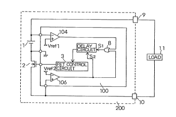
described with reference to the drawings. Fig. 1 is a block
CA 02234734 1998-04-14
--5--
diagram of the principal portions of a power supply unit
embodying the present invention. Note that, in Fig. 1 and in the
following descriptions, such components as are found also in the
prior art shown in Fig. 7 are identified with the same designa-
tions, and overlapping explanations will be omitted.
The FET control circuit 3 receives the output of the delay
circuit 101. When the delay circuit 101 does not yield an output
(i.e. when it outputs a low level), the FET control circuit 3
turns on the discharge control FET 2. When the delay circuit 101
outputs an OFF signal (i.e. when it outputs a high level), the
FET control circuit 3 turns off the discharge control FET 2.
The delay circuit 101 is designed to be switchable between
two delay times Tl and T2 (Tl > T2), and receives, as its first
input signal Sl, the output of the OR circuit 8 and, as its
second input signal S2, the output of the second power source
monitoring circuit 6. While the first input signal Sl is low,
the delay circuit 101 remains inactive and outputs a low level.
Accordingly, in normal condition, that is, as long as no overdis-
charge or overcurrent is detected by the first or second power
source monitoring circuit 4 or 6, the discharge FET 2 is kept on
to drive the external load 11.
When the first input signal Sl becomes high, the delay
circuit 101 raises its output to a high level at the end of the
delay time selected in accordance with the state of the second
input signal S2. Specifically, as long as no overcurrent is
detected, the second input signal S2 remains low, and the delay
time Tl is selected; by contrast, when overcurrent is detected,
the second input signal S2 becomes high, and the delay time T2 is
CA 02234734 1998-04-14
--6--
selected.
Accordingly, when either overdischarge or overcurrent is
detected, the discharge control FET 2 is turned off at the end of
the delay time T1 or T2, and thereby the overdischarge or
overcurrent is stopped. In addition; since the delay time- for
overdischarge detection is set longer than the delay time for
overcurrent detection, overdischarge and overcurrent can be
detected correctly.
Fig. 2 shows an example of the construction of the delay
circuit 101. In Fig. 2, numeral 21 represents a first input
terminal; numeral 22 represents a second input terminal; CC1,
CC2, CC3, and CC4 represent constant current sources that
respectively output currents Il, I2, I3, and I4 (I3 > I4); Q1,
Q2, and Q6 represent pnp-type transistors; Q3, Q4, and Q5
represent npn-type transistors; SW1, SW2, and SW3 represent
switching circuits; KSW represents a selecting circuit; Rl and R2
represent resistors; C represents a capacitor; and CV represents
a constant voltage source.
The transistors Q1 and Q2 form a differential pair, with
their emitters connected through the switching circuit SW2 to the
constant current source CC2. The base of the transistor Ql is
connected to the node a, which is connected, on the one hand,
through the switching circuit SWl to the constant current source
CCl and, on the other hand, to the capacitor C. The other end of
the capacitor C is connected to ground. The base of the
transistor Q2 is connected to the node b, which is connected, on
the one hand, through the switching circuit SW3 and the selecting
circuit KSW to two constant current circuits CC3 and CC4 and, on
CA 02234734 1998-04-14
the other hand, to the resistor Rl. The other end of the
resistor R1 is connected to ground. The collector of the
transistor Ql is connected to the collector and base of the
transistor Q3 that serves as the input transistor of a current
mirror circuit. The collector of the transistor Q2 is connected
to the collector of the transistor Q4 that serves as the output
transistor of the current mirror circuit. The emitters of the
transistors Q3 and Q4 are connected to ground. When the
switching circuit SW2 is turned on and thereby the emitters of
the transistors Q1 and Q2 are connected to the constant current
source CC2, these transistors Ql and Q2 are activated to operate
as a differential amplifier.
The base of the transistor Q5 is connected to the node c
between the collectors of the transistors Q2 and Q4. The
collector of the transistor Q5 is connected through the resistor
R2 to the constant voltage source CV. The emitter of the
transistor Q5 is connected to ground. The base of the transistor
Q6 is connected to the node d between the resistor R2 and the
collector of the transistor Q5, and the emitter of the transistor
Q6 is connected to the constant voltage source CV. The collector
of this transistor Q6 serves as the output terminal of the delay
circuit 101. The current flowing out of this collector is
converted into a voltage by a current-to-voltage conversion
circuit (not shown), and is then fed to the FET control circuit
3. It is also possible to drive the FET control circuit 3
directly with the output current without using the current-to-
voltage conversion circuit. The transistors Q5 and Q6 and the
resistor R2 constitute an output circuit that is connected to the
CA 02234734 1998-04-14
collector of the transistor Q2.
The delay circuit 101 receives its first and second input
signals Sl and Sz via the first and second input terminals 21 and
22 respectively. The first input signal S1 from the first input
terminal 21 is fed to the switching circuits SW1, SW2, and SW3,
and, when the first input signal S1 rises to a high level, the
switching circuits SWl, SW2, and SW3 are turned on. On the other
hand, the second input signal S2 from the second input terminal
22 is fed to the selecting circuit KSW, and this selecting
circuit KSW selects the constant current source CC3 when the
second input signal S2 is low and selects the constant current
source CC4 when the second input signal S2 is high.
Although, in the above embodiment, the overcurrent detection
signal from the second power source monitoring circuit 106 is
used as the second input signal S2, it is also possible to use
the overdischarge detection signal from the first power source
monitoring circuit 104 as the second input signal S2. In this
latter case, however, the selecting circuit KSW needs to select
the constant current source CC4 when the second input signal S2
is low and select the constant current source CC3 when the second
input signal S2 is high.
Having a construction as described above, the delay circuit
101 operates only when overdischarge or overcurrent is detected.
Specifically, in such a case, as soon as the base voltage of the
transistor Ql exceeds the base voltage of the transistor Q2, the
output current appears at the collector of the transistor Q6. At
this time, whereas the base voltage of the transistor Q2 rises
abruptly, the capacitor C causes the base voltage of the
CA 02234734 1998-04-14
_g _
transistor Q1 to rise gradually, and, in this way, a delay time
is created. This delay time can be varied by varying the base
voltage of the transistor Q2.
Now, let the resistance of the resistor Rl be R1. Then, the
base voltage of the transistor Q2 is I3 x R1 when overdischarge
is detected, and it is I4 x R1 when overcurrent is detected.
Since I3 > I4, the base voltage of the transistor Q2 is higher
when overdischarge is detected than when overcurrent is detected,
and accordingly the delay time for overdischarge detection is
longer than the delay time for overcurrent detection. Fig. 4
shows the difference between the delay times for overdischarge
detection and overcurrent detection. In Fig. 4, to indicates the
time point when overdischarge or overcurrent is detected, T2
represents the delay time that is created when overcurrent is
detected, and T1 represents the delay time that is created when
overdischarge is detected.
Even if the capacitance of the capacitor C varies from unit
to unit, the delay times for overdischarge and overcurrent vary
in the same direction. Accordingly, the relationship between the
two delay times never happens to be reversed, and thus it is
possible to detect overdischarge and overcurrent correctly.
For example, in the embodiment under discussion, in which
one lithium-ion cell (voltage ~ 3.6 V per cell) is connected,
I4 x R1 is set to 2.3 V and I3 x R1 is set to 3 5 V, so that Tl
is longer than T2 by approximately 10 ms.
The present invention is applicable not only to an embodi-
ment as described above, but also to a lithium-ion cell power
supply unit in which a charge control FET is inserted between the
CA 02234734 1998-04-14
--10--
discharge control FET 2 and the output terminal 10.
Moreover, in the delay circuit 101, the constant current
sources CC3 and CC4, shown in Fig. 2, for generating the base
voltage of the transistor Q2 may be connected as shown in Fig. 3.
In that case, the selecting switch KSW is so configured that it
is turned off when the second input is high and it is turned on
when the second input is low.
The above described power supply unit requires only one
delay circuit, and therefore it can be realized with less cost
and with a smallçr IC chip area. In addition, since a single
delay circuit is used to create the delay times for both
overdischarge detection and overcurrent detection, even if the
delay times vary from unit to unit, the relationship between the
two delay times never happens to be reversed, and therefore it is
possible to detect overdischarge and overcurrent correctly.
Next, an example of the construction of the power source
monitoring circuits 104 and 106 shown in Fig. 1 will be described
with reference to Fig. 5. The power source monitoring circuit
104 is for overdischarge detection, and the power source
monitoring circuit 106 is for overcurrent detection. These power
source monitoring circuits 104 and 106 are realized with a
construction similar to that of the delay circuit shown in Fig.
2. Accordingly, in Fig. 5, which shows an example of the
construction of the power source monitoring circuit, and in the
following descriptions, such components as are found also in Fig.
2 are identified with the same designations, and overlapping
explanations will be omitted. Note also that the following
descriptions deal with the case where the circuit shown in Fig.
CA 02234734 1998-04-14
5 is applied to the power source monitoring circuit 106 for
overcurrent detection.
The power source monitoring circuit receives, at the input
terminal 21, a signal SA, which is, for example, a high-level
signal that is generated when the power supply unit 200 returns
from an overcurrent or overdischarge state to a stand-by state
(the stand-by state refers to a state in which the power supply
unit 200 is ready for overcurrent or overdischarge detection).
On the other hand, the power~source monitoring circuit also
receives, at another input terminal 31, a signal SB, which is a
voltage that appears across the ON resistance of the F~T 2.
The input terminal 21 is connected to the switch SW1 through
a delay circuit D. Accordingly, when the input signal SA is
received, whereas the switches SW2 and SW3 are turned on immedi-
ately, the switch SWl is turned on with a delay. If this delaycircuit D is not provided, the switches SW1, SW2, and SW3 are,
theoretically, turned on at the same time. In reality, however,
variations of the characteris~ics of the circuit elements or
other factors may cause the base voltage of the transistor Q1 to
rise earlier than the base voltage of the transistor Q2, with the
result that the transistor Q6 outputs a current that indicates
detection of overcurrent. That is, in such a case, even though
the input signal SB is not receiVed at the input terminal 31, the
overcurrent detection current is outputted erroneously. By
contrast, if the delay circuit D is provided as shown in the
figure, it causes the base voltage of the transistor Q1 to rise
later than the base voltage of the transistor Q2, and thus it
prevents erroneous current output that may occur when the power
CA 02234734 1998-04-14
-12-
supply unit returns to the stand-by state.
It is possible to omit the delay circuit D by omitting the
switehes SW1 and SW3 and instead connecting the constant current
sourees CC1 and CC3 directly to the bases of the transistors Q1
and Q2 and by eontrolling only the switeh SW2 with the input
signal SA. However, in that case, the eonstant eurrent sourees
CC1 and CC3 need to supply eurrents I1 and I3 of a few miero-
amperes eonstantly. Quite disadvantageously, this not only
inereases eurrent eonsumption, but also aggravates overdiseharge
of the battery paek and thus deteriorates its eharaeteristies.
When the switeh SW1, subsequent to the switches SW2 and SW3,
is turned on, the power supply unit enters the stand-by state.
In this state, while the signal SB is low enough, the transistor
Q6 does not output the overcurrent deteetion eurrent from its
eolleetor, but, when the signal SB exeeeds a predetermined value,
the transistor Q6 is turned on and outputs the overeurrent
detection current. This overcurrent detection current is fed to
the delay circuit 101 described previously (Fig. 2). Note that,
although the above description deals with the case where the
circuit shown in Fig. 5 is applied to the power source monitoring
cireuit 106 for overeurrent deteetion, the eireuit shown in Fig.
5 is applieable also to the power souree monitoring eircuit 104
for overdiseharge detection.
Fig. 6 shows another example of the eonstruction of the
power souree monitoring eireuit shown in Fig. 5. In Fig 6, CC
represents a eurrent souree that outputs a eurrent I, Q7 to Q10
are pnp-type transistors whose bases are eonneeted together and
whose emitters are eonneeted to a direet-current voltage source
CA 02234734 1998-04-14
-13-
CV, and C represents a capacitor for realizing a delay; in
addition, such components as are found also in Fig. 5 are
identified with the same designations.
In Fig. 6, the transistors Q8, Q9, and Q10 each form a
current mirror circuit together with the transistor Q7. In these
current mirror circuits, the transistor Q7 serves as the input
transistor, and the transistors Q8, Q9, and Q10 each serve as the
output transistor. The collector of the transistor Q8 is
connected to one end of the capacitor C, and, to this node
between the collector of the transistor Q8 and the capacitor C,
the base of the transistor Ql is connected. The other end of the
capacitor C is connected to ground. The collector of the
transistor Q10 is connected to a resistor R1, and, to this node
between the collector of the transistor Q10 and the resistor R1,
the base of the transistor Q2 is connected. Further, the
emitters of the transistors Ql and Q2 are connected to the
collector of the transistor Qg.
When fed with a control signal that indicates detection of
overcurrent or overdischarge, the constant current source CC is
turned on and extracts a current I from the input transistor of
the above-mentioned current mirror circuits. As a result, the
current I starts flowing through the capacitor C and through the
resistor R1 at the same time, causing the base voltages of the
transistors Ql and Q2 to rise. Here, if the capacitance of the
capacitor C is assumed to be C, then the base voltage of the
transistor Q1 rises with a slope I/C.
Accordingly, as long as the capacitance of the capacitor C
is determined appropriately, the relationship between the rising
CA 02234734 1998-04-14
-14-
times of the base voltages of the transistors Q1 and Q2 can be
kept as initially set without the need to supply currents
beforehand, and thus erroneous operation of the power source
monitoring circuit can be prevented.
The base voltage of the transistor Q1 keeps rising as time
passes, and the time it takes to exceed the base voltage of the
transistor Q2 is the delay time obtained by the power source
monitoring circuit.
In Figs. 5 and 6, instead of feeding external signals to the
power source monitoring circuit, it is also possible to vary the
current outputted from the constant current course CC1 in such a
way that the relationship between the base voltages of the
transistors Q1 and QZ is reversed at the end of a predetermined
length of time.
In the above described power monitoring circuit, an initial
state is established not by supplying currents beforehand, but by
lengthening the rising time of a base voltage. As a result, this
power monitoring circuit never operates erroneously, and in
addition reduces the current consumption in an overdischarge
state to approximately as low as a leak current (below 1 ,uA).
Thus, it is possible to prevent deterioration of the characteris-
tics of a battery pack.
Industrial applicability
As described above, according to the present invention, a
power supply unit requires only one delay circuit, and therefore
it can be realized with less cost and with a smaller IC chip
area. In addition, since a single delay circuit is used to
-
CA 02234734 1998-04-14
-15-
create the delay times for both overdischarge detection and
overcurrent detection, even if the delay times vary from unit to
unit, the relationship between the two delay times never happens
to be reversed, and therefore it is possible to detect
overdischarge and overcurrent correctly. Accordingly, the
present invention is useful in a power supply unit that uses
secondary batteries as a power source, in particular in such a
power supply unit in which signals indicating detection of
overdischarge and overcurrent need to be outputted with different
delays, for example a power supply unit having a power source
consisting of batteries, an overdischarge detection circuit for
detecting overdischarge of the power source, and an overcurrent
detection circuit for detecting overcurrent.
~ . . . . . . . . .