Note: Descriptions are shown in the official language in which they were submitted.
CA 02234780 2004-09-02
-1-
TAPERED WAVEGUIDE FOR OPTICAL DISPERSION COMPENSATION
Field of the Invention
The present invention relates to a waveguide for providing optical dispersion
management of a single channel or multiple channels in a wavelength division
multiplexing (WDM) optical communication system. In particular, the invention
provides
an optical waveguide which creates large positive or negative dispersion so as
to
compensate for dispersion of pulsed light transmissions passing through
optical fiber
systems.
Background of the Invention
One of the fundamental problems which exist in long haul high rate optical
communications is chromatic dispersion of light pulses passing through fiber
optic lines.
This dispersion causes different wavelengths to travel through the optical
waveguide at
different speeds. An optical communications light pulse which is part of a bit
stream is
created by a transmission laser operating at a predetermined carrier optical
frequency or
wavelength (the words frequency, represented by f, and wavelength in vacuum,
represented by ~,, will be used interchangeably, as is currently done in the
art, with ~,
related to f by the equation ~, = c/f, where c is the speed of light, viz. 299
792 458 m/s).
The pulse has a given intensity and duration which can be detected at a
receiver
located at an opposite end of the communications waveguide (typically the
optic fiber)
some distance away from the transmitter, perhaps a few to tens of kilometers
away. The
light pulse comprises spectral components covering a certain bandwidth Df,
which is
generally in the range 10-60 GHz in modern optical communications systems
operating in
the bit rate range of 2.5-10 Gb/s. In optical fibers used for communications,
the group
velocity associated with each spectral component varies with its optical
frequency (or
wavelength). This means that the low frequency spectral components of a light
pulse do
not travel at the same velocity as its high frequency components. This causes
a light pulse
initially injected into a fiber with duration Dt to broaden out (in others
words to become
"dispersed") to a duration Df after propagating through a certain length of
optical fiber.
As an example, in conventional fibers deployed over land, the dispersion is
typically 17
CA 02234780 2004-09-02
-2-
ps/nm/km. This means that two spectral components separated by say 10 GHz at a
Garner
frequency of 193 000 GHz (~. = 1553.329 nm), corresponding therefore to a
wavelength
separation of 0.0804 nm, would undergo a differential delay (or dispersion) of
17
ps/nm/km times 0.0804 nm, i.e. 1.37 ps/km, or 137 ps after 100 km of fiber
(the sign of
the dispersion in conventional fibers is such that low frequency light travels
at a lower
group velocity than high frequency light). Light pulses that may be initially
25 ps in
duration in a 10 Gb/s optical communication system have spectral components
that cover
several tens of GHz. The time dispersion between the low- and the high-
frequency
spectral components of such a light pulse are therefore more than 137 ~ps
after a 100-km
stretch of fiber. Such a large amount of dispersion is intolerable since, the
pulses being
100 ps apart, dispersion will make subsequent pulses start overlapping to a
considerable
degree and increase the bit error rate.
Therefore, dispersion causes a spreading of laser pulses over great distances
(even
in the most non-dispersive optic fibers) such that the pulse energy is spread
out and lower
frequency spectral components trail behind higher-frequency components of the
laser
pulse.
When the bit time slot in an optical communication system is large enough,
dispersion causes a small portion of the pulse energy to spill over into
adjacent bit time
slots. The pulse height at the receiver will be marginally lower, but still
detectable as a
bit, and empty bit slots (e.g. representing zeros) will contain small amounts
of spill over
light, which will be below the predetermined detection threshold. However, as
the bit
time slots are made smaller so as to increase the bit rate and increase
transmission
capacity, dispersion of a very short light pulse may significantly reduce the
light intensity
in the bit time slot and even cause enough spill over into adjacent empty bit
time slots so
as to cause difficulty in the detection of zeroes.
Dispersion thus produces the spreading of short optical pulses, and thus
affects
negatively the quality of a communication link. If the dispersion of a light
pulse is great
enough, the communication link utilizing the light pulses becomes unstable,
and
eventually, unusable.
In addition to problems in optical communications, dispersion is also a major
problem in the generation of very short, high power optical laser pulses. The
spreading of
CA 02234780 2004-09-02
-3-
the pulses reduces the achieved peak power, and thus reduces the efficiency of
the laser
pulses.
Various attempts have been made to address the problem of dispersion in
optical
signals. Three basic approaches have been developed. The first approach is to
pass the
optical signal transmitted, which has suffered dispersion due to the optical
transmission
waveguide, through a length of waveguide having an opposite sign of dispersion
at the
communications wavelength before feeding the signal to the receiver. U.S.
Patent
4,969,710 to Tick et al. is an example of such a method. The second approach
has been to
use optical devices to separate the light pulse into its wavelength
components, then to
subject the separated components to different delays before recombining the
components
into a single dispersion compensated optic signal. U.S. Patent 5,473,719 to
Stone is an
example of this approach. The third approach has been to use chirped in-fiber
Bragg
gratings to reflect each wavelength component at different points such that
the reflected
optical signal has been dispersion compensated. This approach is disclosed in
a paper by
1 S Fran~ois Ouellette, titled "Dispersion cancellation using linearly chirped
Bragg grating
filters in optical waveguides", Optics Letters, vol. 12, pp. 847-849, October
1987.
Experimental results have been reported in the paper by W.H. Loh, R.I. Laming,
N.
Robinson, A. Cavaciuti, F. Vaninetti, C.J. Anderson, M.N. Zervas, and M.J.
Cole, titled
"Dispersion compensation over distances in excess of 500 km for 10-Gb/s
systems using
chirped fiber gratings", IEEE Photonics Technology Letters, vol. 8, pp. 944-
946, July
1996.
Other known prior art attempts to resolve these problems are disclosed in U.S.
Patent 5,570,439 to Ido et al.; U.S. Patent 5,568,583 to Akasaka et al; U.S.
Patent
5,559,920 to Chraplyvy et al.; U.S. Patent 5,530,778 to Rast; U.S. Patent
5,504,829 to
Evans et al.; U.S. Patent 5,448,674 to Vengsarkar et al.
Known dispersion compensators are bulky, generally limited to a single channel
wavelength and/or have significant losses. The advantage of the dispersion
management
device proposed here is that it could be manufactured using integrated optic
techniques so
that it could be very compact and low-cost. In addition the taper lends itself
very naturally
to tailoring the dispersion as a function of wavelength in a way to match (and
compensate) that of an optical fiber. In 10 Gb/s and higher bit rate system
the variation of
< CA 02234780 2004-09-02
-4-
the dispersion with wavelength (from 16 ps/nm/km at 1530 nm to 17 ps/nmllon at
1580
nm, for example, in certain optical fibers) is a factor that is now
considered. Our device
can offer this wavelength tailored dispersion profile and can do so over very
broad
wavelength bands.
S
Summary of the Invention
It is an object of the present invention to provide a dispersion compensator
which
makes use of a wavelength dependent transition between two optical waveguide
media
having different indices of refraction to carry out dispersion compensation It
is a further
object of the present invention to provide a compact, low loss optical
waveguide device
for carrying out dispersion compensation.
Therefore, it is an object of the present invention to provide a dispersion
compensator in which the light pulse must travel from a first medium having a
first
typically low refractive index to a second medium having a second typically
high
refractive index, and back to the first medium so as to introduce a
differential delay
between the low- and high-frequency spectral components of a light pulse.
It is another object of the present invention to provide a dispersion
compensator
which can be used for compensating dispersion of certain light frequency bands
by
altering geometrical or material characteristics of the dispersion
compensator.
These and other objects are achieved by a dispersion compensator formed by
joining together two discrete layers of material having two different indexes
of refraction
into a single unit. The first layer of material is substantially planar and of
substantially
uniform thickness and the second layer of material is tapered on its upper
surface. The
taper is such that during the first half of a pulse's passage through the
compensator the
high-index material tapers up, while in the second half it tapers down. The
layers of
material are designed to have a large absolute difference index (fin greater
than 0.5), so
that when an optical pulse passes from the first layer of material to the
second layer of
material, a differential delay is introduced between the low- and high-
frequency
components of the pulse due to the difference in the refractive index.
When the optical pulse emerges from the second bottom layer of material and
returns to the first top layer of material, the differential delay introduced
is such that the
CA 02234780 2004-09-02
-5-
waveform dispersion is compensated for the dispersion caused by the spreading
of the
pulse during its travel through a fiber optic link. The result is an optical
pulse in which the
dispersion is negated, and the pulse thus becomes usable in its desired
application. In
another feature of the present invention, the geometry and material
characteristics of the
dispersion compensator can be specifically designed so as to produce positive
or negative
dispersion, or to alter the degree of dispersion, depending upon the desired
application.
According to the invention, there is provided an optical device comprising: an
input; a first waveguide having a first low index of refraction and a lateral
coupling
surface, the first waveguide able to guide a mode of light; a second waveguide
having a
second high index of refraction significantly different from the first index
of refraction, a
corresponding lateral coupling surface coupled to the lateral surface of the
first
waveguide, the second waveguide having a variable thickness selected to allow
a
predetermined wavelength to pass between the first and the second waveguide at
a
predetermined distance from the entrance face of the device; and an output.
Preferably, the input is at one end face of the first waveguide, and the
output
comprises a first output at another end face of the first waveguide.
Also preferably, the thickness varies gradually so as to allow neighboring
wavelength components of an optical signal to undergo chromatic dispersion by
coupling
from the first waveguide to the second waveguide at different positions.
According to the invention, there is provided an optical device for creating
chromatic dispersion which comprises an input receiving an optic
communications signal,
a first waveguide, a second waveguide and an output for outputting the optic
communications signal with . modified chromatic dispersion characteristics.
The first
waveguide has a first index of refraction and a lateral coupling surface and
is able to guide
a mode of light. It has a substantially uniform thickness. The second
waveguide has a
second index of refraction significantly different from the first index of
refi~action and a
corresponding lateral coupling surface coupled to the lateral surface of the
first
waveguide. It also has a variable thickness selected to allow a predetermined
wavelength
to couple massively from the first to the second waveguide at a predetermined
distance
along the coupling surface in the direction of propagation of the mode of
light, the
thickness varying gradually in the direction of propagation of light so as to
allow
~
CA 02234780 2004-09-02
-6-
neighboring wavelength components of an optical signal to undergo chromatic
dispersion
by coupling from the first waveguide to the second waveguide at different
positions.
Brief Description of the Drawings
The invention will be better understood by way of the following detailed
description of a preferred embodiment and alternate embodiments with reference
to the
appended drawings, in which:
Fig. 1 is a schematic diagram of a photonic communications link including a
chromatic dispersion compensator;
Fig. 2 is a cross sectional view of a preferred embodiment for a high
performance
tapered waveguide for a broad-band WDM optical dispersion compensator
according to
the present invention;
Fig. 3 illustrates in block format the preferred embodiment including input
and
output mode converters;
Fig. 4 illustrates a device for dispersion management where long wavelength
components travel faster than short wavelength components, having. a high
index layer
that first tapers down and then up;
Fig. 5 illustrates a device with a programmed taper profile such that optical
signals in channel 1 will undergo a certain dispersion that is less than the
dispersion
compensation undergone by optical signals in channel 2, because of the
differing slopes of
the taper; and
Fig. 6 illustrates a parabolic profile to obtain a dispersion which is
linearly
increasing with wavelength within a communications band.
Detailed Description of the Preferred Embodiments
As shown in Fig. 1, an optical communication link comprises a sending or
transmitting light source, such as a diode laser 12, generating a pulse train
13 optically
coupled to a fiber 14. Over a great distance, the square pulse train 13
undergoes
chromatic dispersion causing the pulses to appear at the remote end with
spreading as
shown at 15. The compensator 1 restores the pulses before detection at a
detector 16.
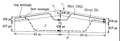
In the preferred embodiment, as illustrated in Figs. 2 and 3, the dispersion
CA 02234780 2004-09-02
-7_
compensator device 1 comprises three components, namely an input mode
converter la, a
dispersive waveguide lb, and an output mode converter lc. The structure of the
dispersive waveguide lb is as shown in Fig. 2a. A first waveguide 2 is made of
silica
(Si02) and has a thickness of 10.00~m. A second waveguide 3 is made of silicon
(Si)
and has a tapered thickness starting at 42.37~m and having a thickness in the
middle of
42.60~m. The thickness variation is exaggerated in the drawing for the
purposes of
illustration. In the first half of the device where the high-index silicon
layer is tapering
up, the longer wavelengths couple and pass from the silica to the silicon at a
propagation
distance further from the input than the shorter wavelengths. In the second
half of the
device where the high-index silicon layer is tapering down, the reverse
occurs, and the
longer wavelengths are the first to couple back from the silicon into the
silica. Thus the
shorter wavelength components go through much more silicon than the longer
wavelength
components. Since the index of refraction of the silica is about 1.44, while
for the silicon
it is about 3.48, the shorter wavelengths which spend more time in the silicon
are slowed
down more with respect to the longer wavelengths. The effect is to cause
compensation
of the chromatic dispersion caused by the fiber 14 which slows down redder
components
more than bluer components. The component lb has a length of about 20 cm.
The device is so designed that the distance at which light at a given optical
frequency will couple from the low-index silica layer into the high-index
silicon layer is
determined by the programmed taper in the high-index layer. Transfer of the
optical
power from the low-index layer to the high-index layer occurs near a resonance
in the
latter, i.e. when the lateral mode profile of the optical electric field
comprises an integral
number of half wavelengths (the transverse wavelength in the medium is what is
meant
here) within the thickness of high-index material at that point on the taper.
As a light
pulse travels down the up-taper its high-frequency spectral components (which
are the
short-wavelength spectral components) are the first to enter into resonance
with the high-
index layer, and are therefore the first to couple massively into this high-
index layer.
Some distance further down the lower-frequency components (longer-wavelength
components) enter into resonance and in turn couple massively into the high-
index layer.
The group velocity of light in the high-index layer is much slower (it is
typically
0.13c in the example given with silicon) than in the low-index layer (it is
typically 0.6c in
CA 02234780 2004-09-02
_$_
the example given with silica). The longer a given spectral component travels
in the high-
index layer, therefore, the more it is delayed relative to a spectral
component that is
traveling in the low-index layer.
To obtain a high dispersion, it is best to excite only one specific mode of
the
waveguide 2. The mode converters 1 a and 1 c thus increase efficiency. The
mode
converters may comprise holograms, adiabatic taper waveguides, phase masks or
amplitude masks. The mode converter devices according to the preferred
embodiment
also guide the light from the first waveguide 2 to the input and output
fibers.
The waveguide lb is formed from a first waveguide layer of material 2 having a
generally uniform thickness, and a second layer of material 3 that has a
generally non
uniform thickness which defines a tapered upper surface (likewise the tapered
surface
may be the lower surface). The first layer of material and second layer of
material are
intended to have substantially different refractive indexes, such that the
absolute
difference in refractive index is preferably greater than 0.5. Preferred
materials which
achieve this absolute difference are silca and silicon for the wavelength
range 1200 to
1800 nm where both materials are very transparent, although other optically
transparent
materials which obtain this same magnitude of difference in refractive index
are also
considered to be within the scope of the present invention. The thickness of
the first layer
of material (D1) and the thickness of the second layer of material (D2) should
also be
relatively large in comparison to the wavelengths of light passing through the
respective
mediums. For applications in optical communications, D 1 should preferably be
greater
than or equal to 2 micrometers, and D2 should preferably be greater than or
equal to 10
microns. Other dimensions for D1 and D2 may be utilized within the scope of
the present
invention.
As shown in Figs. 4 through 6, the thickness profile of the second waveguide 3
may take on a variety of shapes. In Fig. 3 the simple linear taper gives a
dispersion
compensation which is constant over a band of about 7 nm (or 870 GHz in
optical
frequency). This would be enough bandwidth to compensate the dispersion of
eight
optical channels spaced by the standard 100-GHz channel spacing. Larger
bandwidths can
be achieved by using thinner layers of silicon. The constant dispersion
bandwidth then
increases in inverse proportion to the silicon thickness, but its magnitude
decreases in
CA 02234780 2004-09-02
-9-
direct proportion to the silicon thickness. For a given device a greater
dispersion effect
can be obtained by making several passes though the device.
In Fig. 4, the device has a high-index layer which first tapers down and then
up.
The reverse of what was happening in Fig. 3 now occurs. The long wavelength
("redder")
spectral components of a light pulse will be the first to couple massively
into the high
index layer (i.e, silicon, in one preferred embodiment) and they will be the
last to exit the
high-index layer and couple back into the low-index layer. The shorter
wavelength
("bluer") components will couple further down the initial down-taper than the
long
wavelength components and they will be the first to couple back into the low-
index layer.
The long wavelength components spend therefore more time in the silicon than
the shorter
wavelength components.
The device of Figs. 2a and 3 operates as follows. Light pulses from an optical
communications transmission are injected into the silica layer 2 at the left.
As light
begins to propagate its power distribution is largely confined to the silica
layer. This is
assured by having a silicon thickness near the input end face such that the
silicon layer
behaves as an anti-resonant reflector as in the well-known ARROW (anti-
resonant
reflecting optical waveguide) devices. As explained earlier, the light pulse
comprises a
spread of spectral components in the immediate vicinity of the carrier
frequency. As the
light pulse travels down the structure, there will first come a point along
the taper where
high frequency components begin to couple massively into the high-index layer
because
of a resonance condition (at this point the silicon ceases to be an anti-
resonant reflector to
become a resonant one; the light electric field builds up resonantly in the
silicon). Further
down the taper, low frequency spectral components will in turn couple
massively into the
high-index silicon layer.
As the light pulse continues to sweep down the path of the compensator, the
silicon layer reverses from an up-taper to a down-taper. The reverse process
now occurs.
At a point symmetric to the one where resonant coupling took place for a given
spectral
component, now optical power at that frequency couples back massively into the
silica
layer.
Because the silicon layer has a different index of refraction than the silica
layer,
and the high frequency components are confined to the silicon layer for a
greater portion
CA 02234780 2004-09-02
-10-
of the sweep through the compensator, the high frequency components of the
pulse are
slowed down relative to the low frequency components. This causes the waveform
of the
optical pulse to become much more uniform, and provides a substantial
compensation for
waveforms that have dispersed during travel though an optical fiber.
In the case of Figs. 2, 3, 5 and 6, the dispersion that is created by the
taper device
is "normal", i.e. it compensates for the anomalous dispersion (in anomalous
dispersion
redder spectral components travel slower than bluer components, the reverse is
true for
normal dispersion) of optical fibers in the 1500 nm band. In dispersion
management one
sometimes wishes to have an element with an anomalous dispersion. The device
shown in
Fig. 4 accomplishes that. The mode of operation is exactly as in the up-
taper/down-taper
device except that the roles of the bluer and redder spectral components are
reversed.
Fig 5. shows an example of how the silicon layer thickness can be programmed
to
give a dispersion that is wavelength dependent. Assume a spectrum divided into
a short
wavelength band called BAND 1 and a long wavelength band called "BAND 2". For
the
part labeled "BAND 1" the slope might be such that it would compensate a fiber
dispersion of say 16 ps/nm/km. Those optical signals falling within this band
will come
into resonance with the silicon in this first region of the taper and will
experience a
dispersion that would compensate this 16 ps/nm/km in a certain length of
fiber. A second
group of optical signals falling within the spectral band 2 will come into
resonance with
the silicon in the part of lower slope labeled "BAND 2". The magnitude of
dispersion is
inversely proportional to the slope of the taper. So, for band 2 the slope
might compensate
for say a fiber dispersion of 17 ps/nmJkm. These dispersion figures apply to
current
conventional optical communications fibers for the short and long wavelength
half of the
Erbium band between 1530 and 1560 nm. In other cases, especially when a fiber
is
operated near a dispersion minimum, thevariation of dispersion with wavelength
could be
more severe, so that the tailored dispersion offered by the device of Fig. 5
would be all the
more useful.
For certain applications it might be useful to have several sections of the
taper
with different slopes. In this spirit , Fig. 6 shows a taper displaying a
parabolic profile,
such that the slope is increasing linearly with propagation distance. This
will produce a
dispersion which is progressively larger as the wavelength increases. This
would be a
CA 02234780 2004-09-02
-11-
good match for the dispersion in fibers which increases progressively with
wavelength as
one moves away from a dispersion minimum.
In view of these characteristics, it can be seen that the compensating device
of the
present invention can be specifically designed to produce a desired dispersion
for a
specific application. High degrees of difference between the indexes of
refraction for the
two layers of material produce a greater degree of dispersion in the high
frequency
components of the optical pulse. The shape of the upper surface of the
compensator
influences whether the dispersion is negative or positive. The thickness of
the lower layer
and the slope of this layer influence where the compensator converts from an
anti-
resonant reflector to a resonant reflector. By adjusting any one of these
different variables
in the manufacture of the compensator device, the compensator can be adjusted
for
different types of applications, depending on the types of dispersion problems
which are
encountered by a user.
As can be appreciated, it would be possible to place a reflector at a middle
point of
the device lb to provide for dispersion compensation in a reflective device,
much like a
chirped Bragg grating device. This is shown in Fig. 2 b. Of course, this
device must be
used in conjunction with an optical circulator.